1. Introduction
Diagnostic imaging in nuclear medicine is a functional technique widely used in many procedures and clinical investigations. Specific examinations are done in terms of imaging or tomography. Typically, most diagnostic images are acquired using either a SPECT or a PET scanner [
1,
2,
3], which in recent years have been pushed towards co-registration modalities like SPECT-CT and PET-CT [
4]. These are based on gamma rays or positrons emitted by the human body and then imaged with very large instruments, surrounding the body, using the same premise as a CT scanner to create a 3D reconstruction from a series of gamma detections acquired at different imaging angles. For SPECT and PET, the detected photons are gamma rays generated inside the patient after administration of a radiopharmaceutical. The 3D representation provided by SPECT or PET imaging [
5] is regularly used for preoperative surgical planning. However, such imaging systems are too large and cannot be used during surgery.
On the contrary, in radio-guided surgery (RGS), typically non-imaging gamma probes are used [
6,
7]. These are handheld, light, and easy to use. The surgeons rely on the probe’s detected count rate (e.g., indicated by an audible signal) to identify regions of high uptake for excision or further investigation.
The possibility of combining the advantages of the two previously mentioned techniques, i.e., small, compact devices but with imaging capabilities, would be highly beneficial for the surgeons and for better lesion identification in the surgery room. Indeed, recently, small portable gamma cameras started to be developed for different applications, including medical imaging, like in RGS [
7,
8,
9,
10,
11], sentinel node detection [
12,
13,
14], and sentinel lymph node biopsy (SLNB), for example for breast cancer [
8,
15], sometimes performed at the same time with sentinel node and occult lesion localization (SNOLL) [
15,
16]. Such compact gamma cameras (CGCs), also referred to as intraoperative gamma cameras (IGCs) [
7,
17], portable gamma cameras [
14,
18,
19], handheld gamma cameras [
8], or Tumor Resection Cameras [
15], can be used before and during surgery, giving information regarding the location and extension of malignant disease [
8,
15,
17], thus allowing surgeons to minimize surgical invasiveness [
11,
13,
15]. However, this is only possible if their sensitivity, ease of use, and other practical aspects are as good as the current probes. Moreover, being an imaging device, they should also have good energy resolution and spatial resolution.
Some authors reported examples of compact gamma cameras for medical imaging applications, particularly for radio-guided surgery. Some of them are mounted on articulated arms, easily movable, and attached to the stage with the PC [
11,
14,
15]. They might have laser pointers to highlight the area under investigation, showing on the screen the image of the emission from the investigated region of the patient’s body [
14]. A step forward in the direction of a better ease-of-use is to make these cameras smaller, lighter, and handheld. Such a system might be still cable connected to a PC station for power and data connections [
8,
13,
18,
19], or it might be completely wireless [
9,
10,
20]. Some of them are based on a compact design and may include a small onboard monitor to visualize the emission from the investigated region [
9,
10], whereas others are based on a hybrid system with a co-registration of gamma-ray and optical images, thus combining the two images on the PC [
18,
19].
In this paper, we present a compact, low-power, wireless, handheld gamma camera developed for radio-guided surgery. This has been developed within the ATTRACT POSICS-2 project [
21] (“POSICS2 camera”). The photosensor is made up of large-area Silicon Photomultipliers (SiPMs) [
22,
23]. We used a particular position-sensitive Silicon Photomultiplier technology, namely the FBK linearly graded SiPM (LG-SiPM) technology [
24,
25]. The detector is made up of a 3 × 3 array of 10 × 10 mm
2 SiPM chips (connected and used as described in [
26]), having an area of about 31 × 31 mm
2. Thanks to this detector technology, it is possible to significantly reduce the number of readout channels to just eight [
27]; thus, the number of amplification stages in the front-end electronics and the number of simultaneously sampled channels in the analog-to-digital conversion stage. This, in turn, simplifies the complexity and lowers the power consumption of all the readout electronics, allowing for a light, battery-powered, compact gamma camera.
Compared with other implementations, we focused on having a completely stand-alone system—hence, the wireless communication and recharge and battery-powered design. The detection area and the field-of-view (FoV), as well as the energy and spatial resolution, are comparable with other state-of-the-art implementations [
7,
11]. In the paper, we detail the detector technology used, the design of the camera, the electrical simulations, and the measured performance.
2. Silicon Photomultiplier Detector
Silicon Photomultipliers (SiPMs) are single-photon-sensitive detectors that continue to attract increasing interest in several industrial and scientific applications that require fast detection, high sensitivity, compactness, insensitivity to magnetic fields, and low bias voltages [
22,
23]. Analog SiPMs are made up of a hundreds or thousands of single-photon avalanche diodes (SPADs) (“microcells”) connected in parallel, each one with its own quenching resistor in series, thus providing at the output a pulse with an amplitude (and charge) that is proportional to the number of detected photons [
22]. They are used in applications like Positron Emission Tomography in conjunction with time-of-flight information (ToF-PET) [
28,
29], the Cherenkov light readout [
30,
31], Light Detection and Ranging (LiDAR) systems [
32], and others. In FBK (Trento, Italy), we developed different technologies for SPADs and SiPMs in recent years that are customized and optimized for different applications [
33], for example, NUV-HD technology (where sensitivity peaks in the near-ultraviolet range) and RGB-HD technology (where sensitivity peaks at the green wavelength).
Position-Sensitive SiPMs
In many applications, there is the need to have high-sensitivity photodetectors that cover large active areas but preserve the particle (or photon) arrival position information. This can be done for example with arrays of SiPMs, having tens of elements, each one read out by a dedicated front end. These SiPM arrays are employed in applications like MR-compatible PET or in space applications; however, in some cases, the system complexity or simply the number of readout channels need to be reduced as much as possible [
34]. In these cases, an alternative solution is using position-sensitive SiPMs (PS-SiPMs), especially with large-area chips (or arrays of large chips).
In PS-SiPM, each chip has four readout channels (providing top, bottom, left, and right coordinates) instead of just one. Different technological solutions have been developed, e.g., “Sensitivity-encoding” SiPMs (SeSP) [
35] and “interpolating” SiPMs [
36], a 2D resistive network [
37], a continuous resistive layer on top of all microcells combined with an epi-layer resistor [
38], etc. In FBK, we developed the linearly graded (LG-SiPM) technology [
24,
25,
26,
27], which is based on an avalanche–current weighted–partitioning approach. Each microcell is connected to two quenching resistors (not just one); one is used for the vertical current divider and the other for the horizontal current divider. In the current dividers, the current is split between the two outputs, i.e., top/bottom (or left/right) in a way that the amplitude (and total charge) changes linearly with the vertical (or horizontal) position [
25].
In the reported gamma camera, we used a 3 × 3 array of 10 × 10 mm
2 LG-SiPM chips, based on NUV-HD technology (see
Figure 1), with peak sensitivity at 420 nm, a breakdown voltage of ~32 V, and a microcell pitch of 25 µm. Moreover, as reported in [
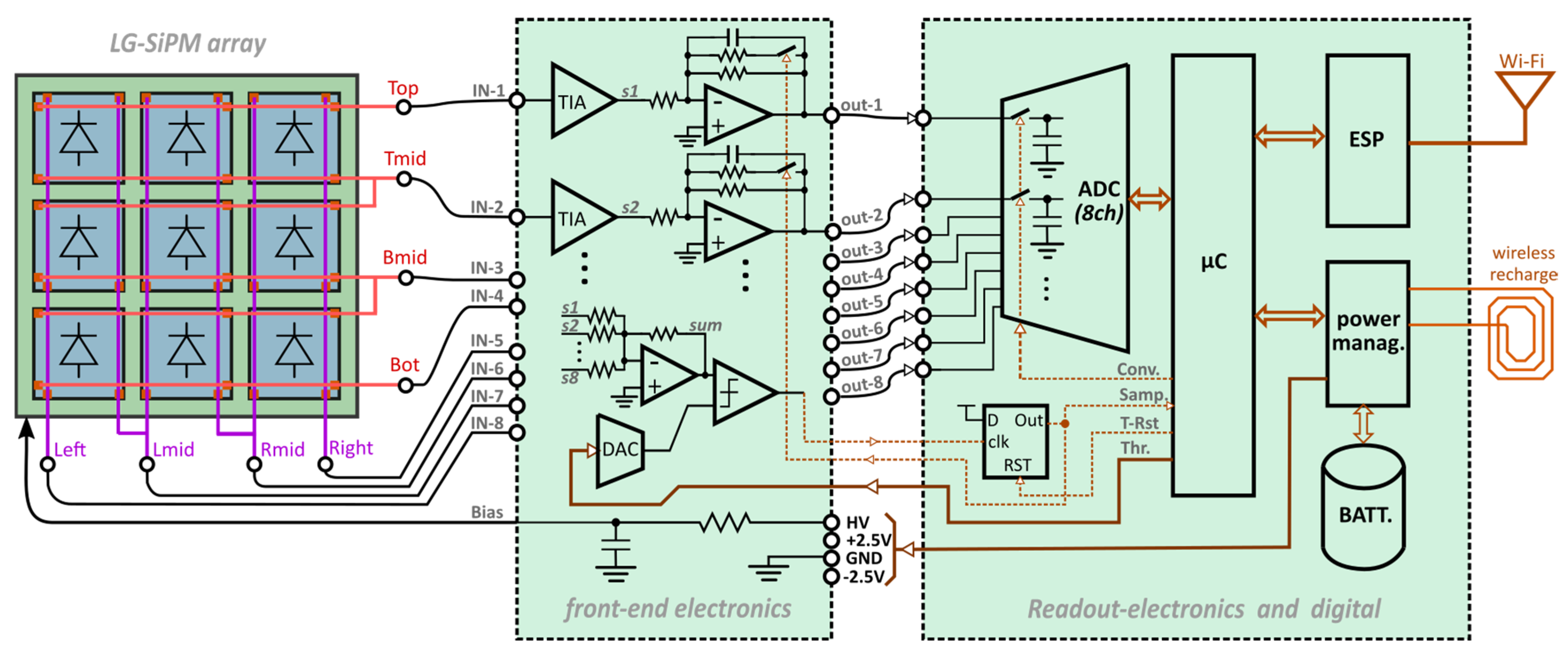
26], we also used the chip array in a “smart-channel configuration” approach, which allowed us to only need 8 readout channels: 4 for the vertical coordinate (named: Top, Tmid, Bmid, and Bot) and 4 for the horizontal coordinate (named: Right, Rmid, Lmid, and Left). The photon absorption position (i.e., corresponding to the emitting pixelated-scintillator element position) is simply calculated as:
Here, the factor 0.33 is used because the signals marked as “mid” are maximum when the position is at one third of the half tile extensions (in positive or negative directions) [
26,
27].
The significant channel reduction allows us to have simple and low-power front-end and readout electronics based on discrete components. A similar channel-reduction concept has been also used in another compact gamma camera implementation (i.e., PGC [
9]), where many SiPM chips, arranged in several commercially available SIPM arrays, have been combined together with a resistive network (all made with discrete components), having 4 output signals at the 4 corners of the network. In our case, the current partitioning is done directly in the LG-SiPM chips, and their output signals are simply connected externally without additional discrete resistors.
3. Camera Design
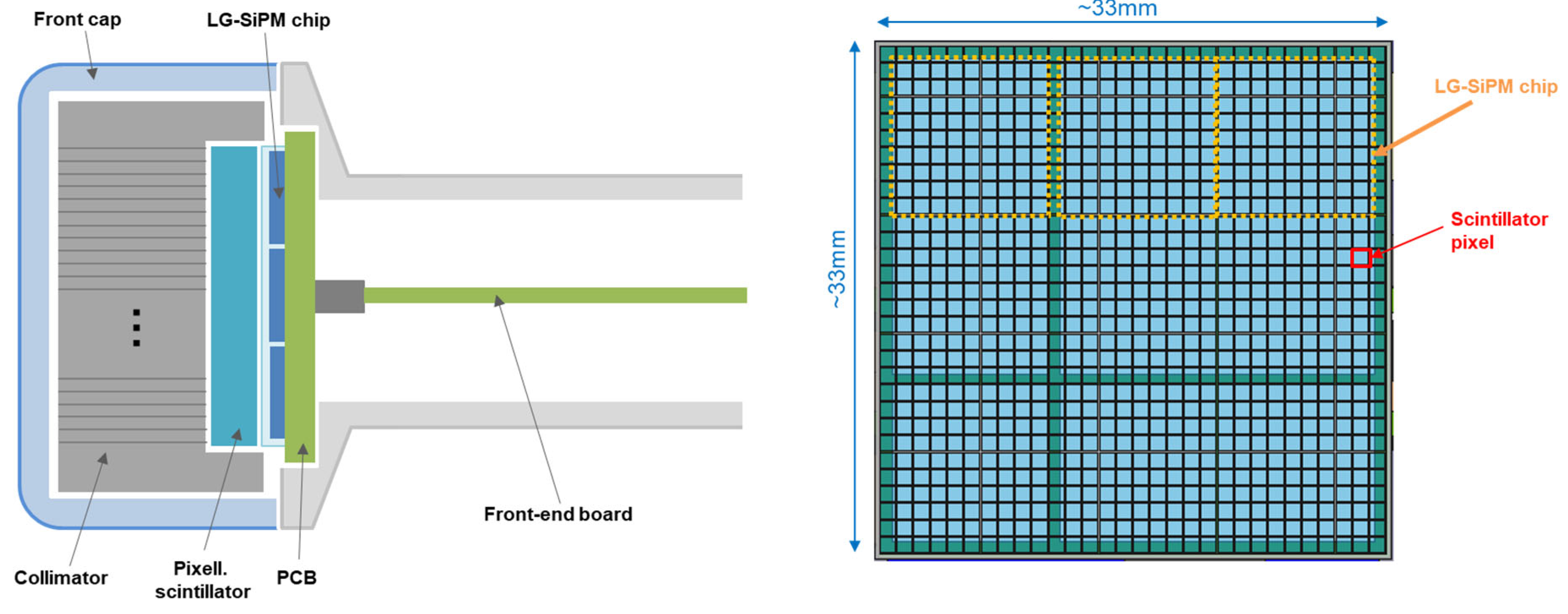
The handheld gamma camera is compact and light (~313–380 g, depending on the collimator mounted, see below). It is composed of three main parts: (i) a front part, including the collimator, the scintillator array, and the SiPM tile; (ii) a central part, including the handle of the camera (made of aluminum) and the front-end electronics; and (iii) the back part, including the readout and digital electronics, the power supply, and the battery (as seen in
Figure 1). The camera is designed to have two collimator options—one shorter (for higher sensitivity in gamma-ray detection but lower spatial resolution) and one longer (for better spatial resolution but smaller sensitivity). Two interchangeable plastic front caps can be used for the two collimator options. The dimensions of the camera are 46 mm × 46 mm × 155 mm in the case of the long collimator. The length is reduced to 147 mm in the case of the short collimator.
The camera is designed to be fully stand-alone and without any cables. Thus, it is based on wireless digital communication with the PC (hosting the graphical user interface, GUI), and it is battery powered. The battery is a lithium–polymer rechargeable battery, with a 2000 mAh capacity, and it is recharged with wireless recharge. The recharge is performed automatically when the camera is placed on the recharge base (see
Figure 1b).
The detection part consists of a parallel-hole collimator, with a septal thickness of 0.2 mm, directly coupled with a pixelated LYSO scintillator (a few millimeters thick, keeping a high photoelectric absorption probability at 140.5 keV). Both are made up of 30 × 30 elements, with a 1.1 mm pitch (total size of almost 33 mm × 33 mm). The collimator is made of tungsten and has >1 mm thick sidewalls that extend towards the scintillator array to shield it from lateral gamma rays (as represented in
Figure 2). The scintillation light is detected by an array of 3 × 3 LG-SiPM chips. Each chip is 10 mm × 10 mm and is wire bonded on two sides (thus, the chips are two-side buttable). To realize a 3 × 3 array, we introduced some extra space in between two of the columns and between two rows, as well at the edges of the tile (see
Figure 2 and [
26]). Because of these spaces, some of the scintillator pixels have a partial light readout, as detailed later. The precise alignment of the collimator, scintillator, and SiPM tile is made with tight tolerances in the front-cap internal space and in the aluminum central body.
As described in the chapter below, the uniformity in sensitivity and the position resolution of the LG-SiPM array is similar to the results presented in [
26]. In particular, it presents a small difference in sensitivity between one chip and the other, and there is a small pincushion effect on the map. To correct such issues, we performed a preliminary calibration on the gamma camera in order to be able to then implement an “energy-correction” and a “position-correction”. These procedures have been implemented in the final camera tests (with scintillator; not with pulsed LED), as detailed in the next chapter.
3.1. Front-End and Readout Electronics
Thanks to the “smart-channel configuration”, the sensor requires only eight readout channels. They must be read out simultaneously in each gamma-ray scintillation event in order to be able to recover the spatial coordinate of the event (i.e., position of the scintillating pixel), calculated with Formula (1), as well as the energy (i.e., total number of scintillating photons). All the SiPM output signals are first amplified with trans-impedance amplifiers (TIAs), with a relatively small gain of ~940 V/A, followed by an approximate integration (see
Figure 3) with variable time constant, as controlled by an analog switch. This is needed in order to integrate the signal during a gamma-ray event but then promptly return following the signal once it has been correctly sampled by the sample and hold (S&H) stage of the analog-to-digital converter (ADC). An alternative solution could be to use a peak stretcher [
39] with a reset after the sampling.
The trigger for the acquisition of the eight signals is provided by a thresholding on the “sum” signal, obtained by the amplified sum of all the signals from the trans-impedance amplifiers. Indeed, depending on the photon flash position, the total charge produced by the SiPM array is split into the 8 channels, but the total charge is always proportional to the gamma-ray energy interacting in the scintillator. Therefore, the thresholding is done on the gamma-ray energy, independent of the position of the scintillating pixel. The threshold voltage is produced by an adjustable digital-to-analog (DAC) converter controlled by the microcontroller, µC (STM32 type).
Once the sum signal overpasses the threshold, a D-type flip-flop circuit (D-FF) is triggered. This sets the approximate integrator in the integrating mode and, at the same time, triggers the µC, which, after an adjustable time interval, starts the sampling and conversion of the ADC. It is important to note that the ADC has eight inputs, and it is able to simultaneously sample them with the same control signal. After the gamma event acquisition, the µC resets the D-FF; thus, the integrator is set back to the signal-following mode. The µC also internally calculates the sum of all the eight signals (“energy” information) and the X and Y coordinates of each event based on Formula (1). To minimize the influences of the offsets in the TIAs, a preliminary manual offset adjustment is performed on the front-end board.
In the readout board, the µC monitors the temperature, the bias voltage, the current absorbed by the SiPMs, the battery status, etc. It is connected with a specific module for WiFi communication (based on an ESP32 module). The ESP32 also implements an HTTP (Hypertext Transfer Protocol) server. The web page is used for: i) quick event mapping; ii) fast status monitoring; and iii) setting the module operating parameters, like the DAC threshold, the delay between the D-FF trigger and the DAC conversion start, etc.
The camera is fully stand-alone. The power supply is provided by the lithium–polymer rechargeable battery, and the power-management board generates the +2.5 V, −2.5 V for the analog part, the 3.3 V for the digital part, and the +5 V for the ADC. The total current absorption is around 0.6 A and thus has a total power consumption of about 1.7 W. This is mainly driven by the analog front-end part that needs to have a moderately high bandwidth (around 100 MHz).
3.2. SPICE Circuital Simulations
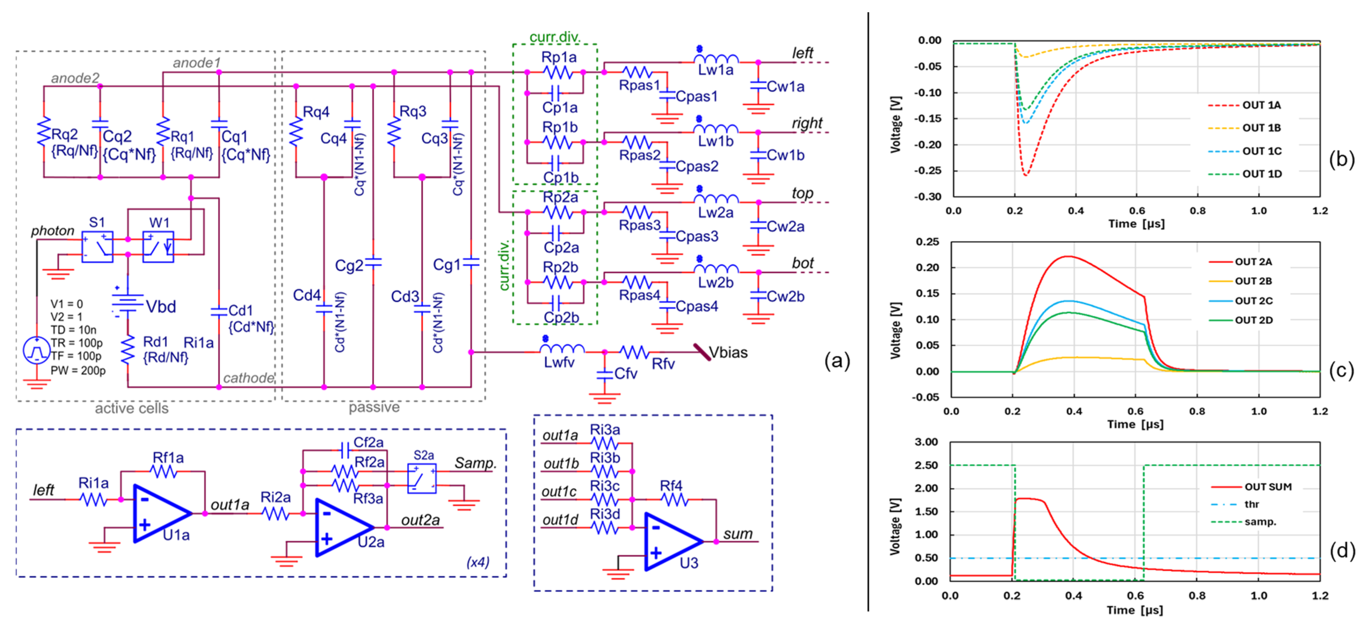
We performed an electrical SPICE simulation of the analog part of the camera circuit in order to check the correct behavior of the front-end electronics. In particular, we wanted to estimate the shape of the pre-amplified signals of the LG-SiPM and to properly dimension the integrator and the triggering logic. We simulated only one LG-SiPM chip, for simplicity, but emulated the capacitance load effect of other chips connected to the same output signal lines with parasitic components.
The SiPM electrical model is based on the “std” SiPM model presented in [
21], but it is extended to the case of four output signals. First, we added a second quenching resistor per each microcell (and quenching capacitance), creating two common anode lines (because, here, it is considered a case of NUV-HD-based technology) (see [
14]). As shown in
Figure 4, the “triggered”-cells part of the SiPM model is the same as in [
21], whereas the “passive”-cells part (i.e., the not-triggered cells) is duplicated in order to have a capacitive load attached to both the first and the second anode lines. These anode lines represent the one going to the vertical and the one to the horizontal current dividers. This is a first-order approximation of the real device, whereas, in reality, this capacitive load is given by all the not-triggered cells, which are connected to both of the cathode lines through their two quenching resistors in each microcell.
Similarly to the model in [
13], the values of Rq1 and Rq2 are given by Rq/Nf (i.e., nominal quenching resistor value divided by the number of triggered cells), whereas Rq3 and Rq4 equal Rq/(N1-Nf) (i.e., nominal Rq divided by N1) and Cq1 and Cq2 equal the nominal Cq value divided by N1-Nf. Differently from the general model, in this case, it has been considered a “local” total number of cells N1, smaller than the total number of cells per chip (N), i.e., only the ones connected to the metal lines sharing the same current divider. These cells are the ones responsible for the capacitive loading effects on the signal. The effect of all the remaining cells (N-N1) is accounted for in the Cpas1, …, Cpas4 capacitances connected after the current divider. Again, this is a first-order approximation of a more complex circuit, where the microcells also interact with each other through the quenching resistors.
The anode1 and anode2 signals are connected to the current dividers, and the resistance of the two branches (Rp1a vs. Rp1b, or Rp2a vs. Rp2b, where Rp1 refers to the first divider and Rp2 to the second) varies depending on the position of the microcells in the chip, with the following relation:
where
Rppar is the equivalent resistance given by the parallel of
Rp1a and
Rp1b. This value is constant in all the branches of the current dividers, i.e., each microcell block sees the same total conductance towards the outside of the chip. In our case, we used an
Rppar of 227 ohm and simulated with an
Rp1a of 250 ohm and an Rp3 of 415 ohm to mimic a condition with very different signal amplitudes in the first divider and similar amplitudes in the second divider.
The signals form the four outputs of the SiPM are amplified by the TIAs, in this case U1x, and are integrated by a second stage (U2x). In the schematic in
Figure 4, we reported just one channel. The second stage has a voltage-controlled switch that can change the integration time constant from the “sampling” mode to the “integration” mode. This is controlled by a comparator stage, followed by a monostable with an adjustable time constant. In the figure, we report an example of the signals from the first TIA blocks (
Figure 4b), as well as the signals after the approximate integrator (
Figure 4c) and the signals after the summing stage and the monostable (
Figure 4d). Note that the integration mode is triggered by a thresholding on the “sum” signal, obtained by an amplified replica of the sum of all TIA outputs. This signal typically saturates in the peak of the signal. This is done in order to have less dependence of the integration starting time on the signal amplitude. In this case, the width is approximately 420 ns; however, in the actual implementation, this time window is adjustable by the user and regulated by the microcontroller timers.
We checked that the signal shapes, the sum signal, and the integration triggering are similar when changing the current divider resistances (maintaining the total conductance and in agreement with Formula (2)). We target an integration time constant of about 290 ns. Thus, given the shape of the signals after the integration stage (
Figure 4c), the proper sampling and conversion start time for the ADC is around 200 ns after the triggering time (i.e., 0.4 µs in
Figure 4c, at the peaking time). This parameter as well can be adjusted by the user in the actual camera. Given the time for triggering, integration, acquisition and conversion in the ADC, the theoretical maximum event rate for the camera is estimated at around 200 kcps (counts per second). However, due to limitations in the serial-interface communication speed and memory usage in the microcontroller, this is limited in practice to around 50 kcps.
4. Performance Evaluation
The POSICS2 gamma camera has been tested in terms of functionality, position resolution with LED illumination (i.e., without a scintillator and collimator on top) and with a point-like gamma source, measuring the sensitivity, energy resolution, and position resolution (with a scintillator and collimator on top).
For the tests with LED illumination, the camera has been mounted on two-stage micro-positioners and placed inside a light-tight climatic chamber set at 20 °C (
Figure 5a). The back enclosure has been removed to be able to extract the analog signals from test points on the board. In the examples shown in
Figure 5, we split the eight analog signals at the output from the approximated integrator into two, with one path going to the ADC and the other one being connected outside the chamber to two synchronized oscilloscopes (four channels each, as done in [
26]). In
Figure 5b, we show examples of signals in the case of “samp” signal triggering inhibited, whereas in
Figure 5c, we show examples of the relative signals with the event triggering active, both in the case of illumination in the upper-left region of the sensor tile. It can be seen that with event triggering, the signals have a higher amplitude but slower rising edges. It can also be seen that there is a small interference by the digital signals on the analog lines, in two time positions, due to the comparator output switching; however, this does not interfere with the ADC data conversion.
In the characterization setup, the camera was battery powered and continuously communicating through WiFi with the PC outside the chamber. The camera was controlled and monitored with a custom-made HTML interface, where it was possible to set the acquisition mode (e.g., continuous updating, with fixed time interval, or “start–stop”, controlled with the switch on the camera, etc.) and the working parameters through endpoints.
We characterized the position resolution through the analog signals acquired with the oscilloscopes (as done in [
26]) and with the “event data” acquired digitally from the camera through WiFi communication. Indeed, the camera was continuously acquiring the gamma-ray events, i.e., every time the “samp” signal triggered the microcontroller, it triggered the ADC and acquired the eight signals. For each acquired event, the microcontroller calculated the event position through Formula (1) and stored thousands of events in terms of both the “raw data” (i.e., ADC data of the eight channels) and the “event data” (i.e., position X, Y, and SUM values). These values could be downloaded by the PC through proper endpoints.
4.1. Test of the Front-End Electronics
The position resolution was first characterized with pulsed LED illumination, with a procedure like the one used to characterize the LG-SiPM array in [
26], using only the analog signals. This test was used to evaluate the sensor and the analog front end of the camera. We acquired the signals at the output of the amplifiers, integrating the signals around the main peak for a time window of 150 ns. The sensor was biased at 4 V of excess bias and scanned with a 1.5 mm step. The intensity was around 300 detected photons per pulse. In each position, we acquired 256 events and included the reconstructed positions in the map, as shown in
Figure 6a. It can be seen that all the points are well distinguishable and with a good position resolution of about σ = 180 µm ÷ 200 µm (considering only the active region of the SiPM array).
Then, we mounted the scintillator array, and we acquired a map of the reconstructed positions using a uniform emission from a Tc-99m source (40 MBq). The scintillator pixels illuminated the SiPM tile as schematized in
Figure 2, having a pitch of 1.1 mm. In
Figure 6b, we report the obtained map considering all the events without discrimination on gamma-ray energy, whereas in
Figure 6c, we report the map of only the events in the photopeak, i.e., ~140 keV, discarding the lower energy events (120–160 keV energy window). The energy is estimated by the sum of all signal amplitudes. In both cases, the shape of the map is similar to the one with LED illumination, showing a similar pincushion effect (as also described in [
26]). All the points are well distinguishable, with better position resolution when discarding the lower energy events (which create a shadowing towards the central position).
4.2. Full-Camera Tests
We performed full-camera tests, i.e., with the camera closed and operating as in the real environment. Although it was still mounted on the micro-positioning stages, it was closed, battery powered, and communicating only with the WiFi interface.
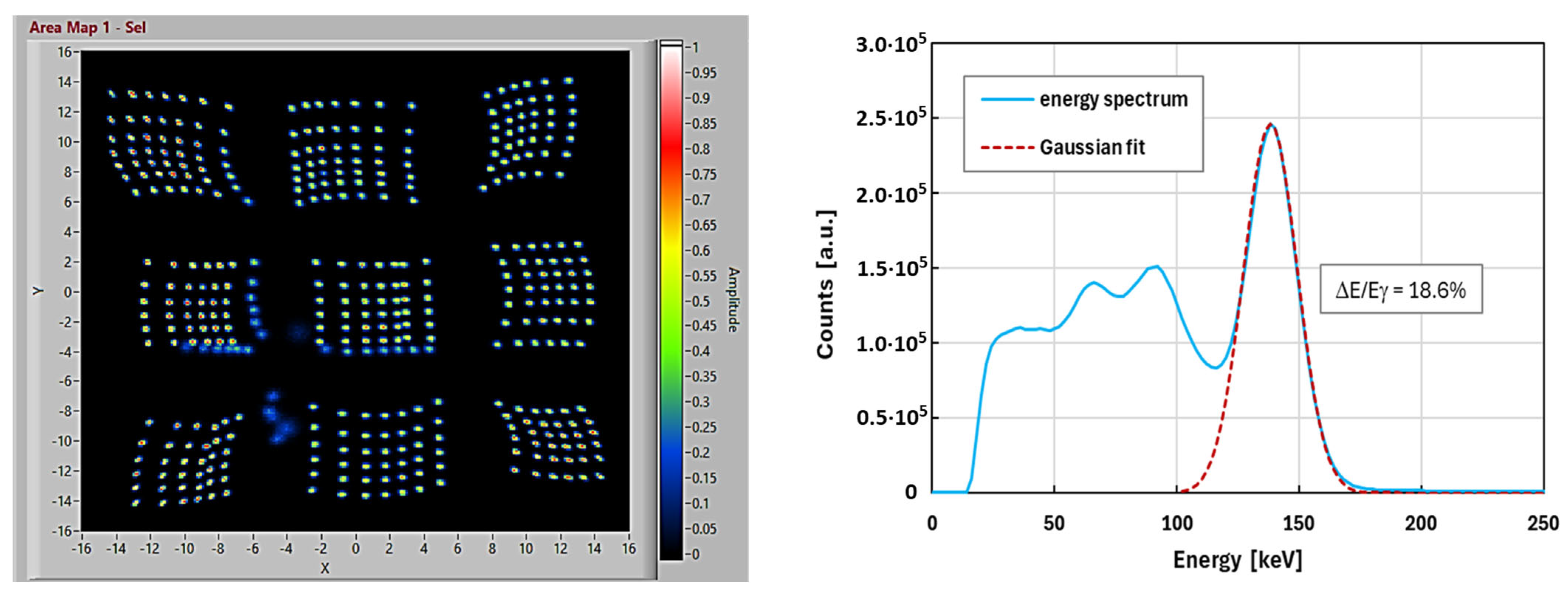
We evaluated the position resolution again with pulsed LED illumination directly on the sensor tile, with the same bias of the sensor, the same scan step, and a similar light intensity. In each scan position, we acquired 4000 events from the camera. The LED repetition rate was 5 KHz. As can be seen in
Figure 7(left), the points are still clearly visible with the estimated resolution in the position of σ = 185 µm ÷ 205 µm, indicating that the digital acquisition in the gamma camera gives results similar to the acquisition done with the oscilloscopes. In this case, we can have some artifacts (see figure) due to illumination spots completely in not-sensitive regions (because the LED spot is small, i.e., ~200 µm)
Then, we characterized the camera with the scintillator array and the collimator (short one) mounted when detecting the gamma ray from a Tc-99m flat-field phantom (40 Mbq source), thus uniformly illuminating all the sensitive areas. We estimated the energy resolution of the camera after performing the “energy-correction” algorithm. This is necessary to compensate all the minor variations in signal amplitude between SiPM chips (due to gaps between SiPM chips and due to minor series resistances and parasitics). The results are shown in
Figure 7(right). We obtained an energy resolution of about 18.6% FWHM at the 140 keV peak.
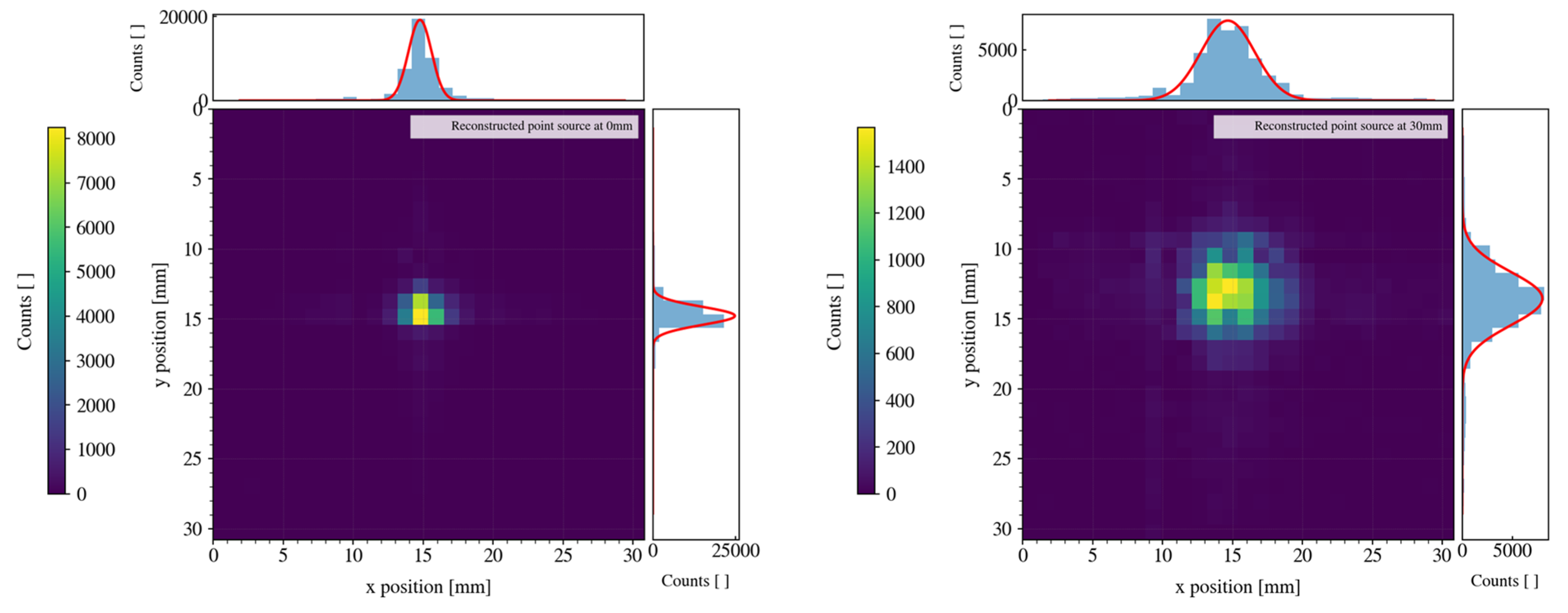
Finally, we tested the spatial resolution of the camera by directly detecting the emission of an almost-point-source of Co-57 (activity of about 3 MBq) placed in front of the cap of the camera at a distance equal to 0 mm and at a 30 mm distance (see
Figure 8). As expected, with a parallel-hole collimator with moderate septal thickness, the resolution worsens when the source is more distant from the collimator. We estimated a spatial resolution of ~1.9 mm FWHM in the case of a 0 mm distance, and 5.1 mm FWHM in the case of a 30 mm distance. We also measured the sensitivity of the gamma camera, with the point source at a 2 mm distance, as being ~1444 cps/MBq when collecting all the events without energy discrimination and being ~481 cps/MBq when discriminating only the events in the photopeak (i.e., 120–160 keV energy window), as summarized in
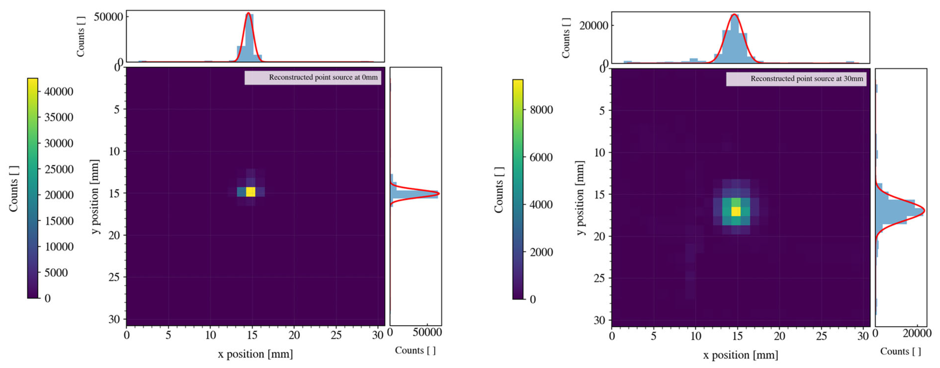
Table 1. Note that these measurements were done using the shorter collimator—the one made to have higher sensitivity and lower spatial resolution. We also tested the camera with the second type of collimator—the longer one. In similar conditions as the ones described above, we obtained a spatial resolution of 1.4 mm FWHM when the point source was at a 0 mm distance and 2.8 mm FWHM in the case of a 30 mm distance (see
Figure 9). The better performance in terms of resolution was expected because of the smaller acceptance angle for the gamma rays of the collimator. On the contrary, this reflects on a smaller sensitivity of about 730 cps/MBq and of ~134 cps/MBq when collecting all the events or when selecting only the one with energy in the photopeak, respectively.
5. Conclusions
We developed and tested a novel compact (i.e., ~150 mm × 48 mm × 48 mm), light, low-power (~1.7 W total), wireless, handheld gamma camera developed for radio-guided surgery. This camera is based on a particular position-sensitive Silicon Photomultiplier (SiPM technology), namely the FBK linearly graded SiPM (LG-SiPM) technology. The detector is made up of a 3 × 3 array of 10 × 10 mm2 SiPM chips having an area of about 31 × 31 mm2. Thanks to this detector technology, it is possible to significantly reduce the number of readout channels to just eight, reducing the complexity and lowering the power consumption of all the readout electronics. The novel gamma camera is light (~313 ÷ 380 g, all included), battery powered, and compact. Compared with other implementations, we focused on having a completely stand-alone system with WiFi communication and wireless recharge.
We performed electrical simulations of the detector and the front-end electronics, extrapolating the signal shapes and amplitude. This allowed us proper dimensioning of the amplification gains and integration time constant. We mounted and tested the first camera prototype, including a pixelated fine-pitch (1.1 mm) LYSO crystal array, and a couple of interchangeable parallel-hole tungsten collimators (longer or shorter length, for better position resolution or sensitivity, respectively).
The detection area and the field-of-view (FoV), as well as the energy and spatial resolution, are comparable with the average functions of other state-of-the-art implementations. We measured the performance of the gamma camera with a Tc-99m flat-field phantom (40 Mbq source), obtaining an energy resolution of about 18% FWHM at the 140 keV peak. We measured the spatial resolution performance of the camera with a Co-57 point-source, obtaining 1.9 mm FWHM in the case of a 0 mm distance from the source to the front cap of the camera and obtained 5.1 mm FWHM in the case of a 30 mm distance with the short collimator option mounted. On the contrary, we obtained 1.4 mm FWHM and 2.8 mm FWHM for distances of 0 and 30 mm, respectively, when mounting the longer collimator. The corresponding sensitivity (measured with the source at a 2 mm distance) is ~1444 cps/MBq without any energy discrimination (~481 cps/MBq taking only the events in the photopeak, around 140 keV) and ~730 cps/MBq without any energy discrimination (~134 cps/MBq taking only the events in the photopeak), respectively, for the two collimators.
These promising results place the reported gamma camera among the state-of-the-art solutions, especially in terms of weight, compactness, usability and performance, paving the way for many new practices that can be used in the operating room by surgeons in order to be able to excise tumors with greater precision and greater awareness of their shape and location.

