
Multichannel Time Synchronization Based on PTP through a High Voltage Isolation Buffer Network Interface for Thick-GEM Detectors

 ,
,  ,
,  , , , and
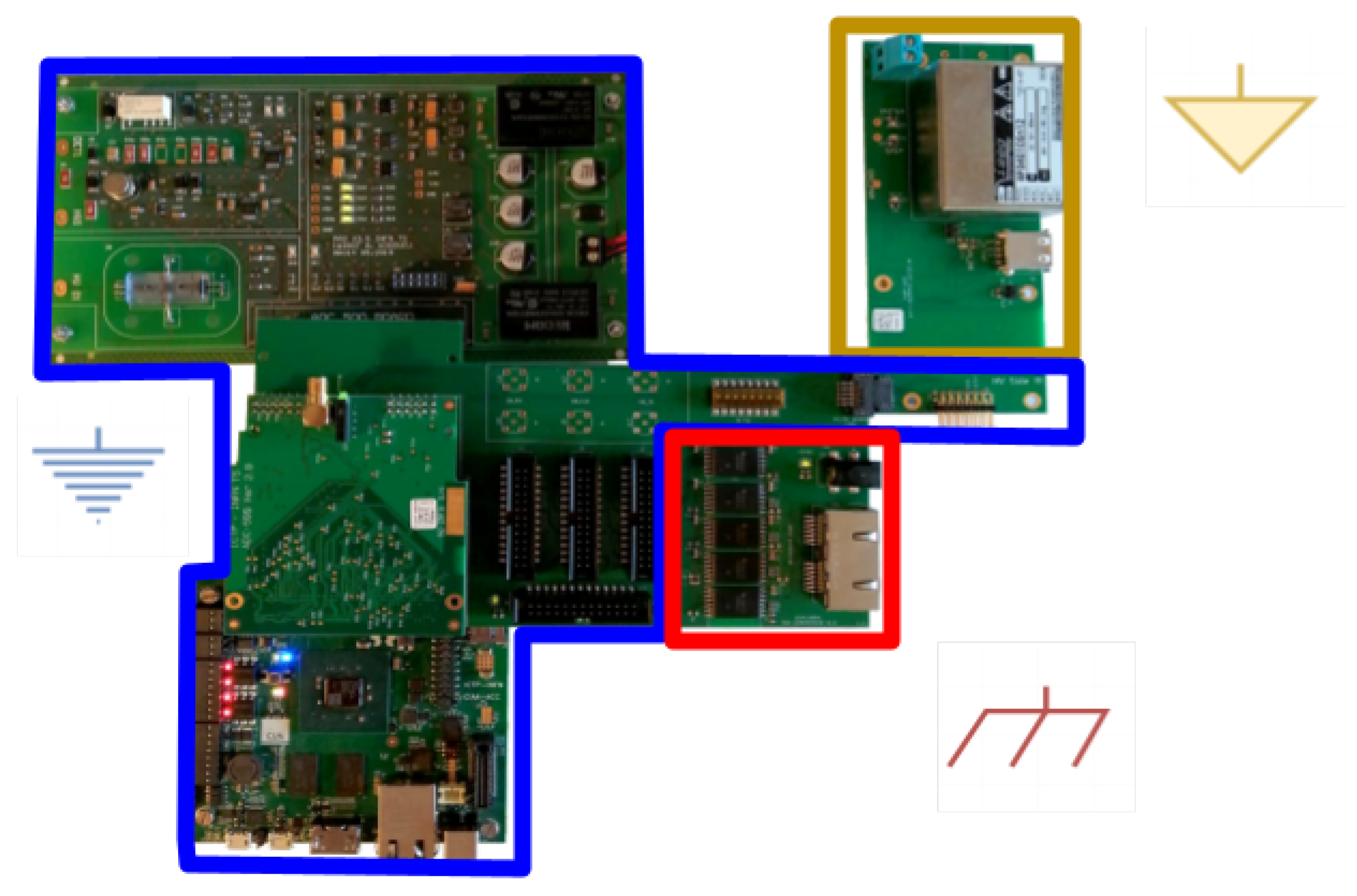
Abstract
:1. Introduction
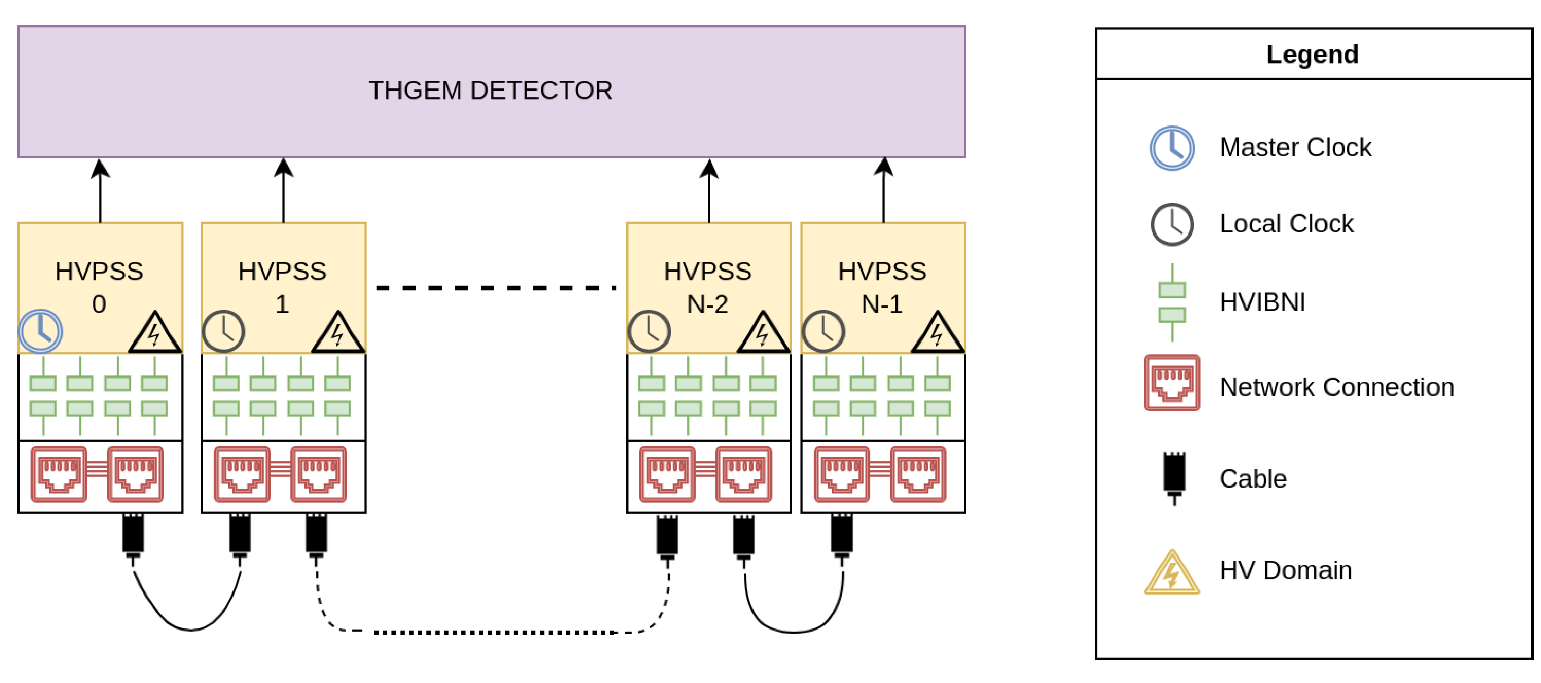
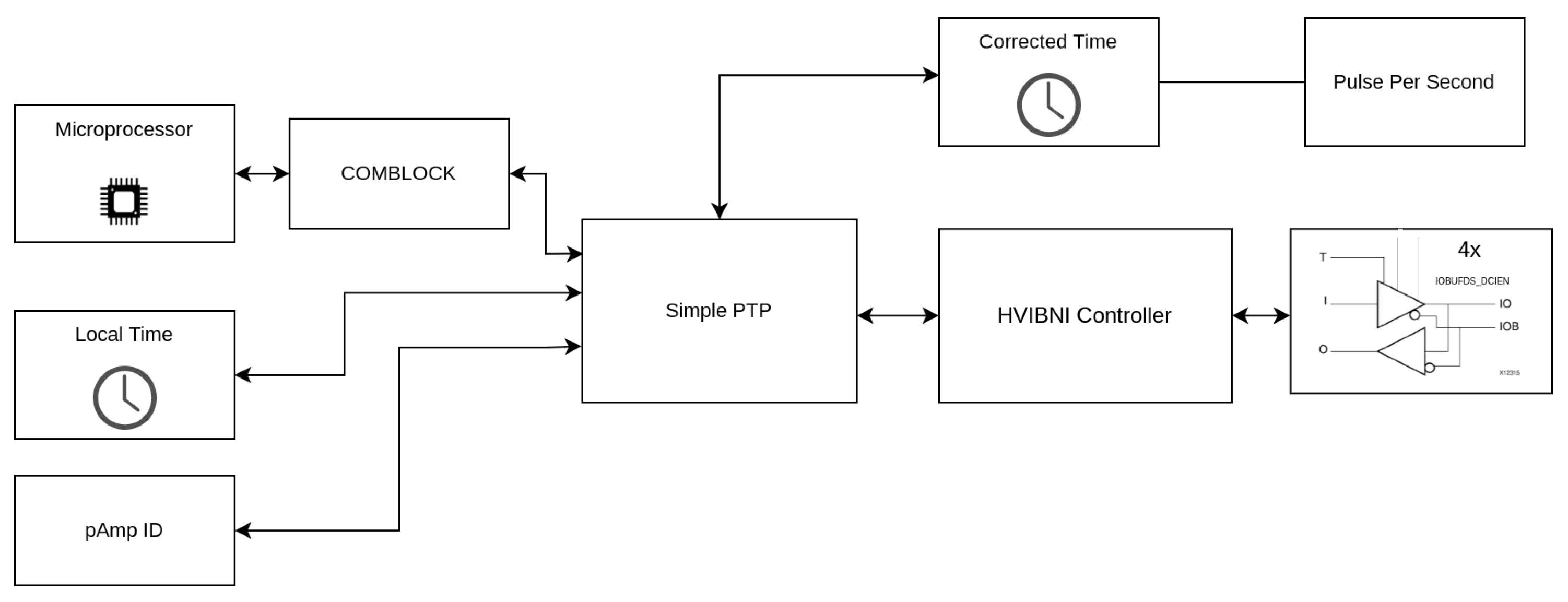
2. System Description and Topology
- Picoammeter system (blue): Comprised by a picoammeter board, a high speed 500 MHz ADC08500.
- HV DC-DC Converter (yellow): Comprised by a ISEG BPS-Family 4W power supply, 16 bits DAC for HV-setup, and 18 bits current and voltage monitoring (IMON, VMON correspondingly).
- Network Interface (red): Comprised by four High Voltage Isolated Bidirectional Network Interface (HVIBNI) connected to two RJ45 female connectors.
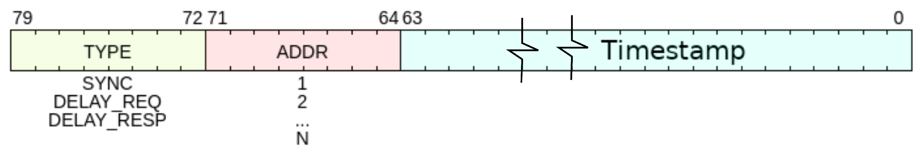
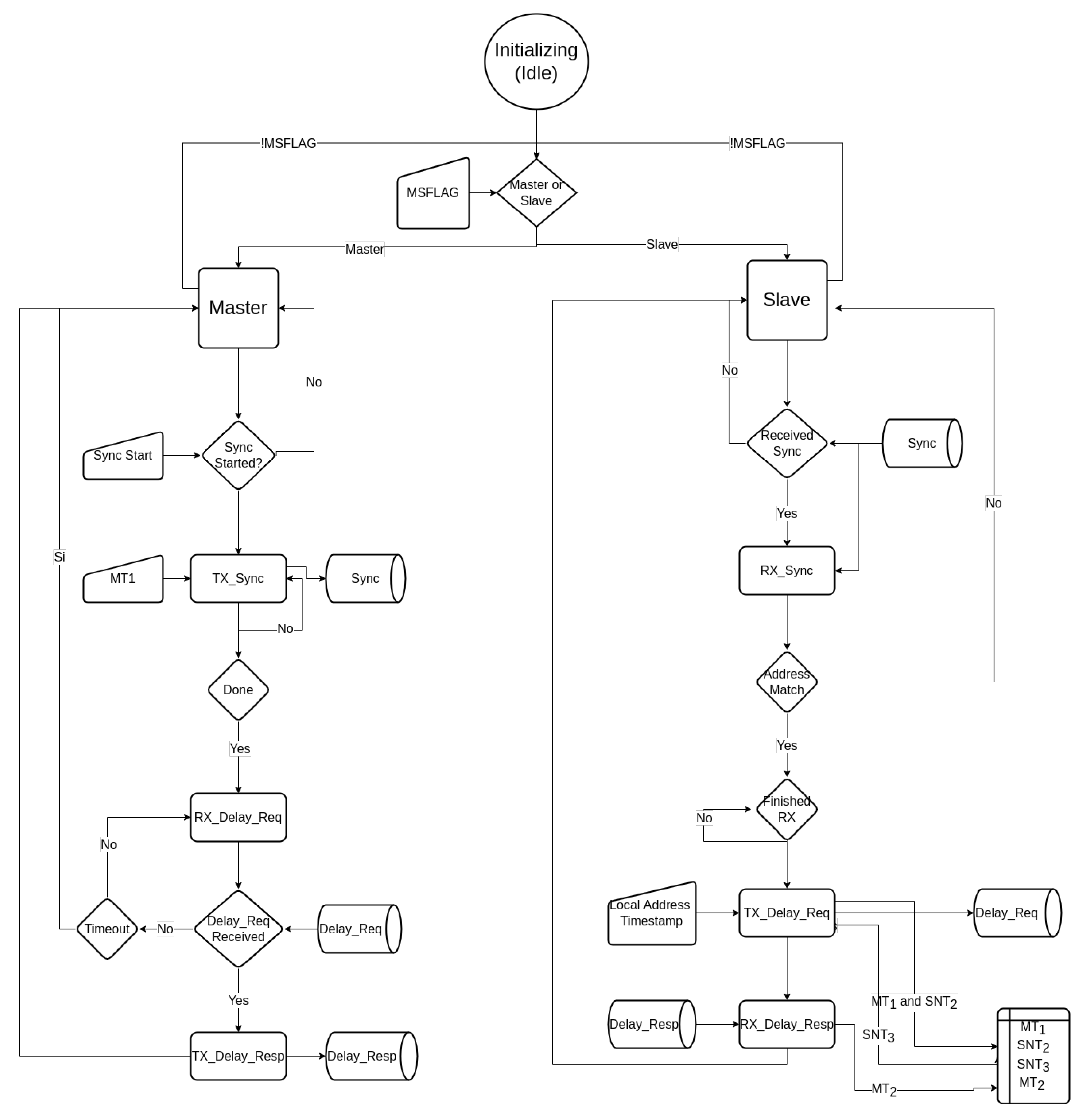
3. Simplified PTP Synchronization Scheme
- The master sends a Sync signal, its address, and the timestamp to the slave N in a single package. All the slaves take a timestamp as soon as the Sync signal arrives, which is kept until the address is validated. The time is then stored in the intended slave for synchronization;
- In a time , the slave sends a Delay Request to the master. The master takes a timestamp as soon as the request is received;
- The master sends the timestamp to the slave with a header Delay Response, opening the communication channel;
- The slave calculates the time correction using the obtained information.
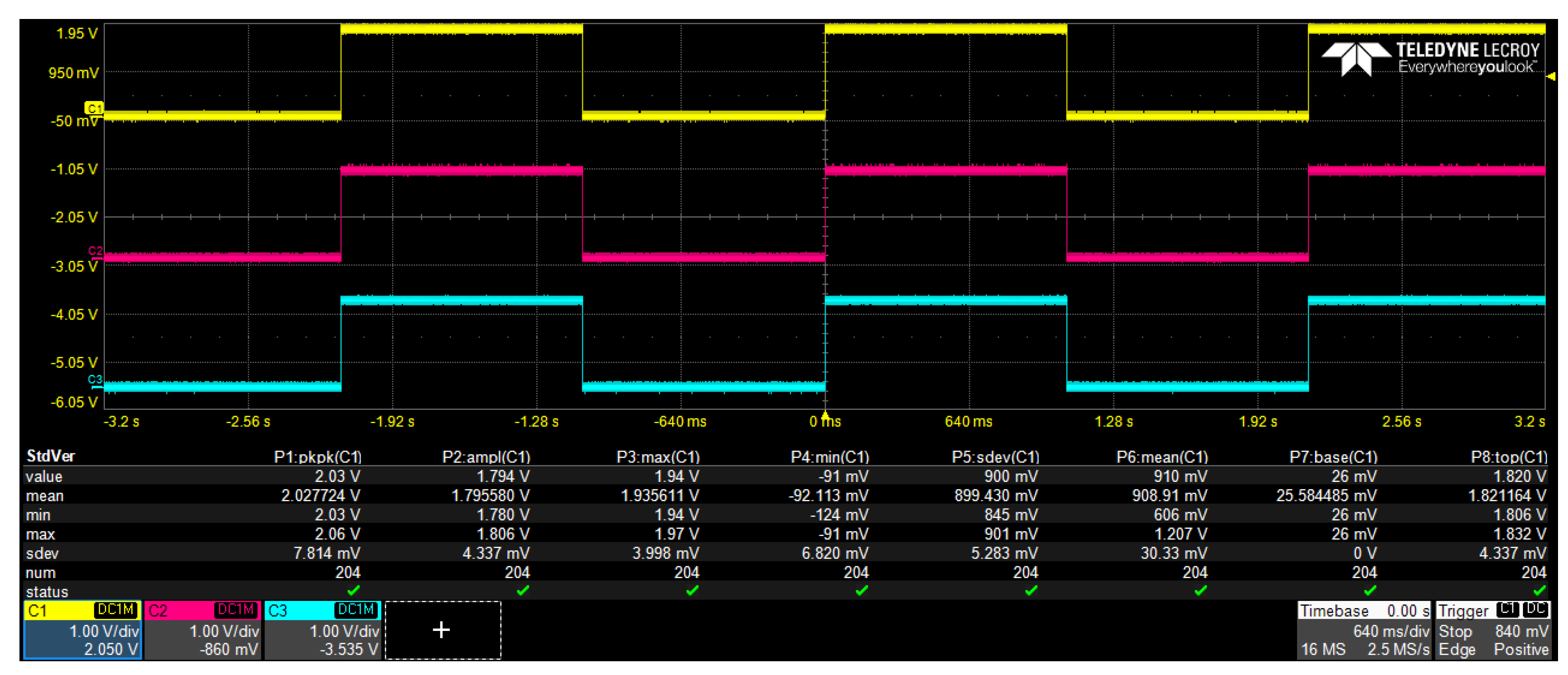
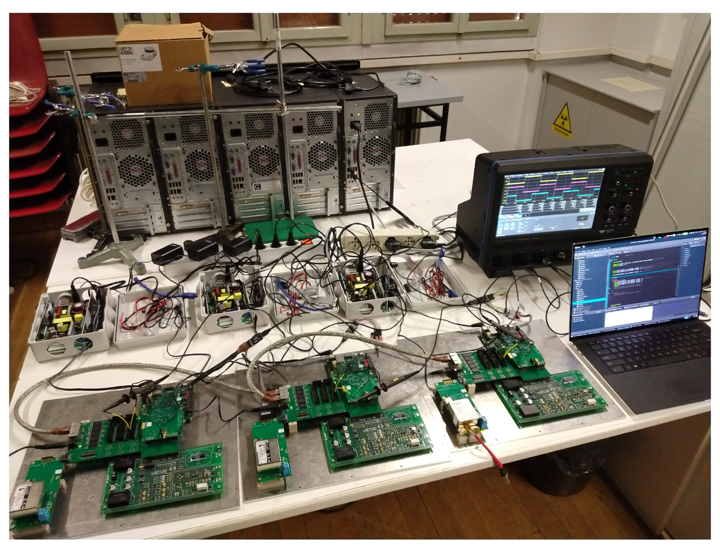
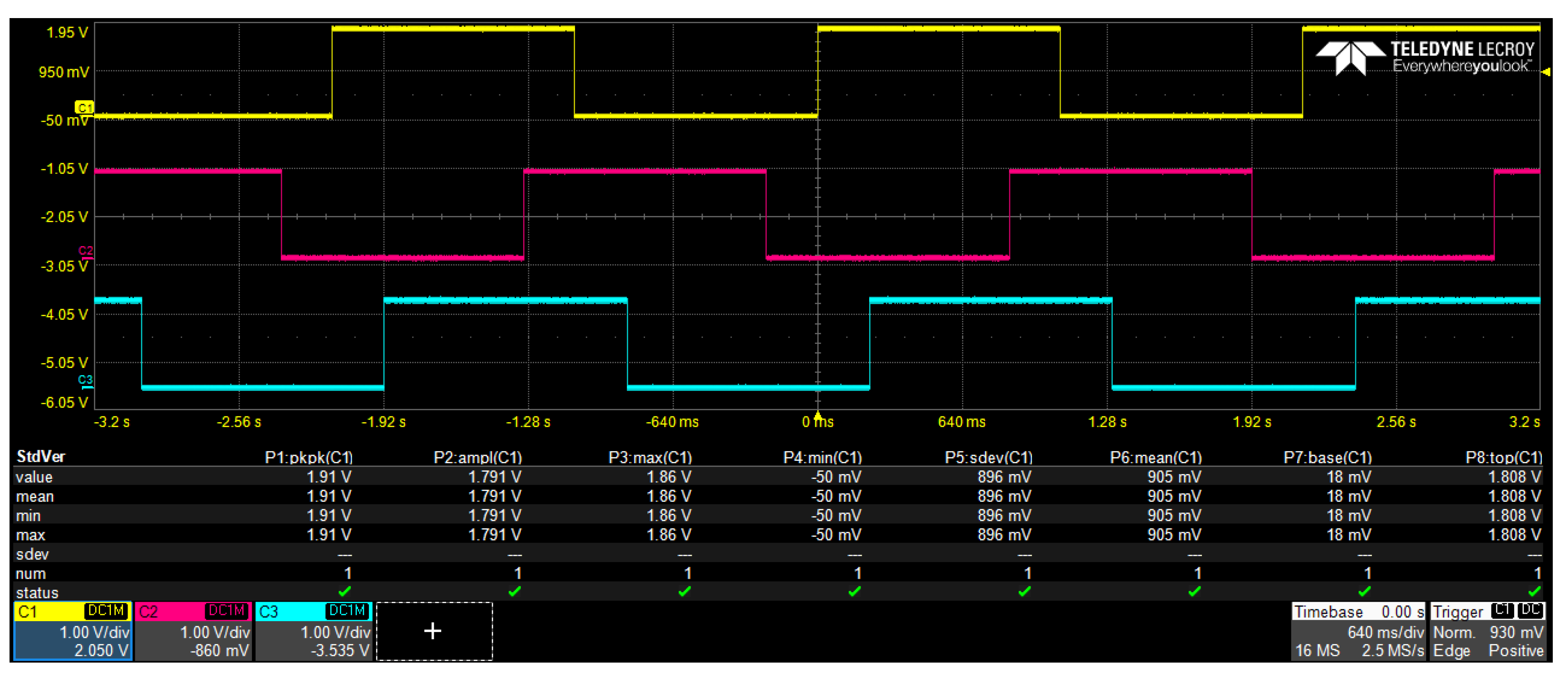
4. Experimental Setup and Results
5. Discussion
6. Conclusions and Future Works
Author Contributions
Funding
Institutional Review Board Statement
Informed Consent Statement
Data Availability Statement
Acknowledgments
Conflicts of Interest
Abbreviations
| CIAA-ACC | Computadora Industrial Abierta Argentina |
| CTIME | Correction Time |
| CTRDY | Correction Ready |
| DAC | Digital to Analog Converter |
| DC | Direct Current |
| FPGA | Field-Programmable Gate Array |
| HV | High Voltage |
| HVIBNI | High Voltage Isolated Bidirectional Network Interface |
| HVPSS | High Voltage Power Supply System |
| ILA | Integrated Logic Analyzer |
| JTAG | Joint Test Action Group |
| MICROMEGAS | Micro-Mesh Gaseous Structure |
| MLAB | Multidisciplinary Laboratory |
| MPGD | Micro Pattern Gaseous Detector |
| MSFLAG | Master Setup Flag |
| MT | Master clock Time |
| pAmp | Pico-Amperometer |
| PCB | Printer Circuit Board |
| PPS | Pulse-Per-Second |
| PTP | Precise Time Protocol |
| RTL | Register-transfer-level |
| SNT | Slave N clock Time |
| SoC | System-on-Chip |
| THGEM | Thick Gaseous Electron Multipliers |
| UART | Universal Asynchronous Receiver-Transmitter |
| VHDL | Very High-Speed Integrated Circuit Hardware Description Language |
References
- Sauli, F. Micro-Pattern Gaseous Detectors: Principles of Operation and Applications; World Scientific: Singapore, 2021. [Google Scholar]
- Chechik, R.; Breskin, A.; Shalem, C.; Mormann, D. Thick GEM-like hole multipliers: Properties and possible applications. Nucl. Instrum. Methods Phys. Res. Sect. Accel. Spectrometers Detect. Assoc. Equip. 2004, 535, 303–308. [Google Scholar] [CrossRef]
- Agarwala, J.; Bari, M.; Bradamante, F.; Bressan, A.; Chatterjee, C.; Cicuttin, A.; Ciliberti, P.; Crespo, M.; Torre, S.D.; Dasgupta, S.; et al. The high voltage system with pressure and temperature corrections for the novel MPGD-based photon detectors of COMPASS RICH-1. Nucl. Instrum. Methods Phys. Res. Sect. Accel. Spectrometers Detect. Assoc. Equip. 2019, 942, 162378. [Google Scholar] [CrossRef] [Green Version]
- Carrato, S.; Chatterjee, C.; Cicuttin, A.; Ciliberti, P.; Crespo, M.; Dalla Torre, S.; Dasgupta, S.; Florian, W.; Ordóñez, L.G.; Gobbo, B.; et al. A scalable High Voltage Power Supply System with system on chip control for Micro Pattern Gaseous Detectors. Nucl. Instrum. Methods Phys. Res. Sect. Accel. Spectrometers Detect. Assoc. Equip. 2020, 963, 163763. [Google Scholar] [CrossRef]
- Levorato, S. A scalable High Voltage power supply system with SoC control for Micro Pattern Gaseous Detector. In Proceedings of the 6th International Conference on Micro Pattern Gaseous Detectors, MPGD19, La Rochelle, France, 5–10 May 2019. [Google Scholar]
- García, L.G.; Crespo, M.L.; Carrato, S.; Cicuttin, A.; Florian, W.; Molina, R.; Valinoti, B.; Levorato, S. High Voltage Isolated Bidirectional Network Interface for SoC-FPGA Based Devices. In Applications in Electronics Pervading Industry, Environment and Society; Saponara, S., De Gloria, A., Eds.; Springer International Publishing: Cham, Switzerland, 2021; pp. 280–285. [Google Scholar]
- IEEE Std 1588-2019 (Revision of IEEE Std 1588-2008); IEEE Standard for a Precision Clock Synchronization Protocol for Networked Measurement and Control Systems. Institute of Electrical and Electronics Engineers: New York, NY, USA, 2020; pp. 1–499. [CrossRef]
- INTI. CIAA ACC Hardware User Guide. 2021. Available online: https://github.com/ciaa/CIAA_ACC/blob/master/doc/user_guide.md (accessed on 18 December 2021).
- ISEG. BPS Series, Small High Voltage Module for PCB Mounting Up to 4 Watt; ISEG Spezialelektronik GmbH: Radeberg, Germany, 2021. [Google Scholar]
- Texas Instruments. ISO782xLL High-Performance, 8000-VPK Reinforced Isolated Dual-LVDS Buffer, sllset8a ed.; Texas Instruments Incorporated: Dallas, TX, USA, 2016; Revision A. [Google Scholar]
- Texas Instruments. ISO7840x High-Performance, 8000-VPK Reinforced Quad-Channel Digital Isolator, sllsen2b ed.; Texas Instruments Incorporated: Dallas, TX, USA, 2015; Revision B. [Google Scholar]
- ICTP MLAB; INTI CMNT. The Core Comblock. 2021. Available online: https://gitlab.com/rodrigomelo9/core-comblock (accessed on 18 December 2021).
- Lipiński, M.; Włostowski, T.; Serrano, J.; Alvarez, P. White rabbit: A PTP application for robust sub-nanosecond synchronization. In Proceedings of the 2011 IEEE International Symposium on Precision Clock Synchronization for Measurement, Control and Communication, Munich, Germany, 12–16 September 2011; pp. 25–30. [Google Scholar] [CrossRef]


Publisher’s Note: MDPI stays neutral with regard to jurisdictional claims in published maps and institutional affiliations. |
© 2022 by the authors. Licensee MDPI, Basel, Switzerland. This article is an open access article distributed under the terms and conditions of the Creative Commons Attribution (CC BY) license (https://creativecommons.org/licenses/by/4.0/).
Share and Cite
García Ordóñez, L.G.; Crespo, M.L.; Carrato, S.; Cicuttin, A.; Florian Samayoa, W.O.; D’Ago, D.; Levorato, S. Multichannel Time Synchronization Based on PTP through a High Voltage Isolation Buffer Network Interface for Thick-GEM Detectors. Instruments 2022, 6, 11. https://doi.org/10.3390/instruments6010011
García Ordóñez LG, Crespo ML, Carrato S, Cicuttin A, Florian Samayoa WO, D’Ago D, Levorato S. Multichannel Time Synchronization Based on PTP through a High Voltage Isolation Buffer Network Interface for Thick-GEM Detectors. Instruments. 2022; 6(1):11. https://doi.org/10.3390/instruments6010011
Chicago/Turabian StyleGarcía Ordóñez, Luis Guillermo, Maria Liz Crespo, Sergio Carrato, Andres Cicuttin, Werner Oswaldo Florian Samayoa, Daniele D’Ago, and Stefano Levorato. 2022. "Multichannel Time Synchronization Based on PTP through a High Voltage Isolation Buffer Network Interface for Thick-GEM Detectors" Instruments 6, no. 1: 11. https://doi.org/10.3390/instruments6010011
APA StyleGarcía Ordóñez, L. G., Crespo, M. L., Carrato, S., Cicuttin, A., Florian Samayoa, W. O., D’Ago, D., & Levorato, S. (2022). Multichannel Time Synchronization Based on PTP through a High Voltage Isolation Buffer Network Interface for Thick-GEM Detectors. Instruments, 6(1), 11. https://doi.org/10.3390/instruments6010011