Article

Microwave Field-Induced Changes in Raman Modes and Magnetic Force Images of Antiferromagnetic NiO Films

1
Departamento de Física de la Materia Condensada C-03, Universidad Autónoma de Madrid, 28049 Madrid, Spain
2
Departamento de Electrocerámica, Instituto de Cerámica y Vidrio (ICV), Consejo Superior de Investigaciones Científicas (CSIC), 28049 Madrid, Spain
3
Instituto Nicolás Cabrera (INC), Universidad Autónoma de Madrid, 28049 Madrid, Spain
4
Condensed Matter Physics Institute (IFIMAC), Universidad Autónoma de Madrid, 28049 Madrid, Spain
5
Departamento de Física Aplicada C-12, Universidad Autónoma de Madrid, 28049 Madrid, Spain
6
Departamento de Física Teorica de la Materia Condensada C-05, Universidad Autónoma de Madrid, 28049 Madrid, Spain
*
Author to whom correspondence should be addressed.
Condens. Matter 2024, 9(1), 7; https://doi.org/10.3390/condmat9010007
Submission received: 29 September 2023 / Revised: 27 November 2023 / Accepted: 2 January 2024 / Published: 15 January 2024

Abstract

:
Effective control of domain walls or magnetic textures in antiferromagnets promises to enable robust, fast, and nonvolatile memories. The lack of net magnetic moment in antiferromagnets implies the need for creative ways to achieve such a manipulation. We conducted a study to investigate changes in magnetic force microscopy (MFM) imaging and in the magnon-related mode in Raman spectroscopy of virgin NiO films under a microwave pump. After MFM and Raman studies were conducted, a combined action of broadband microwave (0.01–20 GHz, power scanned from 20 to 5 dBm) and magnetic field (up to 3 kOe) were applied to virgin epitaxial (111) NiO and (100) NiO films grown on (0001) Al 2 O 3 and (100) MgO substrates, following which the MFM and Raman studies were repeated. We observed a suppression of the magnon-related Raman mode subsequent to the microwave exposure. Based on MFM imaging, this effect appeared to be caused by the suppression of large antiferromagnetic domain walls due to the possible excitation of antiferromagnetic spin oscillations localized within the antiferromagnetic domain walls.

1. Introduction

Recently, antiferromagnets (AFMs) and particularly insulating thin AFM films have attracted considerable attention due to their potentially unmatched characteristics, which could allow the development of spintronic devices with speeds reaching the THz domain [1,2], ultralow Gilbert damping [3], and good spin current conduction [4]. Another unique merit of AFMs is the minuteness of the stray fields [5] and consequently, the difficulty in controlling the domain walls (AFM DWs) with laboratory magnetic fields. The presence of AFM DWs may substantially restrict the propagation length of magnons in antiferromagnets [6]. The effective manipulation of magnetic textures in antiferromagnets, and specifically those related to AFM DWs, is central to the emerging field of AFM spintronics [7].
A number of schemes to control the AFM DWs have been proposed recently. Among them are thermal [8] or strong field gradients [9] and field pulses [10] or spin waves [11] with specific helicity [12]. Néel spin torque to drive AFM DWs should be effective only for specific antiferromagnets with locally broken inversion symmetry [13]. The practical realization of this mechanism via electrical switching of antiferromagnets with (high energy loss) DC currents [14] has been under debate [15,16]. Robust control over AFM DWs, which is critical for effective spin wave propagation over micrometer distances [6], still remains a significant challenge [13], and alternative techniques are required to probe and manipulate nontrivial AFM order [5].
NiO is an archetype antiferromagnet for room-temperature applications, and has recently been the focus of intensive research, as it shows AFM resonance in the THz range in the absence of a external magnetic field [17,18], which nonetheless could be tuned by an external field of a few Tesla [19]. In the last few years, there have been some proposals involving the exploration of THz spin dynamics with the aim of creating AFM memories [20,21]. However, the domain structure of NiO is very complex, as at least 12 orientation domains including twin (T) and spin (S) domains [22] and double domain walls [23] have been reported, with sizes of about microns to tenths of a micron depending on the oxygen annealing conditions [24].
Interestingly, recent studies have revealed that spin current transmission in AFM insulators can be mediated by coherent spin waves not only in THz [25] but also in the GHz range [26,27]. This observation confirms previous reports on spin angular momentum transfer at the GHz excitation range without phase control [28,29,30,31] and inertial dynamics of antiferromagnets [32]. The GHz dynamics of solitons or AFM DWs [11] could be excited either by circular or linearly polarized drives capable of producing a net AFM DW drift in colinear antiferromagnets [33,34]. Besides evanescent [27] and thermal spin waves [4,31,35,36] underlying the spin transport through AFMs, another intriguing possibility for low-frequency spin waves’ propagation exists due to the modes localized around the domain walls [37].
Recently, laser pulses have been shown to be capable of modifying the structure of AFM DWs, creating antiferromagnetic 180 domains in NiO/Pt bilayers [38]. In this study, we investigated the possibility of influencing the AFM DW structure in virgin NiO films via the application of broadband (10 MHz–20 GHz) microwaves (MW) with a power up to 5 dBm and an in-plane magnetic field up to 3 kOe at room temperature. We used magnetic force microscopy and confocal micro-Raman spectroscopy to study the possible effect of the microwave excitation on the AFM DW magnetic textures in NiO.

2. Structural Characterization of the Virgin Films

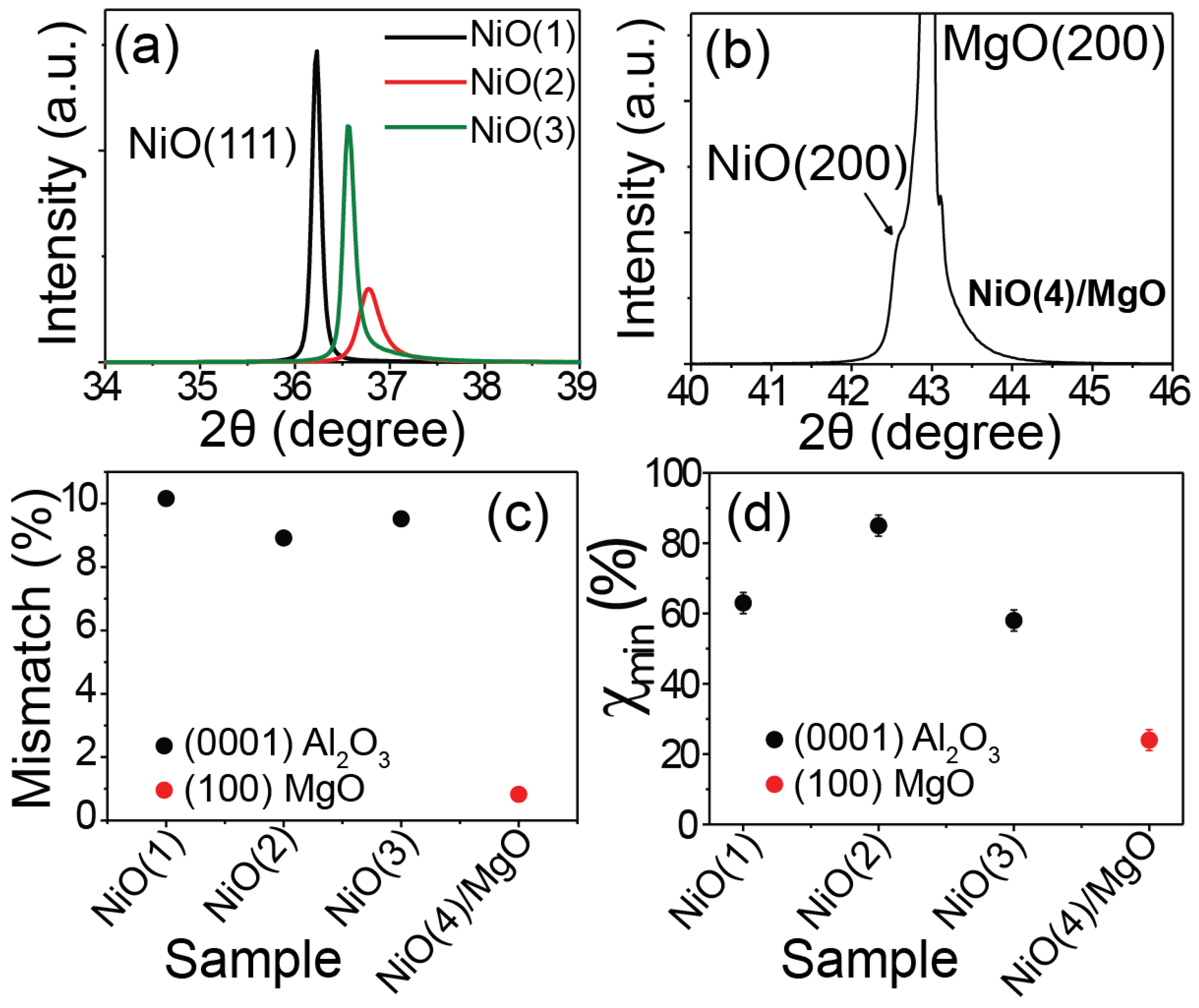
2.1. Film Growth, XRD, and RBS Characterization

NiO thin films can be grown epitaxially on oxide single-crystal substrates. (100) NiO epitaxial films have been usually grown on (100) MgO substrates, while (111) MgO and c-cut Al 2 O 3 substrates have been used to obtain epitaxial (111) NiO films. In this last case, a biepitaxial growth with both in-plane relationships, including [ 1 ¯ 1 ¯ 0 ] NiO// [ 00 1 ¯ 0 ] Al 2 O 3 and [ 1 ¯ 1 2 ¯ ] NiO// [ 2 1 ¯ 1 ¯ 0 ] Al 2 O 3 , has been reported [39,40]. In this work, NiO thin films were deposited on (0001) Al 2 O 3 and (100) MgO substrates by ion beam sputtering using Ar + ions from a 3 cm Kaufmann-type ion source of a pure nickel ( 99.99 % ) target in a controlled atmosphere of oxygen and argon. The NiO thin films were deposited in a vacuum chamber with a base pressure of 2 × 10 5 Pa. During the deposition, the pressure was maintained between 1.8 × 10 2 and 4.1 × 10 2 Pa, and the substrates were rotated at 2 rpm to increase the homogeneity of the deposit. The substrate temperature during deposition, the oxygen partial pressure, and the sputtering conditions (i.e., current density of sputtered Ni atoms, J s p , and energy of the sputtering Ar + ions, E s p ), are shown in Table 1.
The crystal structure and texture of the different films deposited on (0001) Al 2 O 3 and (100) MgO substrates were analyzed with X-ray diffraction (XRD) in a θ / 2 θ configuration using a PANanalytical X’Pert MPD system and Cu-K α radiation. Figure 1a shows the XRD scans corresponding to the NiO (111) peak region for the films grown on (0001) Al 2 O 3 substrates. It should be noted that only the NiO (111), NiO (222) and Al 2 O 3 (006) diffraction peaks can be distinguished in the complete diffractogram (not shown), indicating the epitaxial character of the growth. For the NiO(2) film exclusively, in addition to the NiO (111) peak, a very small NiO (200) peak also appears at ∼43.2 (not shown in the figure), indicating that this film is highly (111) oriented but can have a polycrystalline nature. Figure 1b shows the XRD scan of the NiO film grown on (100) MgO substrate in which a shoulder at ∼42.6 corresponding to the NiO (200) diffraction plane can be distinguished in the intense (200) peak from the MgO substrate. The lattice mismatch between NiO films and (0001) Al 2 O 3 substrate was calculated following the well-known crystallographic orientation relationships and the domain-matching epitaxy proposed by Lee et al. [39] and are plotted in Figure 1c. This figure also includes the lattice mismatch for NiO(4) film grown on (100) MgO substrate following the epitaxial relationship [ 100 ] NiO/ [ 100 ] MgO.
In order to explore the elemental distribution, thickness, and epitaxial quality of the deposited thin films, Rutherford backscattering spectrometry (RBS) was performed under both random and channeling conditions using 4 He + at 1.8 MeV in a 5 MV tandem accelerator [41]. The ion fluence for the Rutherford backscattering was 20 μC. A silicon barrier detector, at a scattering angle of 170 . 5 , measured the backscattering ions while a three-axis goniometer was employed to control the crystal position. The elements present in the thin films and in the substrate were identified in the spectra (not shown here), where the width of each peak corresponded to the relative thickness. The distribution and quantification of the various elements were determined with the SIMNRA simulation software (version 7.02) package. If the material of the film is oriented along the substrate and the direction of the incident 4 He + particles is aligned in the substrate orientation direction, most of the particles will pass through the channel or empty space available within the crystal lattice, leading to a lower yield. The energetic ions can move into the crystals, penetrating much deeper if the atoms in the crystal are directed in some specific crystal directions. The decrease of the yield when the film is aligned is an indication of the epitaxial character of the films. Figure 1d shows the minimum yield ratio between channeling and random spectra for the different NiO films. The lowest value is found in the NiO(4)/MgO film, which is in good agreement with the lowest mismatch found in this film as can be observed in Figure 1c.

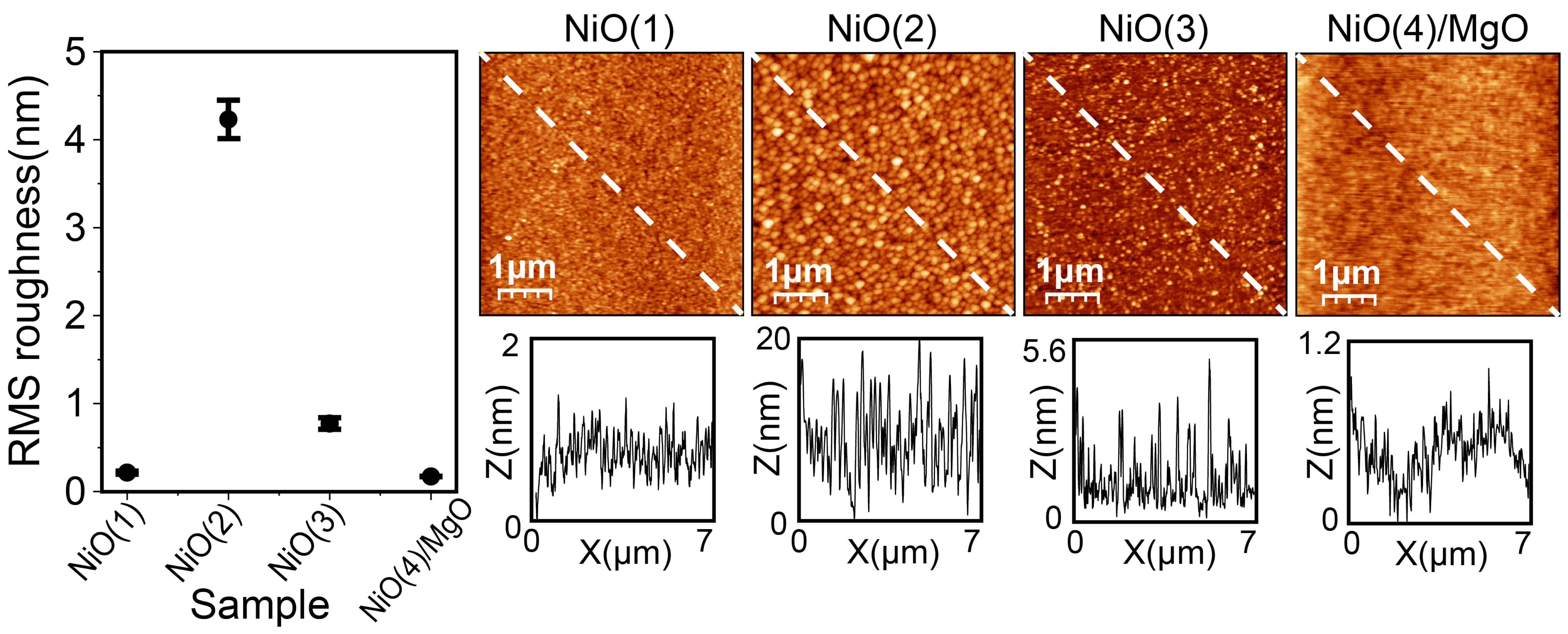
2.2. Atomic Force Microscopy Characterization

Atomic force microscopy measurements were carried out on different virgin NiO films (see Figure 2) using an instrument from Nanotec Electronica S.L. controlled with the WSxM software (version 5.0) [42]. Both typical images and root-mean-square (RMS) roughness analysis were in general agreement with XRD and RBS characterization, pointing toward the most flat surface in NiO(4)/MgO and the greatest roughness in NiO(2) film.

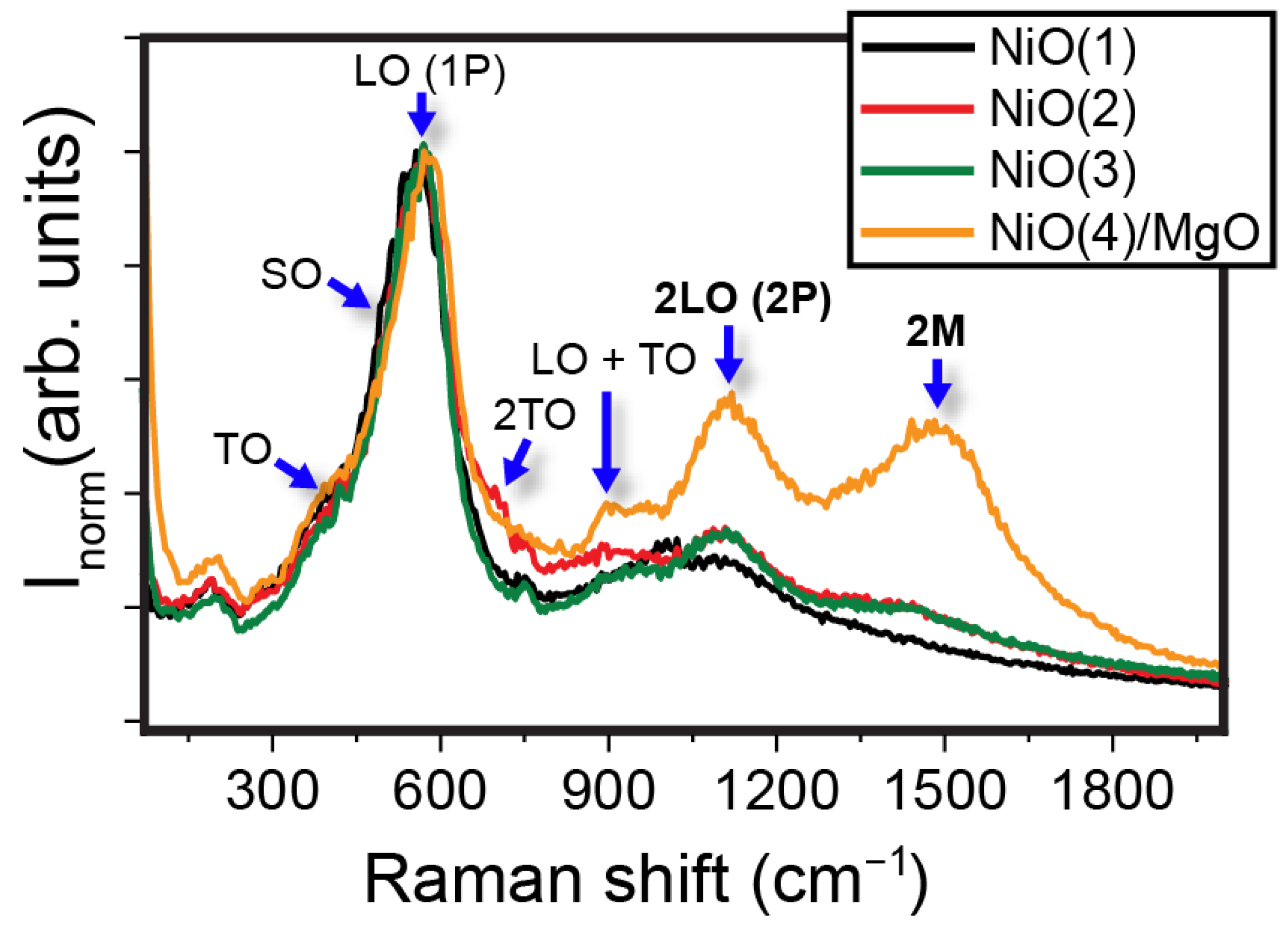
2.3. Micro-Raman Characterization

Confocal micro-Raman experiments were conducted on as-grown NiO films and on the same films immediately after microwave exposure. The measurements were collected using a WITec ALPHA 300RA confocal Raman microscope (CRM) at room temperature with a Nd:YAG linearly polarized laser (532 nm). The Raman spectra were recorded in the range of 0–3600 cm 1 using an objective with a numerical aperture of 0.95 and a laser excitation power of 3.2 mW to avoid any damage to the films. The NiO films were investigated on the plane (XY scans) and in-depth (XZ scans) regions. The collected spectra were analyzed with WITec Project Plus software (version 2.08).
NiO is widely studied with Raman spectroscopy due to its room-temperature AFM behavior. Raman spectra recorded from different NiO films deposited on (0001) Al 2 O 3 and MgO (100) substrates are shown in Figure 3. The Raman signal was collected from the confocal plane of the film with the highest intensity, and thus several Raman spectra from different regions were averaged. Complementarily, a Raman study was performed in both types of substrates in order to discriminate their specific Raman signal. The Raman signal related to the Al 2 O 3 substrate could be identified around 420 and 754 cm 1 on the NiO films (see Appendix A). The MgO substrate did not show Raman modes but rather a fluorescence signal at higher wave numbers (from 2700 cm 1 ) that did not interfere with the active modes of NiO.
The active Raman modes were in full agreement with those of previous reports [43,44], confirming the generally good quality of the NiO films. The first-order phonon modes, longitudinal optical (LO), 1P and transverse optical (TO) are inactive Raman modes in the perfect rock salt-like structure and can appear due to the rhombohedral lattice distortion and the presence of impurity atoms in the crystal lattice. Their intensity is strongly dependent on the stoichiometric ratio in the lattice. The surface optical (SO) phonon mode was also marked in the Raman spectra and represents a well-known indicator for identifying surface defects and roughness [44]. This band was practically imperceptible due to the good quality and low roughness of the films, confirmed by the XRD and atomic force microscopy results. At higher wave numbers, the 2TO, LO + TO, and the 2LO(2P) overtones were identified, as well as the two-magnon mode (2M). The 2LO (2P) Raman mode at 1120 cm 1 can be attributed to biaxial strain in NiO films, and the quotient I 1 P ( L O ) /I 2 P ( 2 L O ) can be considered an inverse figure of merit providing information about the crystal quality of the films [45]. The lowest intensity quotient was measured for NiO(4)/MgO and the largest one for NiO(1) (see Figure 3). Finally, the 2M band (two-magnon mode) at about 1500 cm 1 was measurable as a fingerprint of AFM ordering, identifying the largest intensity for NiO(4)/MgO and the lowest one for NiO(1). Additionally, a redshift was observed along with an intensity decrease of the 2M mode, which can be explained by a reduction in the AFM coupling via Ni-O super exchange interaction [46].

2.4. Magnetic Force Microscopy Characterization

All the measurements were performed at ambient conditions using a scanning force microscope from Nanotec Electronica S.L. controlled with WSxM software (version Develop 8.1) [42]. Commercial MFM probes from Nanosensors PPP-MFMR and Budget Sensors (MultiM-75) were used. The magnetic probes were always calibrated before and after each experiments to verify their performance, especially when no MFM signal was detected. Amplitude modulation method was carried out to enable the phase-locked loop (PLL) to track the resonance frequency of the oscillating cantilever, and the magnetic signal was therefore recorded in the frequency shift channel in Hz. In addition, the acquisition of electrostatic force microscopy images was completed with a PtIr metallic tip from Nanosensors.

3. Results

In order to present the main findings related to the influence of the microwave response on magnetic textures in initially virgin NiO films, we mainly concentrate on the description of the data obtained on the NiO(3) and NiO(4)/MgO films, for which detailed MFM imaging was carried out.

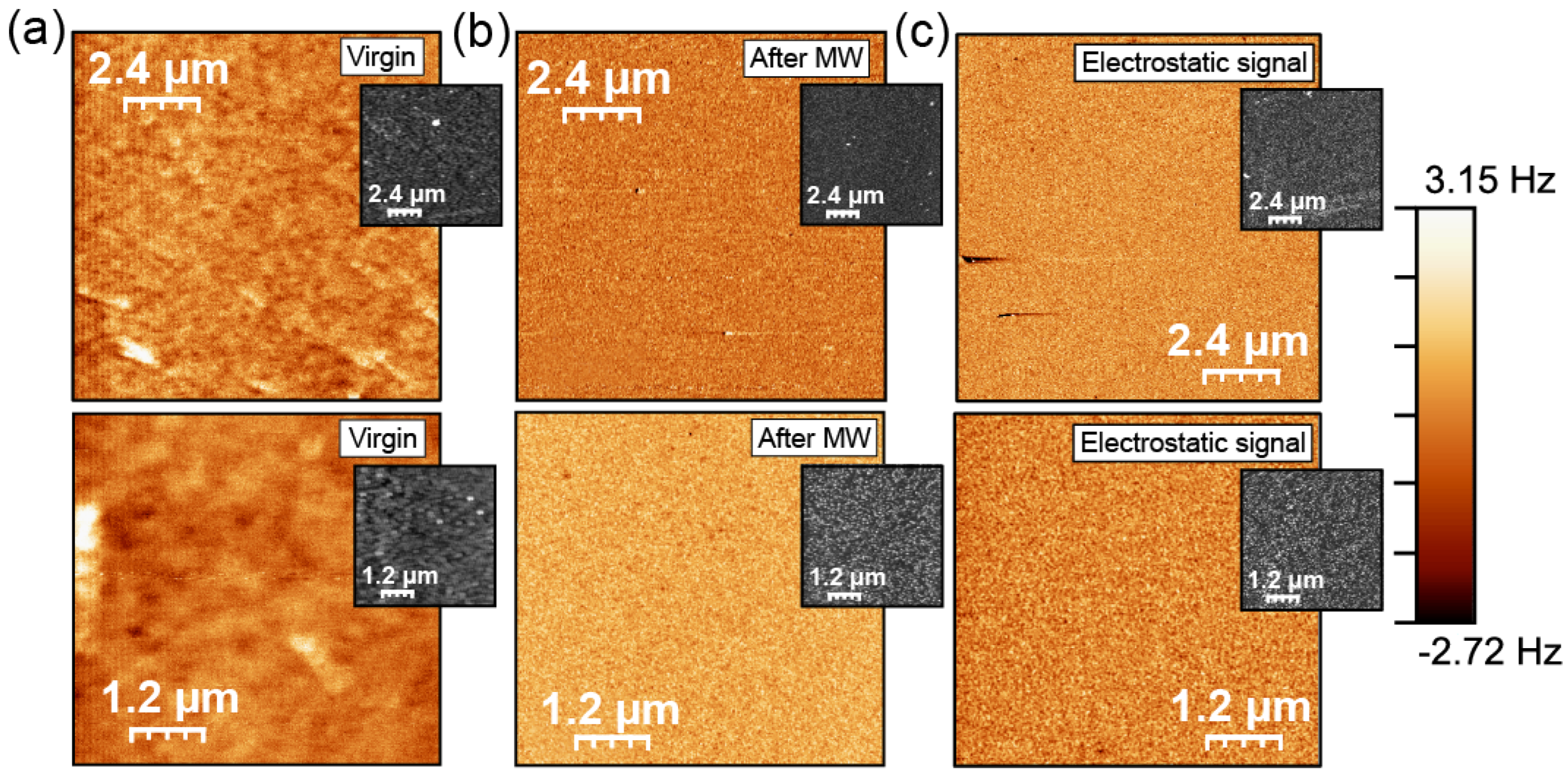
3.1. Influence of MWs on MFM Images in Virgin NiO Films

MFM is one of the most powerful tools for investigating magnetic materials at the nanoscale [47]. However, imaging AFM domains or domain walls with this technique remains challenging. Nitrogen vacancy (NV) magnetometry [5], spin-polarized STM [48], or the combination of MFM with magnetic exchange force microscopy [49] are some of the emerging imaging methods for studying AFM order. Nonetheless, MFM has been used to investigate the influence of crystallographic defects in AFM materials such as NiO [50].
We correlated our results with MFM images and confocal Raman spectroscopy in order to verify if the microwave excitations affected the magnetic textures. Two types of experiments were carried out along this line. First, we investigated both MFM and micro-Raman on the virgin samples, which had not yet been exposed to the application of any microwave drive. Then, the same measurements were performed immediately after (less than 1 h) the application of the maximum available microwave excitation of 5 dBm.
Within the resolution of our MFM setup, magnetic textures were invisible in the virgin NiO(4)/MgO films, probably due to too-low values of the stray fields from AFM DWs in the most perfect NiO films.
On the other hand, MFM imaging on NiO(3) (see Figure 4a) can reveal the presence of irregular magnetic textures similar to those typically observed in synthetic [51] or natural Ni antiferromagnets [23]. Separate checks using Kelvin probe force microscopy [52] with electrostatic tip have proven that MFM images are related to magnetic and not electrostatic interactions as could potentially happen when imaging weakly magnetic insulators.
We also investigated MFM images on the same NiO(3) film two weeks after the maximum microwave drive was last applied. Our measurements could not detect any large-scale magnetic textures but did reveal a much more localized response that was probably related to the dislocation-induced weak ferromagnetism that has been previously reported in NiO [50].

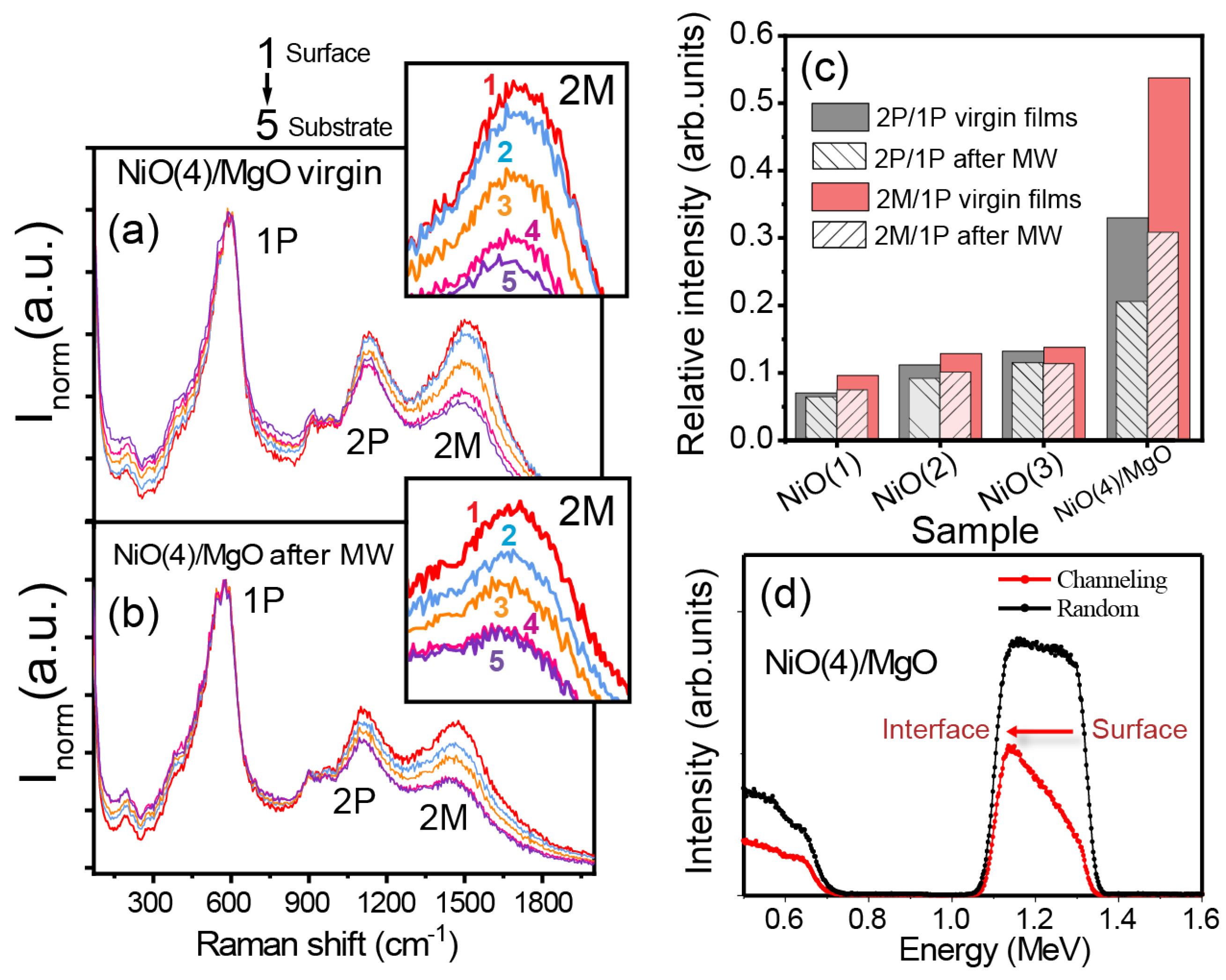
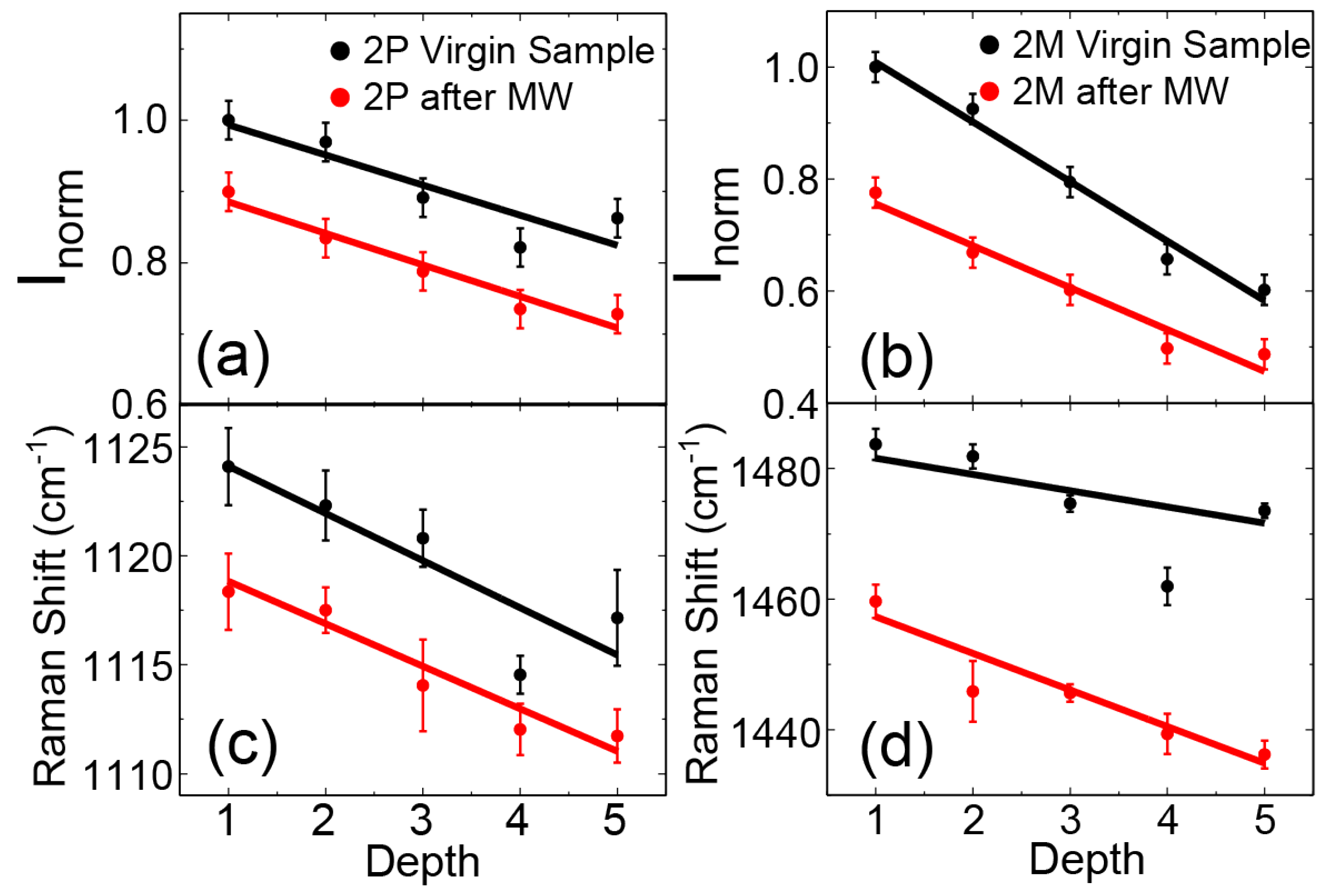
3.2. Influence of Microwaves on Raman Modes in Virgin NiO Films

In order to further explore a possible correlation between magnetic textures and the irradiated MWs, we carried out confocal micro-Raman experiments.
The typical Raman signal for NiO was collected [43,44], with the Raman modes differing depending on the film. As shown in Figure 5, the effect of the MW application on the Raman spectra was recorded, and an in-depth analysis of the films was also carried out. Figure 5a,b and Figure 6a–d show, in the example of NiO(4)/MgO, how the Raman modes changed with the film depth. This could be related to a structural variation from the interface with the substrate toward the film surface, which was confirmed by the channeling characterization (see Figure 5d): there is an agreement between the yield ratio of aligned to random spectra, which increases from the surface to the interface, and the intensity of the 2M Raman mode. Figure 5c shows the analysis of the relative intensity of the 2P and 2M overtones with respect to the 1P band for all the films investigated and demonstrates their variation within in few hours following the application of a 5 dBm microwave field. The variation was especially pronounced for the NiO(4)/MgO sample. Based on the observed MFM reduction of large scale AFM DWs, we propose that this reduction of the amplitude of the Raman active modes is related to AFM magnons (2M mode) and reflects structural imperfections (the intensity relation between 1P and 2P bands is proportional to the degree of structural order) [45,46], which could be linked to the magnetostrictive character of AFM DWs in NiO [23]. As a consequence, once the microwave drive has perturbed the complex AFM DW order, the system tends to recover its complexity by moving and creating large-scale AFM DWs and moving back toward the energy minimum during the Raman experiments. Such slow AFM DW dynamics and rearrangements (which could take place in a timescale of weeks) and related lattice distortions may be responsible for the relative suppression of the 2P and 2M Raman modes in the NiO films previously excited by the microwaves.

4. Discussion and Conclusions

Let us discuss a possible mechanism behind the absorption of the GHz range microwaves by the AFM NiO films with magnons in the THz range. Following Ref. [37], we consider the existence of low-frequency excitations in NiO localized within the magnetic textures (AFM DWs). Indeed, the dispersion relation for the soft branch is predicted to be gapless due to string-like domain wall excitation in AFMs. These localized modes should be similar to Winter magnons [53,54] excited along domain walls in ferromagnets. Similar types of SW excitations along antiferromagnetic DWs have been predicted in Ref. [55]. Numerical calculations [55] show that fast and long-wavelength SWs could propagate distances of 100–1000 nm within tens of picoseconds. In our study, we deduced propagation SW distances from a comparison of the structural (Figure 2) and MFM images (Figure 4), indicating a dislocation density of about one for each 100 nm and an average pinning length of the DWs in a range of 100–1000 nm. The corresponding timescales are therefore close to the relevant frequency of 16 GHz reported experimentally (see Appendix C). However, further studies are needed to verify this scenario.
A high-power microwave excitation may lead to irreversible changes in the magnetic texture of the NiO films via localized heating of the DWs. Such a scenario is suggested by the difference in the Raman and MFM responses seen on the samples before and after a high-power MW excitation was applied. We therefore relate these irreversible changes in magnetic textures to the localized power absorption of spin waves confined around the AFM domain walls/textures [37].
As long as the sample face excited by MWs is in contact with the coplanar waveguide (CWG), it is impossible to measure the temperature of the NiO surface in our setup and thus to directly evaluate the local heating of DWs. Therefore, the temperature measurements were conducted on the backside of the NiO(4)/MgO sample with an infrared (IR) camera. We note that the temperature variation of the substrate side during the application of MW powered up to + 5 dBm did not exceed ∼1 K.
This upper limit is in agreement with numerical simulations made with COMSOL (Appendix B) and with simple analytical estimations based on the maximum power dissipated by the MWs into the NiO sample. Therefore, we did rule out the possibility that, in addition to the direct excitation of DWs (magnetic textures) by the MWs, there could be a localized heating close to those textures where the MW losses should be enhanced. This additional local heating (which is hardly detectable with the IR camera or the COMSOL simulations) could help the system to thermally overcome the energy barrier between its textured state and the global minimum energy state with a more spatially homogeneous magnetic order. This effect, in combination with the direct excitation of AFM-DWs by the MWs, could be the underlying cause of the observed reduction of DWs after exposure to the microwave excitation.
Finally, we point out that microwave permeability experiments as a function of MW power carried out on a virgin NiO film (see Appendix C) showed a resonant response between 15 and 17 GHz, with an increasing magnitude and a frequency shift once the MW power exceeded 15 dBm. Similar measurements carried out on the substrate (MgO) side of the sample showed a background nearly independent of the MW power. We believe that this kind of MW-induced excitation could account for the above-described changes in Raman modes and MFM images of the AFM NiO films.

Author Contributions

Conceptualization F.G.A. and P.P.; methodology, A.S., D.C., M.J., F.G.A. and P.P.; software, D.C. and C.G.-R.; validation, A.S., F.G.A., D.C. and C.G.-R.; formal analysis, A.S., M.J., D.C. and P.P.; investigation, D.C., C.G.-R., P.P., A.K. and F.G.A.; resources, F.G.A. and P.P.; data curation, M.J., A.S. and D.C.; writing—original draft preparation, F.G.A., D.C., P.P., A.S., M.J. and A.K.; writing—review and editing, F.G.A., D.C., C.G.-R. and A.K.; visualization, D.C. and C.G.-R.; supervision, F.G.A.; project administration, F.G.A. and P.P.; funding acquisition, F.G.A. and P.P. All authors have read and agreed to the published version of the manuscript.

Funding

This research was funded by the Spanish Ministerio de Ciencia e Innovación (PID2021-124585NB-C32, PID2021-124585NB-C33, PID2021-122980OA-C53, and TED2021-130196B-C22). F.G.A. also acknowledges financial support from the Spanish Ministerio de Ciencia e Innovación through the María de Maeztu Programme for Units of Excellence in R&D (CEX2018-000805-M) and “Acción financiada por la Comunidad de Madrid en el marco del convenio plurianual con la Universidad Autónoma de Madrid en Línea 3: Excelencia para el Profesorado Universitario”. P.P. acknowledges the support of the Comunidad de Madrid and Universidad Autonoma de Madrid under the V PRICIT program through the Project SI3/PJI/2021-00393. A.S. acknowledges the financial support from MICINN for a Ramón y Cajal contract (RYC2021-031236-I), which was funded by the Recovery, Transformation and Resilience Plan.

Institutional Review Board Statement

Not applicable.

Informed Consent Statement

Not applicable.

Data Availability Statement

Data will be made available upon reasonable request.

Conflicts of Interest

The authors declare no conflicts of interest.

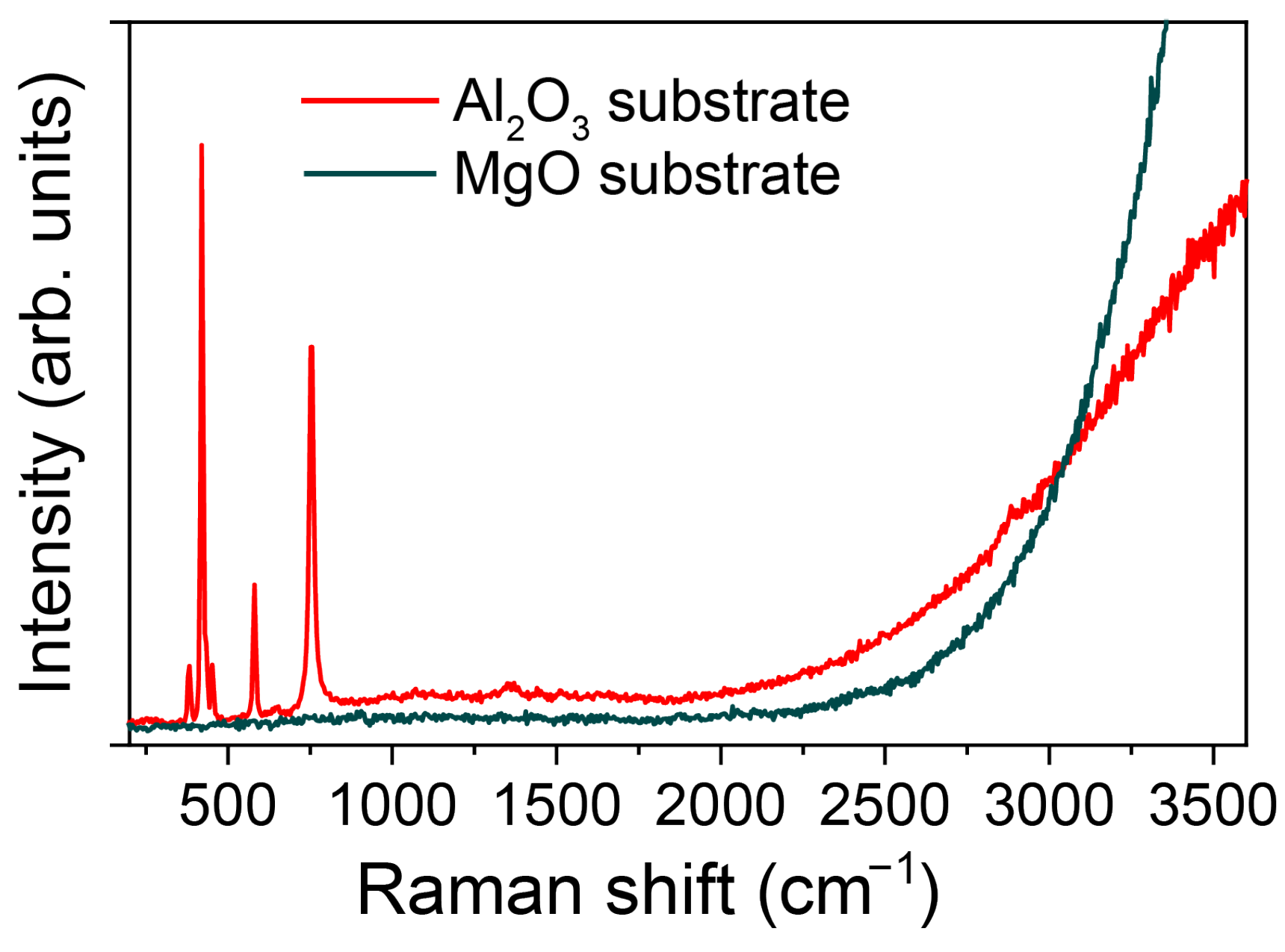
Appendix A. Control Raman Experiments on the MgO and Al2O3 Substrates

Raman spectroscopy was conducted on the used substrates. In the case of the MgO, only a fluorescence signal above 2700 cm 1 was detected but no Raman band. The Al 2 O 3 substrate presented several Raman modes, with the highest intensity for those located around 420 and 754 cm 1 , which was observed in the Raman signal measured in the samples with this specific substrate.
Figure A1. Raman signal of the MgO and Al 2 O 3 substrates used in our NiO samples.
Condensedmatter 09 00007 g0a1
Figure A2. COMSOL simulations of the temperature difference between the NiO(4)/MgO and the room temperature for different irradiated MW powers. Curves for upper ( ϵ = 0.6 ) and lower ( ϵ = 0.2 ) surface emissivity bounds are presented.
Condensedmatter 09 00007 g0a2

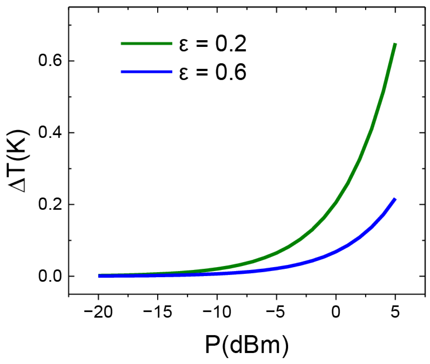
Appendix B. COMSOL Simulations on the Temperature Provided by the MW Heating on the Sample

COMSOL simulations were conducted to obtain the temperature increase on the NiO(4)/MgO sample when exposed to MW radiation. It is important to notice that these simulations are limited by the possible magnetic textures in the sample, which are not replicated. To emulate the MW irradiation, we implemented a homogeneous heat source on the NiO side of the sample. On the other boundaries, we allowed surface-to-ambient radiation ( T a m b i e n t = 300 K).
We observed that the maximum temperature increase did not exceed 0.7 K in the lower surface emissivity bound or 0.3 K in the upper bound, as seen in Figure A2. This is in agreement with our previous temperature estimations. However, it is important to acknowledge that localized heating within the magnetic textures cannot be ruled out, as previously suggested.

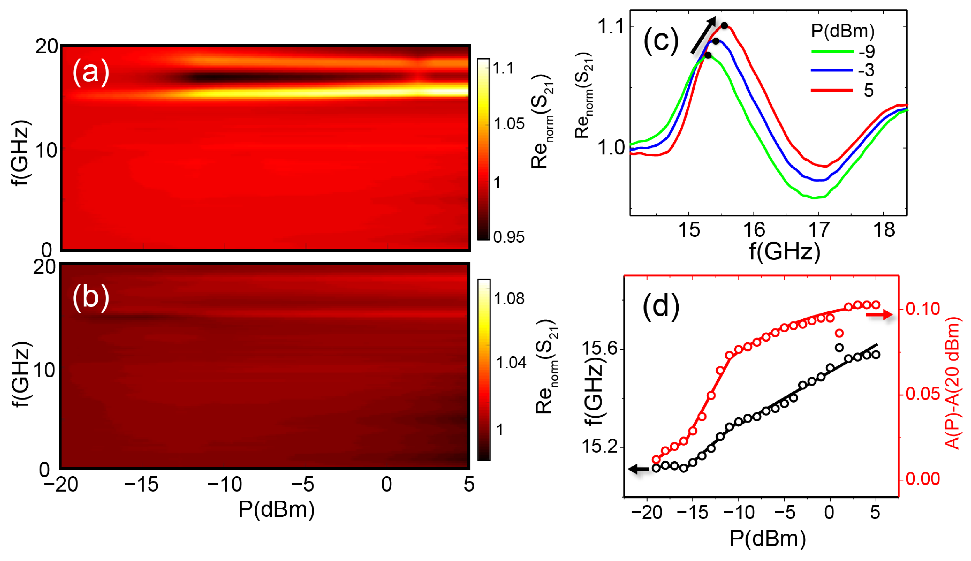
Appendix C. Microwave Transmission Measurements as a Function of Power

Figure A3. Real part of the scattering matrix element S 21 normalized to 20 dBm as measured for the NiO(4)/MgO sample as a function of the MW power. (a) Measurement performed with the NiO side facing the CPW. (b) Measurement performed with the substrate (MgO) facing the CPW. (c) Cross-sections of the peak around 15 GHz seen in part (a) for different MW powers, illustrating its displacement. (d) Frequency and amplitude of the 15–16 GHz peak against the MW power. The peak position was resolved by fitting the peak in the Re n o r m (S 21 ) cross-sections to a Lorentzian curve.
Condensedmatter 09 00007 g0a3
In order to probe the dynamic magnetic response of the different samples, a vector network analyzer (VNA) high-frequency setup was used (see [54] for details), with the films being placed directly on top of a coplanar waveguide (CPW).
In these MW experiments, driving AC fields of up to 5 dBm were applied to the NiO(4)/MgO sample on its virgin state. The microwave frequency covered a frequency range between 10 MHz and 20 GHz. Transmission measurements were made by sweeping this frequency at a zero bias DC field and averaging 20 measurements for each dBm to ensure noise reduction. The scattering matrix element S 21 measured with the VNA, which was the relation between the magnitude and phase of the input signal sent to the CPW and the received signal and indicative of the transmission in the system [56].
To ensure a response related to the antiferromagnetic sample, control measurements were performed on the substrate face and the NiO face of the sample. Figure A3 shows a zero-field measurement of the normalized real part of the S 21 scattering matrix element of the NiO(4)/MgO virgin sample, for a MW power from 20 dBm to 5 dBm. Figure A3a shows the dynamic response of the NiO, with panel b corresponding to the MgO substrate. Panels c,d are the analysis of the peak amplitude and frequency observed in the NiO side as a function of the applied MW power.

References

  1. Satoh, T.; Cho, S.J.; Iida, R.; Shimura, T.; Kuroda, K.; Ueda, H.; Ueda, Y.; Ivanov, B.A.; Nori, F.; Fiebig, M. Spin Oscillations in Antiferromagnetic NiO Triggered by Circularly Polarized Light. Phys. Rev. Lett. 2010, 105, 077402. [Google Scholar] [CrossRef] [PubMed]
  2. Moriyama, T.; Hayashi, K.; Yamada, K.; Shima, M.; Ohya, Y.; Ono, T. Intrinsic and extrinsic antiferromagnetic damping in NiO. Phys. Rev. Mater. 2019, 3, 051402. [Google Scholar] [CrossRef]
  3. Kampfrath, T.; Sell, A.; Klatt, G.; Pashkin, A.; Mährlein, S.; Dekorsy, T.; Wolf, M.; Fiebig, M.; Leitenstorfer, A.; Huber, R. Coherent terahertz control of antiferromagnetic spin waves. Nat. Photonics 2010, 5, 31–34. [Google Scholar] [CrossRef]
  4. Lebrun, R.; Ross, A.; Bender, S.A.; Qaiumzadeh, A.; Baldrati, L.; Cramer, J.; Brataas, A.; Duine, R.A.; Kläui, M. Tunable long-distance spin transport in a crystalline antiferromagnetic iron oxide. Nature 2018, 561, 222–225. [Google Scholar] [CrossRef] [PubMed]
  5. Hedrich, N.; Wagner, K.; Pylypovskyi, O.V.; Shields, B.J.; Kosub, T.; Sheka, D.D.; Makarov, D.; Maletinsky, P. Nanoscale mechanics of antiferromagnetic domain walls. Nat. Phys. 2021, 17, 574–577. [Google Scholar] [CrossRef]
  6. Ross, A.; Lebrun, R.; Gomonay, O.; Grave, D.A.; Kay, A.; Baldrati, L.; Becker, S.; Qaiumzadeh, A.; Ulloa, C.; Jakob, G.; et al. Propagation Length of Antiferromagnetic Magnons Governed by Domain Configurations. Nano Lett. 2019, 20, 306–313. [Google Scholar] [CrossRef]
  7. Song, C.; You, Y.; Chen, X.; Zhou, X.; Wang, Y.; Pan, F. How to manipulate magnetic states of antiferromagnets. Nanotechnology 2018, 29, 112001. [Google Scholar] [CrossRef]
  8. Kim, S.K.; Tchernyshyov, O.; Tserkovnyak, Y. Thermophoresis of an antiferromagnetic soliton. Phys. Rev. B 2015, 92, 020402. [Google Scholar] [CrossRef]
  9. Zhang, Y.L.; Chen, Z.Y.; Yan, Z.R.; Chen, D.Y.; Fan, Z.; Qin, M.H. Staggered field driven domain walls motion in antiferromagnetic heterojunctions. Appl. Phys. Lett. 2018, 113, 112403. [Google Scholar] [CrossRef]
  10. Bodnar, S.Y.; Skourski, Y.; Gomonay, O.; Sinova, J.; Kläui, M.; Jourdan, M. Magnetoresistance Effects in the Metallic Antiferromagnet Mn2Au. Phys. Rev. Appl. 2020, 14, 014004. [Google Scholar] [CrossRef]
  11. Yu, W.; Lan, J.; Xiao, J. Polarization-selective spin wave driven domain-wall motion in antiferromagnets. Phys. Rev. B 2018, 98, 144422. [Google Scholar] [CrossRef]
  12. Qaiumzadeh, A.; Kristiansen, L.A.; Brataas, A. Controlling chiral domain walls in antiferromagnets using spin-wave helicity. Phys. Rev. B 2018, 97, 020402. [Google Scholar] [CrossRef]
  13. Gomonay, O.; Jungwirth, T.; Sinova, J. High Antiferromagnetic Domain Wall Velocity Induced by Néel Spin-Orbit Torques. Phys. Rev. Lett. 2016, 117, 017202. [Google Scholar] [CrossRef]
  14. Wadley, P.; Howells, B.; Železný, J.; Andrews, C.; Hills, V.; Campion, R.P.; Novák, V.; Olejník, K.; Maccherozzi, F.; Dhesi, S.S.; et al. Electrical switching of an antiferromagnet. Science 2016, 351, 587–590. [Google Scholar] [CrossRef] [PubMed]
  15. Meer, H.; Schreiber, F.; Schmitt, C.; Ramos, R.; Saitoh, E.; Gomonay, O.; Sinova, J.; Baldrati, L.; Kläui, M. Direct Imaging of Current-Induced Antiferromagnetic Switching Revealing a Pure Thermomagnetoelastic Switching Mechanism in NiO. Nano Lett. 2020, 21, 114–119. [Google Scholar] [CrossRef]
  16. Churikova, A.; Bono, D.; Neltner, B.; Wittmann, A.; Scipioni, L.; Shepard, A.; Newhouse-Illige, T.; Greer, J.; Beach, G.S.D. Non-magnetic origin of spin Hall magnetoresistance-like signals in Pt films and epitaxial NiO/Pt bilayers. Appl. Phys. Lett. 2020, 116, 022410. [Google Scholar] [CrossRef]
  17. Keffer, F.; Kittel, C. Theory of Antiferromagnetic Resonance. Phys. Rev. 1952, 85, 329–337. [Google Scholar] [CrossRef]
  18. Safin, A.R.; Nikitov, S.A.; Kirilyuk, A.I.; Kalyabin, D.V.; Sadovnikov, A.V.; Stremoukhov, P.A.; Logunov, M.V.; Popov, P.A. Excitation of Terahertz Magnons in Antiferromagnetic Nanostructures: Theory and Experiment. J. Exp. Theor. Phys. 2020, 131, 71–82. [Google Scholar] [CrossRef]
  19. Wang, Z.; Kovalev, S.; Awari, N.; Chen, M.; Germanskiy, S.; Green, B.; Deinert, J.C.; Kampfrath, T.; Milano, J.; Gensch, M. Magnetic field dependence of antiferromagnetic resonance in NiO. Appl. Phys. Lett. 2018, 112, 252404. [Google Scholar] [CrossRef]
  20. Olejník, K.; Seifert, T.; Kašpar, Z.; Novák, V.; Wadley, P.; Campion, R.P.; Baumgartner, M.; Gambardella, P.; Němec, P.; Wunderlich, J.; et al. Terahertz electrical writing speed in an antiferromagnetic memory. Sci. Adv. 2018, 4, eaar3566. [Google Scholar] [CrossRef]
  21. Chirac, T.; Chauleau, J.Y.; Thibaudeau, P.; Gomonay, O.; Viret, M. Ultrafast antiferromagnetic switching in NiO induced by spin transfer torques. Phys. Rev. B 2020, 102, 134415. [Google Scholar] [CrossRef]
  22. Arai, K.; Okuda, T.; Tanaka, A.; Kotsugi, M.; Fukumoto, K.; Ohkochi, T.; Nakamura, T.; Matsushita, T.; Muro, T.; Oura, M.; et al. Three-dimensional spin orientation in antiferromagnetic domain walls of NiO studied by x-ray magnetic linear dichroism photoemission electron microscopy. Phys. Rev. B 2012, 85, 104418. [Google Scholar] [CrossRef]
  23. Weber, N.B.; Ohldag, H.; Gomonaj, H.; Hillebrecht, F.U. Magnetostrictive Domain Walls in Antiferromagnetic NiO. Phys. Rev. Lett. 2003, 91, 237205. [Google Scholar] [CrossRef] [PubMed]
  24. Sänger, I.; Pavlov, V.V.; Bayer, M.; Fiebig, M. Distribution of antiferromagnetic spin and twin domains in NiO. Phys. Rev. B 2006, 74, 144401. [Google Scholar] [CrossRef]
  25. Hortensius, J.R.; Afanasiev, D.; Matthiesen, M.; Leenders, R.; Citro, R.; Kimel, A.V.; Mikhaylovskiy, R.V.; Ivanov, B.A.; Caviglia, A.D. Coherent spin-wave transport in an antiferromagnet. Nat. Phys. 2021, 17, 1001–1006. [Google Scholar] [CrossRef]
  26. Qiu, Z.; Li, J.; Hou, D.; Arenholz, E.; N’Diaye, A.T.; Tan, A.; ichi Uchida, K.; Sato, K.; Okamoto, S.; Tserkovnyak, Y.; et al. Spin-current probe for phase transition in an insulator. Nat. Commun. 2016, 7, 12670. [Google Scholar] [CrossRef]
  27. Dabrowski, M.; Nakano, T.; Burn, D.M.; Frisk, A.; Newman, D.G.; Klewe, C.; Li, Q.; Yang, M.; Shafer, P.; Arenholz, E.; et al. Coherent Transfer of Spin Angular Momentum by Evanescent Spin Waves within Antiferromagnetic NiO. Phys. Rev. Lett. 2020, 124, 217201. [Google Scholar] [CrossRef] [PubMed]
  28. Hahn, C.; de Loubens, G.; Naletov, V.V.; Youssef, J.B.; Klein, O.; Viret, M. Conduction of spin currents through insulating antiferromagnetic oxides. EPL (Europhys. Lett.) 2014, 108, 57005. [Google Scholar] [CrossRef]
  29. Wang, H.; Du, C.; Hammel, P.C.; Yang, F. Antiferromagnonic Spin Transport from Y3Fe5O12 into NiO. Phys. Rev. Lett. 2014, 113, 097202. [Google Scholar] [CrossRef]
  30. Wang, H.; Du, C.; Hammel, P.C.; Yang, F. Spin transport in antiferromagnetic insulators mediated by magnetic correlations. Phys. Rev. B 2015, 91, 220410. [Google Scholar] [CrossRef]
  31. Moriyama, T.; Takei, S.; Nagata, M.; Yoshimura, Y.; Matsuzaki, N.; Terashima, T.; Tserkovnyak, Y.; Ono, T. Anti-damping spin transfer torque through epitaxial nickel oxide. Appl. Phys. Lett. 2015, 106, 162406. [Google Scholar] [CrossRef]
  32. Kimel, A.V.; Ivanov, B.A.; Pisarev, R.V.; Usachev, P.A.; Kirilyuk, A.; Rasing, T. Inertia-driven spin switching in antiferromagnets. Nat. Phys. 2009, 5, 727–731. [Google Scholar] [CrossRef]
  33. Gerasimchuk, V.S.; Gorobets, Y.I.; Goujon-Durand, S. Domain-wall motion in antiferromagnets in microwave fields. Phys. Rev. B 1994, 49, 9608–9612. [Google Scholar] [CrossRef]
  34. Chen, Z.Y.; Yan, Z.R.; Zhang, Y.L.; Qin, M.H.; Fan, Z.; Lu, X.B.; Gao, X.S.; Liu, J.M. Microwave fields driven domain wall motions in antiferromagnetic nanowires. New J. Phys. 2018, 20, 063003. [Google Scholar] [CrossRef]
  35. Han, J.; Zhang, P.; Bi, Z.; Fan, Y.; Safi, T.S.; Xiang, J.; Finley, J.; Fu, L.; Cheng, R.; Liu, L. Birefringence-like spin transport via linearly polarized antiferromagnetic magnons. Nat. Nanotechnol. 2020, 15, 563–568. [Google Scholar] [CrossRef]
  36. Wimmer, T.; Kamra, A.; Gückelhorn, J.; Opel, M.; Geprägs, S.; Gross, R.; Huebl, H.; Althammer, M. Observation of Antiferromagnetic Magnon Pseudospin Dynamics and the Hanle Effect. Phys. Rev. Lett. 2020, 125, 247204. [Google Scholar] [CrossRef]
  37. Flebus, B.; Ochoa, H.; Upadhyaya, P.; Tserkovnyak, Y. Proposal for dynamic imaging of antiferromagnetic domain wall via quantum-impurity relaxometry. Phys. Rev. B 2018, 98, 180409. [Google Scholar] [CrossRef]
  38. Meer, H.; Wust, S.; Schmitt, C.; Herrgen, P.; Fuhrmann, F.; Hirtle, S.; Bednarz, B.; Rajan, A.; Ramos, R.; Niño, M.A.; et al. Laser-Induced Creation of Antiferromagnetic 180-Degree Domains in NiO/Pt Bilayers. Adv. Funct. Mater. 2023, 33, 2213536. [Google Scholar] [CrossRef]
  39. Lee, J.H.; Kwon, Y.H.; Kong, B.H.; Lee, J.Y.; Cho, H.K. Biepitaxial Growth of High-Quality Semiconducting NiO Thin Films on (0001) Al2O3 Substrates: Microstructural Characterization and Electrical Properties. Cryst. Growth Des. 2012, 12, 2495–2500. [Google Scholar] [CrossRef]
  40. Becker, M.; Polity, A.; Klar, P.J. NiO films on sapphire as potential antiferromagnetic pinning layers. J. Appl. Phys. 2017, 122, 175303. [Google Scholar] [CrossRef]
  41. Redondo-Cubero, A.; Borge, M.J.G.; Gordillo, N.; Gutiérrez, P.C.; Olivares, J.; Casero, R.P.; Ynsa, M.D. Current status and future developments of the ion beam facility at the centre of micro-analysis of materials in Madrid. Eur. Phys. J. Plus 2021, 136, 175. [Google Scholar] [CrossRef]
  42. Horcas, I.; Fernández, R.; Gómez-Rodríguez, J.M.; Colchero, J.; Gómez-Herrero, J.; Baro, A.M. WSXM: A software for scanning probe microscopy and a tool for nanotechnology. Rev. Sci. Instrum. 2007, 78, 013705. [Google Scholar] [CrossRef] [PubMed]
  43. Aytan, E.; Debnath, B.; Kargar, F.; Barlas, Y.; Lacerda, M.M.; Li, J.X.; Lake, R.K.; Shi, J.; Balandin, A.A. Spin-phonon coupling in antiferromagnetic nickel oxide. Appl. Phys. Lett. 2017, 111, 252402. [Google Scholar] [CrossRef]
  44. Sunny, A.; Balasubramanian, K. Raman Spectral Probe on Size-Dependent Surface Optical Phonon Modes and Magnon Properties of NiO Nanoparticles. J. Phys. Chem. C 2020, 124, 12636–12644. [Google Scholar] [CrossRef]
  45. Budde, M.; Tschammer, C.; Franz, P.; Feldl, J.; Ramsteiner, M.; Goldhahn, R.; Feneberg, M.; Barsan, N.; Oprea, A.; Bierwagen, O. Structural, optical, and electrical properties of unintentionally doped NiO layers grown on MgO by plasma-assisted molecular beam epitaxy. J. Appl. Phys. 2018, 123, 195301. [Google Scholar] [CrossRef]
  46. Feldl, J.; Budde, M.; Tschammer, C.; Bierwagen, O.; Ramsteiner, M. Magnetic characteristics of epitaxial NiO films studied by Raman spectroscopy. J. Appl. Phys. 2020, 127, 235105. [Google Scholar] [CrossRef]
  47. Kazakova, O.; Puttock, R.; Barton, C.; Corte-León, H.; Jaafar, M.; Neu, V.; Asenjo, A. Frontiers of magnetic force microscopy. J. Appl. Phys. 2019, 125, 060901. [Google Scholar] [CrossRef]
  48. Bode, M.; Vedmedenko, E.Y.; von Bergmann, K.; Kubetzka, A.; Ferriani, P.; Heinze, S.; Wiesendanger, R. Atomic spin structure of antiferromagnetic domain walls. Nat. Mater. 2006, 5, 477–481. [Google Scholar] [CrossRef]
  49. Geng, Y.; Das, H.; Wysocki, A.L.; Wang, X.; Cheong, S.W.; Mostovoy, M.; Fennie, C.J.; Wu, W. Direct visualization of magnetoelectric domains. Nat. Mater. 2013, 13, 163–167. [Google Scholar] [CrossRef]
  50. Sugiyama, I.; Shibata, N.; Wang, Z.; Kobayashi, S.; Yamamoto, T.; Ikuhara, Y. Ferromagnetic dislocations in antiferromagnetic NiO. Nat. Nanotechnol. 2013, 8, 266–270. [Google Scholar] [CrossRef]
  51. Herranz, D.; Guerrero, R.; Villar, R.; Aliev, F.G.; Swaving, A.C.; Duine, R.A.; van Haesendonck, C.; Vavra, I. Anomalous low-frequency noise in synthetic antiferromagnets: Possible evidence of current-induced domain-wall motion. Phys. Rev. B 2009, 79, 134423. [Google Scholar] [CrossRef]
  52. Jaafar, M.; Iglesias-Freire, O.; Serrano-Ramón, L.; Ibarra, M.R.; de Teresa, J.M.; Asenjo, A. Distinguishing magnetic and electrostatic interactions by a Kelvin probe force microscopy–magnetic force microscopy combination. Beilstein J. Nanotechnol. 2011, 2, 552–560. [Google Scholar] [CrossRef] [PubMed]
  53. Winter, J.M. Bloch Wall Excitation. Application to Nuclear Resonance in a Bloch Wall. Phys. Rev. 1961, 124, 452–459. [Google Scholar] [CrossRef]
  54. Aliev, F.G.; Awad, A.A.; Dieleman, D.; Lara, A.; Metlushko, V.; Guslienko, K.Y. Localized domain-wall excitations in patterned magnetic dots probed by broadband ferromagnetic resonance. Phys. Rev. B 2011, 84, 144406. [Google Scholar] [CrossRef]
  55. Park, H.K.; Kim, S.K. Channeling of spin waves in antiferromagnetic domain walls. Phys. Rev. B 2021, 103, 214420. [Google Scholar] [CrossRef]
  56. Müller, M.; Liensberger, L.; Flacke, L.; Huebl, H.; Kamra, A.; Belzig, W.; Gross, R.; Weiler, M.; Althammer, M. Temperature-Dependent Spin Transport and Current-Induced Torques in Superconductor-Ferromagnet Heterostructures. Phys. Rev. Lett. 2021, 126, 087201. [Google Scholar] [CrossRef]
Figure 1. XRD diffraction patterns of (a) (111) NiO films grown on (0001) Al 2 O 3 substrate and (b) (100) NiO film grown on (100) MgO substrate. (c) Lattice mismatch with the substrate and (d) minimum yield ratio obtained from the channeling and random RBS spectra for the NiO films grown on the (0001) Al 2 O 3 and (100) MgO substrates.
Condensedmatter 09 00007 g001
Figure 2. Atomic force microscopy characterization of the NiO films. RMS roughness of the films was measured on several images showing an average value. Error bars constitute the standard deviation of the measurements. The dotted lines represent the scanning region leading to the corresponding captured topographic profiles on each sample. All of the samples were quite flat and free from surface defects, especially NiO(1) and NiO(4)/MgO. NiO(2) demonstrated much greater roughness than did the other samples.
Condensedmatter 09 00007 g002
Figure 3. Resolved Raman modes for all the analyzed NiO films in the virgin state. The active modes are in agreement with those of previous reports [43,44], indicating the good quality of the films. The 2LO (2P) and 2M modes were especially visible in the NiO(4)/MgO sample. The Raman spectra are normalized to the LO mode (1P).
Condensedmatter 09 00007 g003
Figure 4. Two MFM resolved images of different regions (upper and lower panels) of the NiO(3) sample (a) before and (b) after the application of a MW excitation. The magnetic texture observed in the virgin state disappeared after the MW application, in line with our proposed interpretation. (c) shows the electrostatic image, which suggest a purely magnetic nature of the observed features. The black-and-white insets are the topographical map of each region.
Condensedmatter 09 00007 g004
Figure 5. Resolved Raman spectra in the in-depth direction (XZ plane) for the NiO(4)/MgO sample (a) in its virgin state and (b) immediately after being put through a maintained microwave drive of 5 dBm. The normalization of the intensity signal was completed by adjusting the 1P band. The assignation of the 1P, 2P, and 2M active modes is marked on the figure. Raman spectra correspond to equidistant points in the depth profile of the film from the film surface (1) to the substrate interface (5). This analysis shows extraordinary variation of the 2P and 2M modes in the depth coordinate. (c) Relative intensity of 2P/1P and 2M/1P on the virgin films and after the application of MW. There was a correlation between the reduction of the intensity of the 2P and 2M modes and the application of MW for all of the analyzed samples. The NiO(4)/MgO sample was particularly sensitive to the effect of the MW, partially since the 2P and 2M modes were highly manifest. (d) Channeling and random RBS spectra of the NiO(4)/MgO sample.
Condensedmatter 09 00007 g005
Figure 6. Behavior of the 2P (a,c) and 2M (b,d) Raman modes in the NiO(4)/MgO sample against the depth of the analysis before and after a continuous application of a MW field. (a,b) Intensity of the modes normalized by the maximum value before the MW pumping. (c,d) Raman shift of the modes’ peaks.
Condensedmatter 09 00007 g006
Table 1. NiO thin film deposition parameters: substrate temperature, oxygen partial pressure, Ar + energy, and sputter current density. The thickness determined by RBS quantification and the out-of-plane lattice parameter determined by XRD are also included.
NiO(1)NiO(2)NiO(3)NiO(4)/MgO
SubstrateAl 2 O 3 (0001)Al 2 O 3 (0001)Al 2 O 3 (0001)MgO (100)
T substrate (K)633718798798
PO 2 (Pa) 1.3 × 10 2 2.2 × 10 2 2.8 × 10 2 2.8 × 10 2
J sp (mA/cm 2 )1.61.41.11.1
E sp (eV)650650650650
Thickness (nm)244228195207
Deposition rate (A/s)0.330.330.270.26
Lattice parameter (nm)0.4280.4230.4260.425
Disclaimer/Publisher’s Note: The statements, opinions and data contained in all publications are solely those of the individual author(s) and contributor(s) and not of MDPI and/or the editor(s). MDPI and/or the editor(s) disclaim responsibility for any injury to people or property resulting from any ideas, methods, instructions or products referred to in the content.

