Technical Note

Methods to Create Novel La2−xSrxCuO4 Devices with Multiple Atomically Sharp Interfaces

1
Condensed Matter Physics and Materials Science Division, Brookhaven National Laboratory, Upton, NY 11973-5000, USA
2
Department of Chemistry, Yale University, New Haven, CT 06520, USA
3
Energy Sciences Institute, Yale University, West Haven, CT 06516, USA
4
Department of Physics, The University of Texas at Dallas, Richardson, TX 75080-3021, USA
*
Authors to whom correspondence should be addressed.
Condens. Matter 2023, 8(1), 14; https://doi.org/10.3390/condmat8010014
Submission received: 23 December 2022 / Revised: 17 January 2023 / Accepted: 17 January 2023 / Published: 20 January 2023

Abstract

:
We present methods to create devices that utilize the high-temperature superconductor La2-xSrxCuO4 grown by atomic layer-by-layer molecular beam epitaxy (ALL-MBE). The ALL-MBE synthesis technique provides atomically precise interfaces necessary for the tunnel junctions, Josephson junctions, and dyon detection devices that will be considered. A series of microfabrication processing steps using established techniques are given for each device, and their details are discussed. These procedures are easily extended to generate more complex designs and could be suitable for a wider variety of materials.

1. Introduction

The copper oxide materials that superconduct at high critical temperatures (Tc) also display a wealth of other electronic behaviors. In addition to superconductivity [1,2,3,4,5,6], antiferromagnetic ordering [7,8,9], spin density wave [10,11,12,13,14,15,16], charge density wave [10,14,17,18,19,20,21,22,23,24,25,26,27,28], Fermi liquid [29,30,31,32], strange metal [33,34,35,36,37,38,39,40], and nematic [41,42,43,44,45,46,47,48,49,50,51,52,53] behaviors have all been claimed to be observed, depending on the temperature, T, and the doping, x, of the material. While each of these electronic states is interesting in its own right, novel physics and devices can be created when high-Tc cuprate materials of one doping are combined with other cuprates of different doping or even with other non-cuprate materials. Interfaces between differing complex oxides are well known for displaying behaviors that are not observed in their constituent materials [54,55,56,57,58], and cuprates are no exception [59,60,61,62,63]. Heterostructure engineering is also a proposed means for raising Tc, possibly to room temperature [64,65,66].
An obvious way to create these combinations of cuprates is to use the crystal structure of the component materials to our advantage. The high-Tc cuprates naturally order into a layered perovskite structure with stacks of oxide layers. A deposition method that grows thin films in a layer-by-layer fashion is a perfect match for these systems, as specific blocks of materials can be grown on top of one another in a controlled way to create an engineered heterostructure. One such technique, atomic layer-by-layer molecular beam epitaxy (ALL-MBE), provides this capability and has the added benefit that since the films grow epitaxially, the interfaces between different layers can be essentially perfect [67,68,69].
Atomic layer-by-layer growth of cuprate heterostructures by molecular beam epitaxy has already generated several exciting results [70]. Devices made with trilayer sandwich-type junctions, using optimally doped La2−xSrxCuO4 (LSCO) for the top and bottom layers and insulating La2CuO4 (LCO) for the middle layers, have demonstrated that the electronic states in the two materials do not overlap [71]. While mutual inductance measurements showed that the optimally doped layers were superconducting, no supercurrent could be passed across the insulating barrier, even when it was made as thin as one unit cell [71]. This could be explained if the insulating LCO were poisoning several unit cells of the LSCO above and below it, effectively increasing the barrier width for Cooper pair tunneling. However, the inverse heterostructure, with insulating top and bottom layers and a one-unit-cell thick optimally doped middle layer, remained superconducting in mutual inductance measurements [71]. The two phases must separate sharply when optimally doped LSCO and insulating LCO are involved.
This paradigm has been found to not necessarily hold once the doping of one of these two constituent materials is changed. When the superconductor–insulator–superconductor (S-I-S) heterostructure described above is annealed to drive oxygen into the LCO, converting it to La2CuO4+δ, the barrier is no longer insulating and acts as a metal, even superconducting at some critical temperatures Tc′ < Tc. When measured at a temperature in the range Tc′ < T < Tc, so that the La2CuO4+δ is in the normal state (N), the device becomes an S-N-S junction that is shown to carry a supercurrent [72]. Unlike S-N-S junctions made from traditional low-Tc materials, the barrier thickness can be very large while maintaining supercurrent, up to two orders of magnitude larger than the c-axis coherence length in LSCO [6]. As it has come to be known, this Giant Proximity Effect points to the fact that the normal state in the high-Tc cuprates is unique.
Another interesting observation can be made at the interface of LCO-LSCO structures when the LCO remains insulating, but the doping of the LSCO is allowed to vary. When the LSCO is so overdoped that it no longer superconducts on its own, if LCO is subsequently grown on top, high-Tc superconductivity is still observed in the overall bilayer structure [59]. In such LSCO/LCO bilayers, Tc varies very little with the LSCO doping [60], with the only substantial difference depending on whether the metallic layer is grown before the insulator or the other way around [61]. Further experiments have proven that high-Tc superconductivity exists in a single copper-oxide plane near the interface [62]. The phenomenon can be attributed to the spillover of charge carriers from the metallic side of the interface to the insulating side [63].
While much has already been achieved, the relevance of cuprate devices with multiple interfaces to current research continues to persist. In what follows, we will discuss how we fabricate specific devices of interest and present some results obtained with these structures. We will begin with some well-established work that we have done making tunnel junctions, explain our current efforts to make c-axis Josephson junctions, and finally give a forward-looking discussion of a proposed dyon detection device.

2. Tunnel Junctions

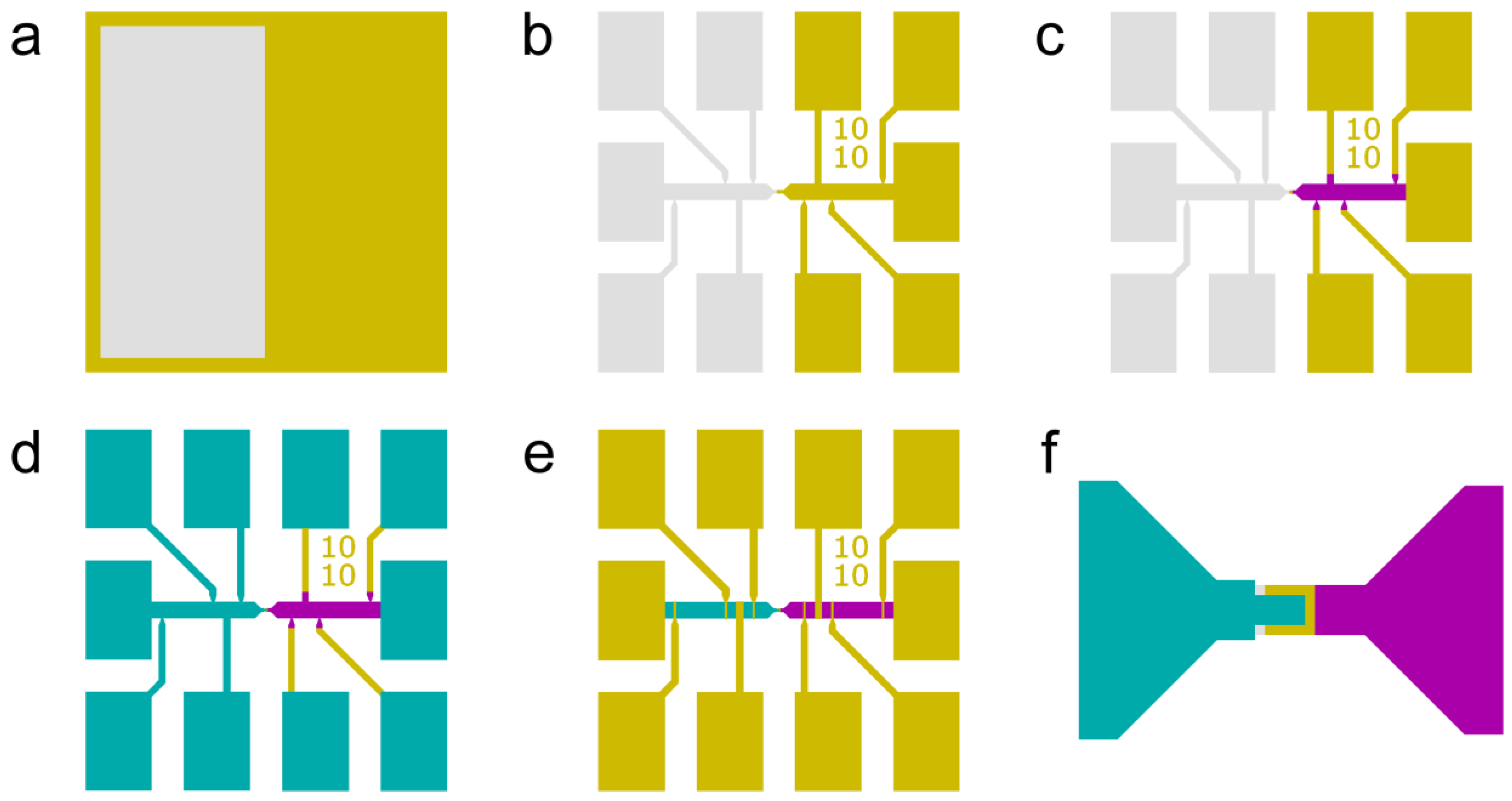
2.1. Tunnel Junction Fabrication

The method for making tunnel junctions begins with trilayers grown by the ALL-MBE technique. Our atomic fluxes are produced by Knudsen cells, all aimed at one central point where the 10 mm × 10 mm × 1 mm single crystal substrates we grow on are held. The substrates are maintained at a temperature that allows sufficient thermal energy for the incoming atoms to move laterally on the surface of the growing film and find their place within the developing crystal structure but not enough thermal energy that diffusion of atoms throughout the thickness of the film takes place. Oxygen is the only element not deposited in this way and is instead introduced into the film during the growth using pure distilled ozone, a powerful oxidizer. Reflection high energy electron diffraction (RHEED) monitors the crystal structure during growth, providing the real-time feedback the MBE operator uses to steer the growth. Low deposition rates and computer-controlled shuttering of the cells provide fine control over the entire process to better than 1%. This precise control over the stoichiometry of each layer enables the atomic layer-by-layer growth mode necessary for producing heterostructures with sharp interfaces between specifically designed blocks of materials.
The substrates used in this work are single-crystal LaSrAlO4 (LSAO) with a (001) orientation. The a-axis lattice constant of LSAO is very close to the a- and b-axis lattice constants of LSCO, which coerces the cuprate layers to grow tetragonally along the c-axis. At the beginning of each film growth, a thin (0.51.0 unit cell) buffer layer of overdoped LSCO is first deposited to initiate good growth. The upper and lower sections of the subsequently deposited trilayers are composed of LSCO, with the middle barrier layer being made from LCO, similar to Ref. [71]. One difference between that study and more recent work [73,74] is that many different junctions with an assortment of strontium contents that range from slightly undoped (x = 0.10) to optimal doping (x = 0.16) have been made. Additionally, different barrier thicknesses down to 0.5 unit cells have been tested. The last step of each growth is to cap the trilayers, in situ, with a thin layer of gold to protect the surface from the atmosphere.
The first step when making these junctions is to define the overall shape of the bottom electrodes. Since we are making c-axis junctions, we cannot easily contact the bottom of the junction as it is anchored to the substrate. Instead, part of the bottom layer of the trilayer serves as one pair of our current and voltage electrodes. The photolithography mask pattern is shown in Figure 1a. After creating this geometry in photoresist on the surface of the trilayer, the pattern is transferred into the film by argon ion milling with a 500 V beam voltage and 2.5 mA/cm2 ion beam current density.
Once the bottom electrode geometry is defined, we thin those areas that serve as the electrodes while maintaining the trilayer structure of the junction. A round mesa is patterned for the junction area while the trilayer outside of the mesa is thinned by ion milling through the top and middle layers, leaving as much of the bottom layer as possible (Figure 1b). Using a reduced beam voltage and current density so that the etch rate is slower helps with this. Additionally, the thickness of the “dead layer” resulting from ion milling damage can be minimized. The bonding pad areas are not etched, so the pads are thicker and more robust.
Contacts to the top of the mesa are made with gold, but before we can do that, the area around the mesa must be insulated so that the gold does not short the top and bottom of the junction. A double-layer resist process and the mask shown in Figure 1c is used to expose the entire bottom electrode and sides of the mesa and define vias on the top. The exposed in situ gold is removed by wet etching, and then Al2O3 is deposited by e-beam evaporation and liftoff. The Al2O3 thickness should be at least the same as the depth that was etched through while making the bottom electrode. A subsequent double-layer resist photolithography process, evaporation of gold, and liftoff define the top electrodes and bonding pads (Figure 1d). Typical gold thickness is 100–200 nm, much larger than the Al2O3 thickness to cover the Al2O3 step sufficiently. While the images shown in Figure 1 only illustrate the creation of one device, in practice, the actual lithography mask contains many copies (of the order 100) of each design with various mesa diameters.

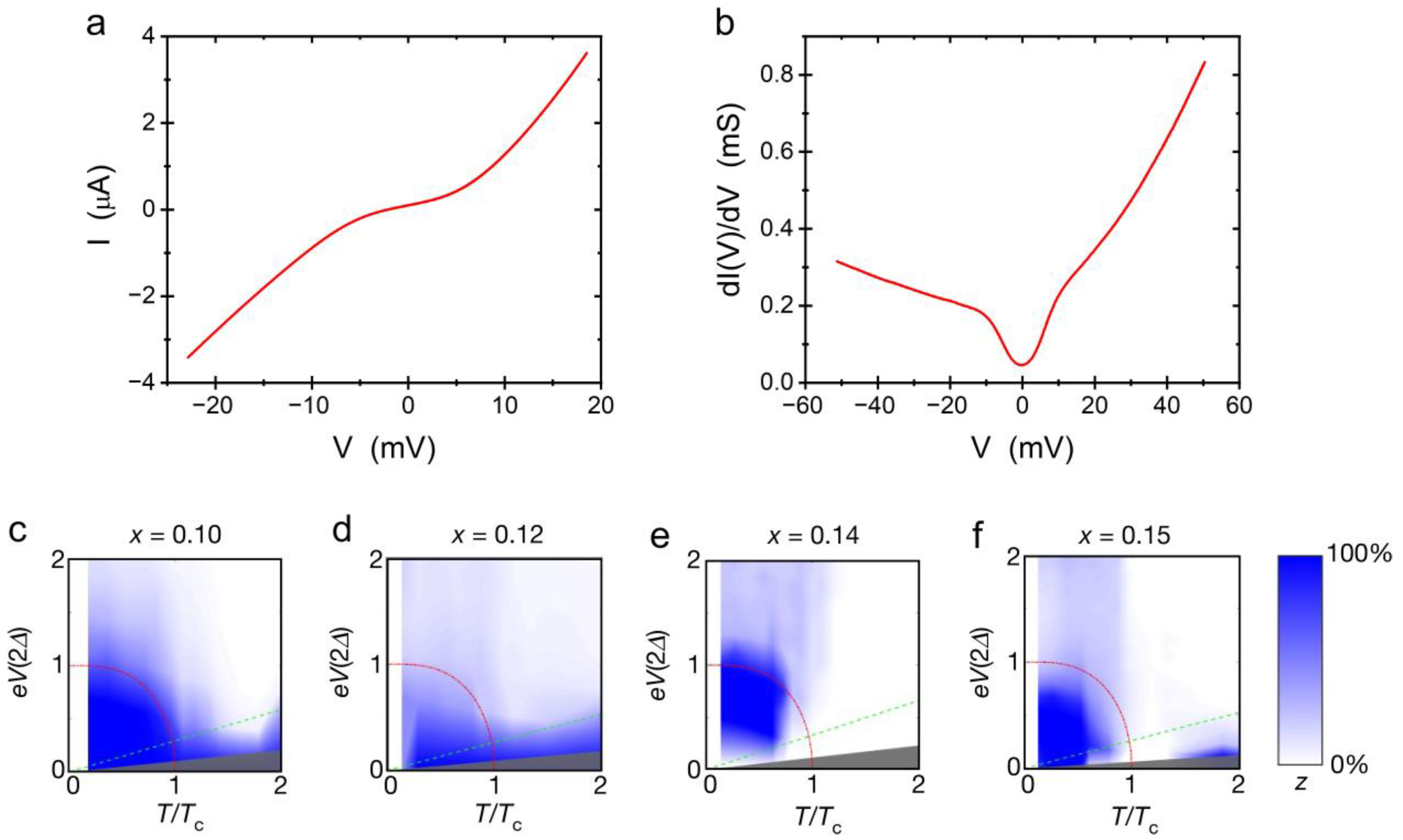
2.2. Tunnel Junction Results

Representative electrical transport data for a high-Tc tunnel junction are shown in Figure 2. Based on the previous measurements in Ref. [71], we expected that we should not observe any supercurrent tunneling across these junctions, which was indeed confirmed in the current–voltage, I(V), measurements. The differential conductance shows a dip near zero bias but does not go to zero, even at the lowest temperatures. At biases outside this pseudogap, the I(V) is non-linear, as observed in other tunneling experiments involving the high-Tc cuprates [73,74,75,76,77].
Novel results came from shot-noise measurements with these junctions that were used to determine the charge of carriers in the electrodes [73]. At temperatures far above Tc, the noise power spectral density followed the expected 2eIcoth(eV/2kBT) dependence for single electron tunneling. However, as the temperature approached Tc, excess noise was detected, which was attributed to pair tunneling. Fits to the combined function (1 − z) × 2eIcoth(eV/2kBT) + z × 4eIcoth(eV/kBT) that uses the fraction of pair tunneling, z, as a fitting parameter, quantified this excess noise. Not only was pair tunneling observed above Tc, but also below Tc for voltages outside the gap, V > Δ. This was true of all doping levels used for the upper and lower electrodes (x = 0.100.15).

3. Josephson Junctions

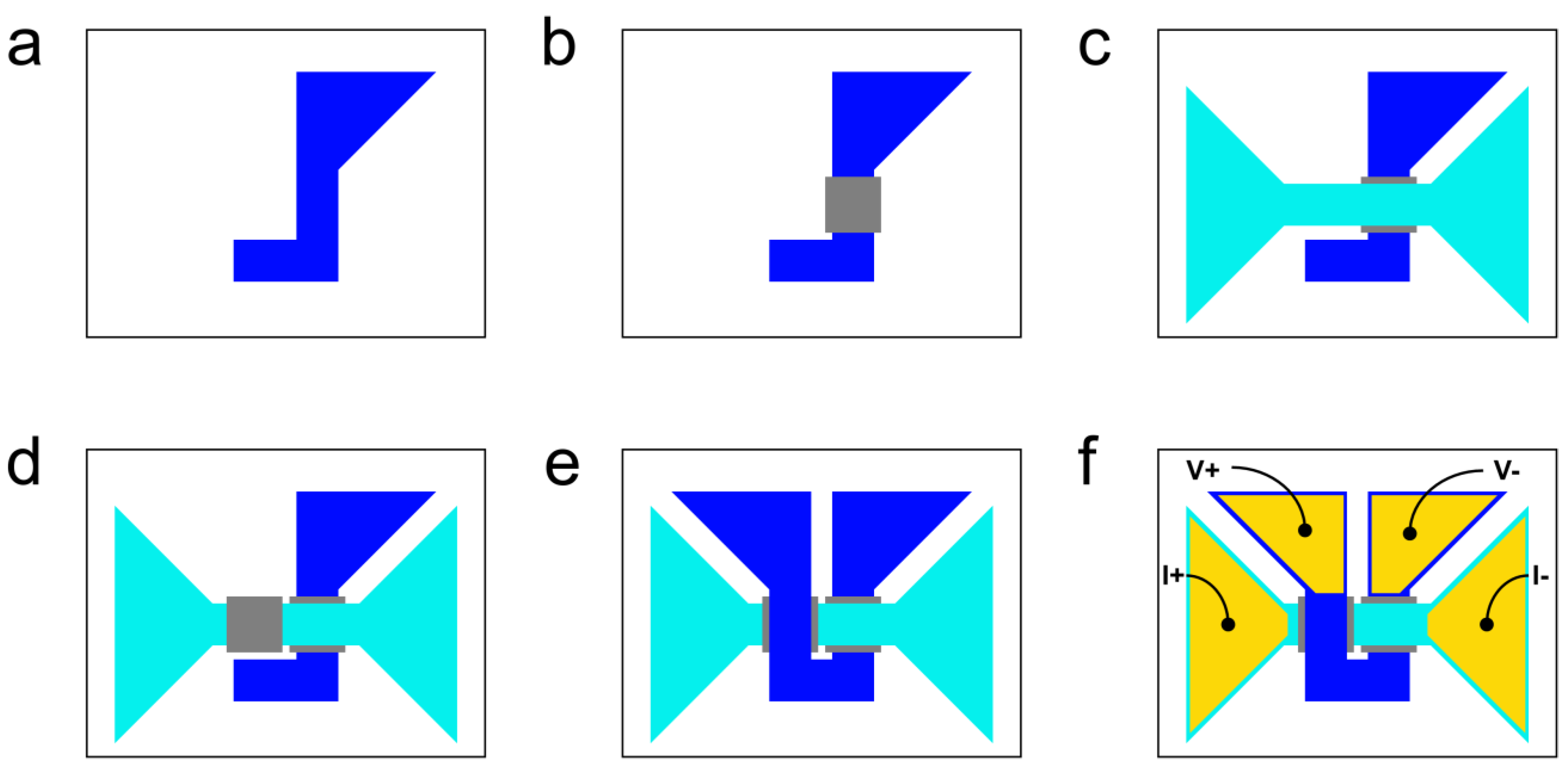
3.1. Josephson Junction Fabrication

Junctions based on an LCO barrier are unsuitable for fabricating c-axis high-Tc superconductor S-I-S Josephson junctions. The focus of our current research in this area is the exploration of different non-cuprate complex oxides that could provide a suitable barrier that would allow coherent tunneling and the observation of the Josephson effect. In this work, we have made a few improvements to the previous device geometry [78].
The first is to prepare the sample for the top electrode from the beginning. As we will see, this eliminates the need for an insulator deposition step around the entirety of the junction and possible leakage current to the bottom electrode. We start with a trilayer structure as before, although now the barrier is not LCO but some other oxide that grows epitaxially with LSCO, such as LSAO. Half of the film where the device will be created is masked off, and the other half is ion-milled completely away, all the way down and slightly into the substrate. This area is then backfilled with Al2O3 in a self-aligned manner with an Al2O3 thickness that exceeds the depth that was etched so that Al2O3 protrudes above the surface of the cuprate film (Figure 3a). The overall device geometry is then patterned into the film using photolithography and ion milling (Figure 3b). This is a more complicated design than the one presented in Section 2, with provisions for multiple contacts. These will allow for separately characterizing the upper electrodes, lower electrodes, and the junction area, as will become apparent from the following steps.
We proceed now as before by thinning the portion of the trilayer that will become the bottom electrode (Figure 3c). Reduced ion beam voltage and current density are used again to help stop at the correct depth and minimize damage to the remaining layers. Any of the multitudes of contact pads in this design could also be used for test etchings to calibrate the proper ion milling time. The final steps in this scheme involve depositing the top electrode (Figure 3d) and extra gold for bonding pads (Figure 3e). Here, we use a stack of niobium, titanium, and gold for the top electrode. The only caveat here is that the thickness of this metallization should be larger than the thickness of the Al2O3 layer deposited at the beginning that projected above the film surface so that that step is completely covered. Using a superconducting material for the top electrode eliminates the electrode resistance, measured in series with the junction when the niobium goes superconducting. This, in turn, allows for smaller junction areas to be produced as we only need to make one contact with the top of the trilayer. An additional benefit is that superconducting electrodes open the door for more complicated superconducting circuits.

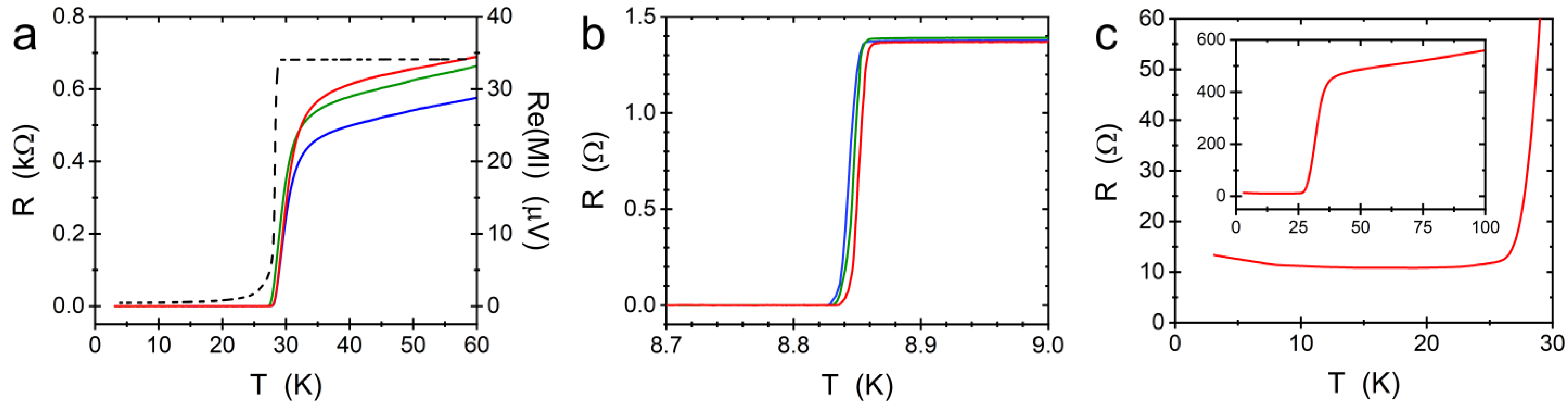
3.2. Preliminary Measurements

Several hundred devices have been fabricated to date following the above procedure. We have verified previous results using LCO as a barrier and have begun testing other complex oxides to try and observe the Josephson effect in c-axis junctions. In Figure 4, we show some results using a single stoichiometric layer as a barrier. In Figure 4a, we show the superconducting transition of a representative trilayer measured by mutual inductance immediately after film growth, i.e., before any fabrication steps were performed, and compare that to the resistive transition of the bottom electrode of some finished devices, all fabricated from the same film. The processing has not degraded the bottom electrode layers as the temperature that resistance goes to zero corresponds precisely with the temperature at which the mutual inductance signal drops or, equivalently, the temperature that screening sets in, as would be anticipated.
The superconducting transition of a few top electrodes is shown in Figure 4b. They are reproducible and reasonably close to the expected Tc of bulk niobium. Although both the top and bottom electrodes are superconducting, we still do not observe any supercurrent across the junction (Figure 4c), even for nominal barrier thicknesses as low as 6 Å. We believe that in the case of LSAO, the barrier material disrupts the superconductivity in the cuprate layers immediately next to this layer, effectively expanding the tunneling barrier [79]. Transport measurements in devices using La2ZnO4 for the barrier material have yielded similar results.
In the past, the main impediment to the reproducible fabrication of c-axis Josephson junctions was believed to be the creation of ultrathin yet pinhole-free barrier layers and sharp interfaces, which are necessary due to the extremely short c-axis coherence length in high-Tc cuprates. While the result shown in Figure 4c is not what was hoped for, it is still a testament to the perfect interfaces created by this technique that begins with ALL-MBE, as the many junctions we have tested are undoubtedly free of pinholes. Currently, finding a suitable barrier material with a good lattice match that does not deplete carriers or otherwise destroy superconductivity in the neighboring LSCO layers remains the main challenge to overcome. There are many other known insulators yet to try. Still, we must consider the possibility that the best barrier material may not naturally occur but can be created in very thin films under epitaxial strain, requiring much more time and effort to discover. Making good contacts that do not cause any heating to the top and bottom of the junctions is another issue that needs to be overcome for accurate measurements. The all-superconducting contacts presented here are a good step towards solving this problem. Still, until a noticeable Josephson effect is observed, we will not know if our top contact materials and geometry are optimized for this purpose.

4. Dyon Detectors

Proposed Dyon Detector Fabrication

Finally, we briefly discuss the possible fabrication steps involved in a detector for dyons. These exotic low-energy excitations that carry both electric and magnetic charge have been predicted to exist in underdoped cuprates [80]. By the symmetric version of Maxwell’s equations, which include magnetic charges and currents, a wire carrying a dyon current would produce a circumferential magnetic field from the electric component of the current and a circumferential electric field from the magnetic component of the current. This electric field could be detected by a coil constructed around the wire, much like a pick-up coil can detect the induced EMF of a time-varying magnetic field passing through it.
The fabrication scheme we have proposed [80] would be difficult to realize but certainly is within the realm of current technical capabilities. It relies on removing a film grown by ALL-MBE from the vacuum chamber where the growth was performed, carrying out some processing steps, and then reinserting the processed film back into the MBE chamber for subsequent growth. This procedure relies on controllably heating the sample in the presence of ozone, which cleans contaminants from the film while monitoring the condition of the surface by RHEED until a crystalline surface is again achieved. At this point, a new ALL-MBE synthesis step may take place.
Our proposed process [80] begins by growing a layer of optimally doped LSCO followed by pattering by photolithography and then ion milling to establish one side of the detecting coil (Figure 5a). The film is then reinserted into the MBE chamber where a layer of LSAO is grown. This is subsequently patterned to leave a patch of insulator on the LSCO where the (predicted) dyon carrying wire will be placed (Figure 5b). The sample goes back into the MBE chamber again, and another layer of optimally doped LSCO that will form the basis of the wire is grown. Another round of lithography and ion milling defines the dimensions of the wire as well as its contacts (Figure 5c). Once more, a layer of LSAO is grown and patterned so that a patch remains to insulate the second half of the coil (Figure 5d). The last MBE growth and successive patterning and etching creates the second half of the coil (Figure 5e), after which lithography, metallization, and liftoff create gold contact pads for the biasing and detection (Figure 5f).
As mentioned above, this is a very demanding set of steps to be followed if the dyon detection device, as proposed here, is to become a reality. Care must be taken during the ion milling steps to minimize over-etching. The subsequently deposited layers need to be thick enough to overcome step edges created by the previous microfabrication processes. This demands careful characterization of each step and coordination among all those involved in the growth and processing stages of the device creation. Nevertheless, none of the individual processes are infeasible. Creating a dyon detection device in this manner, which should give maximum sensitivity due to its minimized active area, could be realized.

5. Conclusions

In the preceding sections, we have presented methods to create devices of interest from high-Tc cuprates grown by ALL-MBE. The atomically precise interfaces are necessary for the tunnel junctions, Josephson junctions, and dyon detection devices to be realized. The procedures given here, based on ALL-MBE, for creating such structures can be easily extended to generating more complex designs, such as Josephson junction arrays, superconducting interference devices, or more sensitive dyon detection devices with multiple coils. With careful consideration and testing, they may also be suitable for a wider variety of materials.

Author Contributions

A.T.B. and I.B. conceived the microfabrication schemes. X.H. and X.X. synthesized films by atomic layer-by-layer molecular beam epitaxy. A.T.B. performed the microfabrication processing. A.T.B., X.H., R.C. and X.X. performed low-temperature electrical transport measurements. I.B. and X.S. supervised the project. A.T.B. drafted the manuscript. All authors have read and agreed to the published version of the manuscript.

Funding

This research was supported by the DOE, Basic Energy Sciences, Materials Science and Engineering Division. X.H was supported by the Gordon and Betty Moore Foundation’s EPiQS Initiative through grant GBMF9074.

Data Availability Statement

All data are available upon reasonable request.

Conflicts of Interest

The authors declare no conflict of interest.

References

  1. Bednorz, J.G.; Müller, K.A. Possible High Tc Superconductivity in the Ba−La−Cu−O System. Z. Phys. B Condens. Matter 1986, 64, 189–193. [Google Scholar] [CrossRef]
  2. Cava, R.J.; van Dover, R.B.; Batlogg, B.; Rietman, E.A. Bulk Superconductivity at 36 K in La1.8Sr0.2CuO4. Phys. Rev. Lett. 1987, 58, 408–410. [Google Scholar] [CrossRef] [PubMed] [Green Version]
  3. Wu, M.K.; Ashburn, J.R.; Torng, C.J.; Hor, P.H.; Meng, R.L.; Gao, L.; Huang, Z.J.; Wang, Y.Q.; Chu, C.W. Superconductivity at 93 K in a New Mixed-Phase Y-Ba-Cu-O Compound System at Ambient Pressure. Phys. Rev. Lett. 1987, 58, 908–910. [Google Scholar] [CrossRef] [PubMed] [Green Version]
  4. Hazen, R.M.; Prewitt, C.T.; Angel, R.J.; Ross, N.L.; Finger, L.W.; Hadidiacos, C.G.; Veblen, D.R.; Heaney, P.J.; Hor, P.H.; Meng, R.L.; et al. Superconductivity in the High-T, Bi-Ca-Sr-Cu-O System: Phase Identification. Phys. Rev. Lett. 1988, 60, 1174–1177. [Google Scholar] [CrossRef] [Green Version]
  5. Sheng, Z.Z.; Hermann, A.M. Bulk superconductivity at 120 K in the Tl-Ca/Ba-Cu-O system. Nature 1988, 332, 138–139. [Google Scholar] [CrossRef]
  6. Schilling, A.; Cantoni, M.; Guo, J.D.; Ott, H.R. Superconductivity above 130 K in the Hg-Ba-Ca-Cu-O system. Nature 1993, 363, 56–58. [Google Scholar] [CrossRef]
  7. Vaknin, D.; Sinha, S.K.; Moncton, D.E.; Johnston, D.C.; Newsam, J.M.; Safinya, C.R.; King, H.E., Jr. Antiferromagnetism in La2CuO4-y. Phys. Rev. Lett. 1987, 58, 2802–2805. [Google Scholar] [CrossRef]
  8. Mitsuda, S.; Shirane, G.; Sinha, S.K.; Johnston, D.C.; Alvarez, M.S.; Vaknin, D.; Moncton, D.E. Confirmation of antiferromagnetism in La2CuO4-y with polarized neutrons. Phys. Rev. B 1987, 36, 822–825. [Google Scholar] [CrossRef]
  9. Freltoft, T.; Remeika, J.P.; Moncton, D.E.; Cooper, A.S.; Fischer, J.E.; Harshman, D.; Shirane, G.; Sinha, S.K.; Vaknin, D. Antiferromagnetism and oxygen deficiency in single-crystal La2CuO4-δ. Phys. Rev. B 1987, 36, 826–828. [Google Scholar] [CrossRef]
  10. Tranquada, J.M.; Sternlieb, B.J.; Axe, J.D.; Nakamura, Y.; Uchida, S. Evidence for stripe correlations of spins and holes in copper oxide superconductors. Nature 1995, 375, 561–563. [Google Scholar] [CrossRef]
  11. Suzuki, T.; Goto, T.; Chiba, K.; Shinoda, T.; Fukase, T.; Kimura, H.; Yamada, K.; Ohashi, M.; Yamaguchi, Y. Observation of modulated magnetic long-range order in La1.88Sr0.12CuO4. Phys. Rev. B 1998, 57, R3229–R3232. [Google Scholar] [CrossRef]
  12. Kimura, H.; Matsushita, H.; Hirota, K.; Endoh, Y.; Yamada, K.; Shirane, G.; Lee, Y.S.; Kastner, M.A.; Birgeneau, R.J. Incommensurate geometry of the elastic magnetic peaks in superconducting La1.88Sr0.12CuO4. Phys. Rev. B 2000, 61, 14366–14369. [Google Scholar] [CrossRef] [Green Version]
  13. Lake, B.; Rønnow, H.M.; Christensen, N.B.; Aeppli, G.; Lefmann, K.; McMorrow, D.F.; Vorderwisch, P.; Smeibidl, P.; Mangkorntong, N.; Sasagawa, T.; et al. Antiferromagnetic order induced by an applied magnetic field in a high-temperature superconductor. Nature 2002, 415, 299–301. [Google Scholar] [CrossRef] [PubMed] [Green Version]
  14. Kivelson, S.A.; Bindloss, I.P.; Fradkin, E.; Oganesyan, V.; Tranquada, J.M.; Kapitulnik, A.; Howald, C. How to detect fluctuating stripes in the high-temperature superconductors. Rev. Mod. Phys. 2003, 75, 1201–1241. [Google Scholar] [CrossRef] [Green Version]
  15. Fujita, M.; Goka, H.; Yamada, K.; Tranquada, J.M.; Regnault, L.P. Stripe order, depinning and fluctuations in La1.875Ba0.125CuO4 and La1.875Ba0.075Sr0.050CuO4. Phys. Rev. B 2004, 70, 104517. [Google Scholar] [CrossRef] [Green Version]
  16. Lee, S.; Huang, E.W.; Johnson, T.A.; Guo, X.; Husain, A.A.; Mitrano, M.; Lu, K.; Zakrzewski, A.V.; de la Peña, G.A.; Peng, Y.; et al. Generic character of charge and spin density waves in superconducting cuprates. Proc. Natl. Acad. Sci. USA 2022, 119, e2119429119. [Google Scholar] [CrossRef]
  17. Hoffman, J.E.; Hudson, E.W.; Lang, K.M.; Madhavan, V.; Eisaki, H.; Uchida, S.; Davis, J.C. A Four Unit Cell Periodic Pattern of Quasi-Particle States Surrounding Vortex Cores in Bi2Sr2CaCu2O8+δ. Science 2002, 295, 466–469. [Google Scholar] [CrossRef] [Green Version]
  18. Abbamonte, P.; Rusydi, A.; Smadici, S.; Gu, G.D.; Sawatzky, G.A.; Feng, D.L. Spatially modulated ‘Mottness’ in La2-xBaxCuO4. Nat. Phys. 2005, 1, 15–158. [Google Scholar] [CrossRef]
  19. Wise, W.D.; Boyer, M.C.; Chatterjee, K.; Kondo, T.; Takeuchi, T.; Ikuta, H.; Wang, Y.; Hudson, E.W. Charge-density-wave origin of cuprate checkerboard visualized by scanning tunnelling microscopy. Nat. Phys. 2008, 4, 696–699. [Google Scholar] [CrossRef]
  20. Parker, C.V.; Aynajian, P.; da Silva Neto, E.H.; Pushp, A.; Ono, S.; Wen, J.; Xu, Z.; Gu, G.; Yazdani, A. Fluctuating stripes at the onset of the pseudogap in the high-Tc superconductor Bi2Sr2CaCu2O8+x. Nature 2010, 468, 677–680. [Google Scholar] [CrossRef]
  21. Wu, T.; Mayaffre, H.; Krämer, S.; Horvatić, M.; Berthier, C.; Hardy, W.N.; Liang, R.; Bonn, D.A.; Julien, M.-H. Magnetic-field-induced charge-stripe order in the high-temperature superconductor YBa2Cu3Oy. Nature 2011, 477, 191–194. [Google Scholar] [CrossRef] [PubMed] [Green Version]
  22. Ghiringhelli, G.; Le Tacon, M.; Minola, M.; Blanco-Canosa, S.; Mazzoli, C.; Brookes, N.B.; De Luca, G.M.; Frano, A.; Hawthorn, D.G.; He, F.; et al. Long-Range Incommensurate Charge Fluctuations in (Y,Nd)Ba2Cu3O6+x. Science 2012, 337, 821–825. [Google Scholar] [CrossRef] [PubMed] [Green Version]
  23. Chang, J.; Blackburn, E.; Holmes, A.T.; Christensen, N.B.; Larsen, J.; Mesot, J.; Liang, R.; Bonn, D.A.; Hardy, W.N.; Watenphul, A.; et al. Direct observation of competition between superconductivity and charge density wave order in YBa2Cu3O6.67. Nat. Phys. 2012, 8, 871–876. [Google Scholar] [CrossRef] [Green Version]
  24. Torchinsky, D.; Mahmood, F.; Bollinger, A.T.; Božović, I.; Gedik, N. Fluctuating charge-density waves in a cuprate superconductor. Nat. Mater. 2013, 12, 387–391. [Google Scholar] [CrossRef] [PubMed] [Green Version]
  25. Miao, H.; Lorenzana, J.; Seibold, G.; Peng, Y.Y.; Amorese, A.; Yakhou-Harris, F.; Kummer, K.; Brookes, N.B.; Konik, R.M.; Thampy, V.; et al. High-temperature charge density wave correlations in La1.875Ba0.125CuO4 without spin–charge locking. Proc. Natl. Acad. Sci. USA 2017, 114, 12430–12435. [Google Scholar] [CrossRef] [Green Version]
  26. Miao, H.; Ishikawa, D.; Heid, R.; Le Tacon, M.; Fabbris, G.; Meyers, D.; Gu, G.D.; Baron, A.Q.R.; Dean, M.P.M. Incommensurate Phonon Anomaly and the Nature of Charge Density Waves in Cuprates. Phys. Rev. X 2018, 8, 011008. [Google Scholar] [CrossRef] [Green Version]
  27. Miao, H.; Fumagalli, R.; Rossi, M.; Lorenzana, J.; Seibold, G.; Yakhou-Harris, F.; Kummer, K.; Brookes, N.B.; Gu, G.D.; Braicovich, L.; et al. Formation of Incommensurate Charge Density Waves in Cuprates. Phys. Rev. X 2019, 9, 031042. [Google Scholar] [CrossRef] [Green Version]
  28. Miao, H.; Fabbris, G.; Koch, R.J.; Mazzone, D.G.; Nelson, C.S.; Acevedo-Esteves, R.; Gu, G.D.; Li, Y.; Yilmaz, T.; Kaznatcheev, K.; et al. Charge density waves in cuprate superconductors beyond the critical doping. NPJ Quantum Mater. 2021, 6, 31. [Google Scholar] [CrossRef]
  29. Mirzaei, S.I.; Stricker, D.; Hancock, J.N.; Berthod, C.; Georges, A.; van Heumen, E.; Chan, M.K.; Zhao, X.; Li, Y.; Greven, M.; et al. Spectroscopic evidence for Fermi liquid-like energy and temperature dependence of the relaxation rate in the pseudogap phase of the cuprates. Proc. Natl. Acad. Sci. USA 2013, 110, 5774–5778. [Google Scholar] [CrossRef] [Green Version]
  30. Barišić, N.; Chan, M.K.; Li, Y.; Yu, G.; Zhao, X.; Dressel, M.; Smontara, A.; Greven, M. Universal sheet resistance and revised phase diagram of the cuprate high-temperature superconductors. Proc. Natl. Acad. Sci. USA 2013, 110, 12235–12240. [Google Scholar] [CrossRef]
  31. Li, Y.; Tabis, W.; Yu, G.; Barišić, N.; Greven, M. Hidden Fermi-liquid Charge Transport in the Antiferromagnetic Phase of the Electron-Doped Cuprate Superconductors. Phys. Rev. Lett. 2016, 117, 197001. [Google Scholar] [CrossRef] [PubMed] [Green Version]
  32. Proust, C.; Vignolle, B.; Levallois, J.; Adachi, S.; Hussey, N.E. Fermi liquid behavior of the in-plane resistivity in the pseudogap state of YBa2Cu4O8. Proc. Natl. Acad. Sci. USA 2016, 113, 13654–13659. [Google Scholar] [CrossRef] [PubMed] [Green Version]
  33. Cooper, R.A.; Wang, Y.; Vignolle, B.; Lipscombe, O.J.; Hayden, S.M.; Tanabe, Y.; Adachi, T.; Koike, Y.; Nohara, M.; Takagi, H.; et al. Anomalous Criticality in the Electrical Resistivity of La2−xSrxCuO4. Science 2009, 323, 603–607. [Google Scholar] [CrossRef]
  34. Bruin, J.A.N.; Sakai, H.; Perry, R.S.; Mackenzie, A.P. Similarity of Scattering Rates in Metals Showing T-linear Resistivity. Science 2013, 339, 804–807. [Google Scholar] [CrossRef] [PubMed]
  35. Giraldo-Gallo, P.; Galvis, J.A.; Stegen, Z.; Modic, K.A.; Balakirev, F.F.; Betts, J.B.; Lian, X.; Moir, C.; Riggs, S.C.; Wu, J.; et al. Scale-invariant magnetoresistance in a cuprate superconductor. Science 2018, 361, 479–481. [Google Scholar] [CrossRef] [Green Version]
  36. Legros, A.; Benhabib, S.; Tabis, W.; Laliberté, F.; Dion, M.; Lizaire, M.; Vignolle, B.; Vignolles, D.; Raffy, H.; Li, Z.Z.; et al. Universal T-linear resistivity and Planckian dissipation in overdoped cuprates. Nat. Phys. 2019, 15, 142–147. [Google Scholar] [CrossRef] [Green Version]
  37. Greene, R.L.; Mandal, P.R.; Poniatowski, N.R.; Sarkar, T. The Strange Metal State of the Electron-Doped Cuprates. Annu. Rev. Condens. Matter Phys. 2020, 11, 213–229. [Google Scholar] [CrossRef] [Green Version]
  38. Varma, C.M. Linear in temperature resistivity and associated mysteries including high temperature superconductivity. Rev. Mod. Phys. 2020, 92, 031001. [Google Scholar] [CrossRef]
  39. Putzke, C.; Benhabib, S.; Tabis, W.; Ayres, J.; Wang, Z.; Malone, L.; Licciardello, S.; Lu, J.; Kondo, T.; Takeuchi, T.; et al. Reduced Hall carrier density in the overdoped strange metal regime of cuprate superconductors. Nat. Phys. 2021, 17, 826–831. [Google Scholar] [CrossRef]
  40. Ayres, J.; Berben, M.; Čulo, M.; Hsu, Y.-T.; van Heumen, E.; Huang, Y.; Zaanen, J.; Kondo, T.; Takeuchi, T.; Cooper, J.R.; et al. Incoherent transport across the strange-metal regime of overdoped cuprates. Nature 2021, 595, 661–666. [Google Scholar] [CrossRef]
  41. Ando, Y.; Segawa, K.; Komiya, S.; Lavrov, A.N. Electrical Resistivity Anisotropy from Self-Organized One Dimensionality in High-Temperature Superconductors. Phys. Rev. Lett. 2002, 88, 137005. [Google Scholar] [CrossRef] [PubMed] [Green Version]
  42. Abdel-Jawad, M.; Kennett, M.P.; Balicas, L.; Carrington, A.; Mackenzie, A.P.; McKenzie, R.H.; Hussey, N.E. Anisotropic scattering and anomalous normal-state transport in a high-temperature superconductor. Nat. Phys. 2006, 2, 821–825. [Google Scholar] [CrossRef] [Green Version]
  43. Hinkov, V.; Haug, D.; Fauqué, B.; Bourges, P.; Sidis, Y.; Ivanov, A.; Bernhard, C.; Lin, C.T.; Keimer, B. Electronic Liquid Crystal State in the High-Temperature Superconductor YBa2Cu3O6.45. Science 2008, 319, 597–600. [Google Scholar] [CrossRef] [PubMed] [Green Version]
  44. Lawler, M.J.; Fujita, K.; Lee, J.; Schmidt, A.R.; Kohsaka, Y.; Kim, C.K.; Eisaki, H.; Uchida, S.; Davis, J.C.; Sethna, J.P.; et al. Intra-unit-cell electronic nematicity of the high-Tc copper-oxide pseudogap states. Nature 2010, 466, 347–351. [Google Scholar] [CrossRef] [Green Version]
  45. Daou, R.; Chang, J.; LeBoeuf, D.; Cyr-Choinière, O.; Laliberté, F.; Doiron-Leyraud, N.; Ramshaw, B.J.; Liang, R.; Bonn, D.A.; Hardy, W.N.; et al. Broken rotational symmetry in the pseudogap phase of a high-Tc superconductor. Nature 2010, 463, 519–522. [Google Scholar] [CrossRef] [PubMed] [Green Version]
  46. Fradkin, E.; Kivelson, S.A.; Lawler, M.J.; Eisenstein, J.P.; Mackenzie, A.P. Nematic Fermi Fluids in Condensed Matter Physics. Annu. Rev. Cond. Matter Phys. 2010, 1, 153–178. [Google Scholar] [CrossRef] [Green Version]
  47. Fujita, K.; Kim, C.K.; Lee, I.; Hamidian, M.H.; Firmo, I.A.; Mukhopadhyay, S.; Eisaki, H.; Uchida, S.; Lawler, M.J.; Kim, E.-A.; et al. Simultaneous Transitions in Cuprate Momentum-Space Topology and Electronic Symmetry Breaking. Science 2014, 344, 612–616. [Google Scholar] [CrossRef] [Green Version]
  48. Lubashevsky, Y.; Pan, L.D.; Kirzhner, T.; Koren, G.; Armitage, N.P. Optical Birefringence and Dichroism of Cuprate Superconductors in the THz Regime. Phys. Rev. Lett. 2014, 112, 147001. [Google Scholar] [CrossRef] [Green Version]
  49. Cyr-Choinière, O.; Grissonnanche, G.; Badoux, S.; Day, J.; Bonn, D.A.; Hardy, W.N.; Liang, R.; Doiron-Leyraud, N.; Taillefer, L. Two types of nematicity in the phase diagram of the cuprate superconductor YBa2Cu3Oy. Phys. Rev. B 2015, 92, 224502. [Google Scholar] [CrossRef] [Green Version]
  50. Zhang, J.; Levenson-Falk, E.M.; Ramshaw, B.J.; Bonn, D.A.; Liang, R.; Hardy, W.N.; Hartnoll, S.A.; Kapitulnik, A. Anomalous thermal diffusivity in underdoped YBa2Cu3O6+x. Proc. Natl. Acad. Sci. USA 2017, 114, 5378–5383. [Google Scholar] [CrossRef]
  51. Zhao, L.; Belvin, C.A.; Liang, R.; Bonn, D.A.; Hardy, W.N.; Armitage, N.P.; Hsieh, D.A. A global inversion-symmetry-broken phase inside the pseudogap region of YBa2Cu3Oy. Nat. Phys. 2017, 13, 250–254. [Google Scholar] [CrossRef]
  52. Sato, Y.; Kasahara, S.; Murayama, H.; Kasahara, Y.; Moon, E.-G.; Nishizaki, T.; Loew, T.; Porras, J.; Keimer, B.; Shibauchi, T.; et al. Thermodynamic evidence for a nematic phase transition at the onset of the pseudogap in YBa2Cu3Oy. Nat. Phys. 2017, 13, 1074–1078. [Google Scholar] [CrossRef] [Green Version]
  53. Wu, J.; Bollinger, A.T.; He, X.; Božović, I. Spontaneous breaking of rotational symmetry in copper oxide superconductors. Nature 2017, 547, 432–435. [Google Scholar] [CrossRef] [PubMed]
  54. Ohtomo, A.; Hwang, H.Y. A high-mobility electron gas at the LaAlO3/SrTiO3 heterointerface. Nature 2004, 427, 423–426. [Google Scholar] [CrossRef] [PubMed]
  55. Tsukazaki, A.; Ohtomo, A.; Kita, A.T.; Ohno, Y.; Ohno, H.; Kawasaki, M. Quantum Hall Effect in Polar Oxide Heterostructures. Science 2007, 315, 1388–1391. [Google Scholar] [CrossRef]
  56. Brinkman, A.; Huijben, M.; van Zalk, M.; Huijben, J.; Zeitler, U.; Maan, J.C.; van der Wiel, W.G.; Rijnderss, G.; Blank, D.H.A.; Hilgenkamp, H. Magnetic effects at the interface between non-magnetic oxides. Nat. Mater. 2007, 6, 493–496. [Google Scholar] [CrossRef]
  57. Reyren, N.; Thiel, S.; Caviglia, A.D.; Kourkoutis, L.F.; Hammerl, G.; Richter, C.; Schneider, C.W.; Kopp, T.; Rüetschi, A.-S.; Jaccard, D.; et al. Superconducting Interfaces Between Insulating Oxides. Science 2007, 317, 1196–1199. [Google Scholar] [CrossRef] [PubMed]
  58. Bhattacharya, A.; May, S.J.; te Velthuis, S.G.E.; Warusawithana, M.; Zhai, X.; Jiang, B.; Zuo, J.-M.; Fitzsimmons, M.R.; Bader, S.D.; Eckstein, J.N. Metal-Insulator Transition and Its Relation to Magnetic Structure in (LaMnO3)2n/(SrMnO3)n Superlattices. Phys. Rev. Lett. 2008, 100, 257203. [Google Scholar] [CrossRef] [Green Version]
  59. Gozar, A.; Logvenov, G.; Fitting Kourkoutis, L.; Bollinger, A.T.; Giannuzzi, L.A.; Muller, D.A.; Bozovic, I. High-temperature interface superconductivity between metallic and insulating copper oxides. Nature 2008, 455, 782–785. [Google Scholar] [CrossRef] [Green Version]
  60. Wu, J.; Pelleg, O.; Logvenov, G.; Bollinger, A.T.; Sun, Y.-J.; Boebinger, G.S.; Vanević, M.; Radović, Z.; Božović, I. Anomalous independence of interface superconductivity from carrier density. Nat. Mater. 2013, 12, 877–881. [Google Scholar] [CrossRef]
  61. Butko, V.Y.; Logvenov, G.; Božović, N.; Radović, Z.; Božović, I. Madelung Strain in Cuprate Superconductors—A Route to Enhancement of the Critical Temperature. Adv. Mater. 2009, 21, 3644–3648. [Google Scholar] [CrossRef]
  62. Logvenov, G.; Gozar, A.; Bozovic, I. High-Temperature Superconductivity in a Single Copper-Oxygen Plane. Science 2009, 326, 699–702. [Google Scholar] [CrossRef]
  63. Smadici, S.; Lee, J.C.T.; Wang, S.; Abbamonte, P.; Logvenov, G.; Gozar, A.; Deville Cavellin, C.; Bozovic, I. Superconducting Transition at 38 K in Insulating-Overdoped La2CuO4−La1.64Sr0.36CuO4 Superlattices: Evidence for Interface Electronic Redistribution from Resonant Soft X-ray Scattering. Phys. Rev. Lett. 2009, 102, 107004. [Google Scholar] [CrossRef] [Green Version]
  64. Ginzburg, V.L. On surface superconductivity. Phys. Lett. 1964, 13, 101–102. [Google Scholar] [CrossRef]
  65. Kivelson, S.A. Making high Tc higher: A theoretical proposal. Phys. B Condens. Matter 2002, 318, 61–67. [Google Scholar] [CrossRef] [Green Version]
  66. Dzhumanov, S.; Solovjov, A.L.; Vovk, R.V.; Grinyov, B.V.; Djumanov, S.S. The possibility of realizing room-temperature superconductivity in High-Tc cuprates in their two-dimensional sandwich layers. Funct. Mater. 2022, 29, 475–480. [Google Scholar] [CrossRef]
  67. Bozovic, I.; Eckstein, J.N.; Virshup, G.F.; Chaiken, A.; Wall, M.; Howell, R.; Fluss, M. Atomic-Layer Engineering of Cuprate Superconductors. J. Supercond. 1994, 7, 187–195. [Google Scholar] [CrossRef]
  68. Schlom, D.G.; Harris, J.S., Jr. MBE Growth of High Tc Superconductors. In Molecular Beam Epitaxy; Farrow, R.F.C., Ed.; Noyes Publications: Park Ridge, NJ, USA, 1995; pp. 504–622. [Google Scholar] [CrossRef]
  69. Bozovic, I. Atomic-Layer Engineering of Superconducting Oxides: Yesterday, Today, Tomorrow. IEEE Trans. Appl. Supercond. 2001, 11, 2686–2695. [Google Scholar] [CrossRef]
  70. Bollinger, A.T.; Božović, I. Two-dimensional superconductivity in the cuprates revealed by atomic-layer-by-layer molecular beam epitaxy. Supercond. Sci. Technol. 2016, 29, 103001. [Google Scholar] [CrossRef]
  71. Bozovic, I.; Logvenov, G.; Verhoeven, M.A.J.; Caputo, P.; Goldobin, E.; Geballe, T.H. No mixing of superconductivity and antiferromagnetism in a high-temperature superconductor. Nature 2003, 422, 873–875. [Google Scholar] [CrossRef]
  72. Bozovic, I.; Logvenov, G.; Verhoeven, M.A.J.; Caputo, P.; Goldobin, E.; Beasley, M.R. Giant Proximity Effect in Cuprate Superconductors. Phys. Rev. Lett. 2004, 93, 157002. [Google Scholar] [CrossRef] [PubMed] [Green Version]
  73. Zhou, P.; Chen, L.; Liu, Y.; Sochnikov, I.; Bollinger, A.T.; Han, M.-G.; Zhu, Y.; He, X.; Božović, I.; Natelson, D. Electron pairing in the pseudogap state revealed by shot noise in copper oxide junctions. Nature 2019, 572, 493–496. [Google Scholar] [CrossRef] [PubMed]
  74. Zhou, P.; Chen, L.; Sochnikov, I.; Wu, T.C.; Foster, M.S.; Bollinger, A.T.; He, X.; Božović, I.; Natelson, D. Tunneling spectroscopy of c-axis epitaxial cuprate junctions. Phys. Rev. B 2020, 101, 224512. [Google Scholar] [CrossRef]
  75. Ozyuzer, L.; Zasadzinski, J.F.; Kendziora, C.; Gray, K.E. Quasiparticle and Josephson tunneling of overdoped Bi2Sr2CaCu2O8+δ. Phys. Rev. B 1999, 61, 3629–3640. [Google Scholar] [CrossRef] [Green Version]
  76. Sharoni, A.; Koren, G.; Millo, O. Correlation of tunneling spectra with surface nanomorphology and doping in thin YBa2Cu3O7−δ. EPL 2001, 54, 675–681. [Google Scholar] [CrossRef] [Green Version]
  77. Zhao, H.; Ren, Z.; Rachmilowitz, B.; Schneeloch, J.; Zhong, R.; Gu, G.; Wang, Z.; Zeljkovic, I. Charge-stripe crystal phase in an insulating cuprate. Nat. Mater. 2019, 18, 103–107. [Google Scholar] [CrossRef] [Green Version]
  78. Bollinger, A.T.; He, X.; Xu, X.; Shi, X.; Božović, I. Method to create cuprate tunnel junctions with atomically sharp interfaces. J. Vac. Sci. Technol. B 2022, 40, 015001. [Google Scholar] [CrossRef]
  79. Xu, X.; He, X.; Bollinger, A.T.; Han, M.-G.; Zhu, Y.; Shi, X.; Božović, I. A method to probe the interfaces in La2-xSrxCuO4-LaSrAlO4-La2-xSrxCuO4 trilayer junctions. Condens. Matter, 2023; submitted. [Google Scholar]
  80. Diamantini, M.C.; Trugenberger, C.A.; Bollinger, A.T.; Vinokur, V.M.; Božović, I. Topological Model of the Pseudogap State: Experimental Signatures. Front. Phys. 2022, 9, 756760. [Google Scholar] [CrossRef]
Figure 1. Fabrication scheme for creating high-Tc cuprate tunnel junctions. Gold color represents gold, magenta is the bottom LSCO layer, cyan is the top LSCO layer, and grey is the Al2O3 insulation. Pictures show the top view of the device after each step. (a) Overall bottom electrode shape after the first ion milling step. (b) Creation of bottom electrodes and mesa structure. (c) Insulating layer deposited over bottom electrodes. (d) Gold contacts with the top of the mesa.
Condensedmatter 08 00014 g001
Figure 2. Transport data for tunnel junctions. (a) Representative current–voltage and (b) differential conductance curves. (cf) Fraction of tunneling from paired carriers determined from shot noise measurements as a function of temperature and voltage for samples with differently doped top and bottom electrodes. Adapted from Ref. [73].
Condensedmatter 08 00014 g002
Figure 3. Fabrication scheme for creating high-Tc Josephson junctions. Gold color represents gold, magenta is the bottom LSCO layer, cyan is the top electrode, and grey is the Al2O3 insulation. Pictures are a top view of the device after each step. (a) Replacement of half of the cuprate film by Al2O3 in preparation for the top electrode. (b) Defining overall device shape. (c) Creation of bottom electrode. (d) Deposition of top electrode metallization. (e) Deposition of gold contacts and bonding pads. (f) Zoomed-in view of Josephson device area after all fabrication steps are finished. Adapted from Ref. [78].
Condensedmatter 08 00014 g003
Figure 4. Preliminary results with latest attempts at Josephson devices with LSAO barriers. (a) The superconducting transition of a trilayer after growth was measured by mutual inductance (dashed line). This is compared to resistive transitions of some bottom electrodes after all fabrication steps were completed (solid lines). (b) Transitions of several top electrodes. (c) Resistance of a representative junction shows a transition due to the bottom electrode but does not go to zero and increases with cooling.
Condensedmatter 08 00014 g004
Figure 5. Proposed fabrication steps for creating a dyon detection device. (a) Patterning LSCO to form one side of the detection coil. (b) Creating a patch of LSAO to insulate the right side of the coil from the wire made in the next step. (c) Creating the LSCO wire that will be used to drive current. (d) Creating another patch of LSAO to insulate the wire from the left side of the coil that is made next. (e) Patterning LSCO to form the left half of the coil. (f) Deposition of bonding pads. Adapted from Ref. [80].
Condensedmatter 08 00014 g005
Disclaimer/Publisher’s Note: The statements, opinions and data contained in all publications are solely those of the individual author(s) and contributor(s) and not of MDPI and/or the editor(s). MDPI and/or the editor(s) disclaim responsibility for any injury to people or property resulting from any ideas, methods, instructions or products referred to in the content.

