Proximity Array Device: A Novel Photon Detector Working in Long Wavelengths

 ,
,  , ,
, ,  ,
, 

Abstract
:1. Introduction
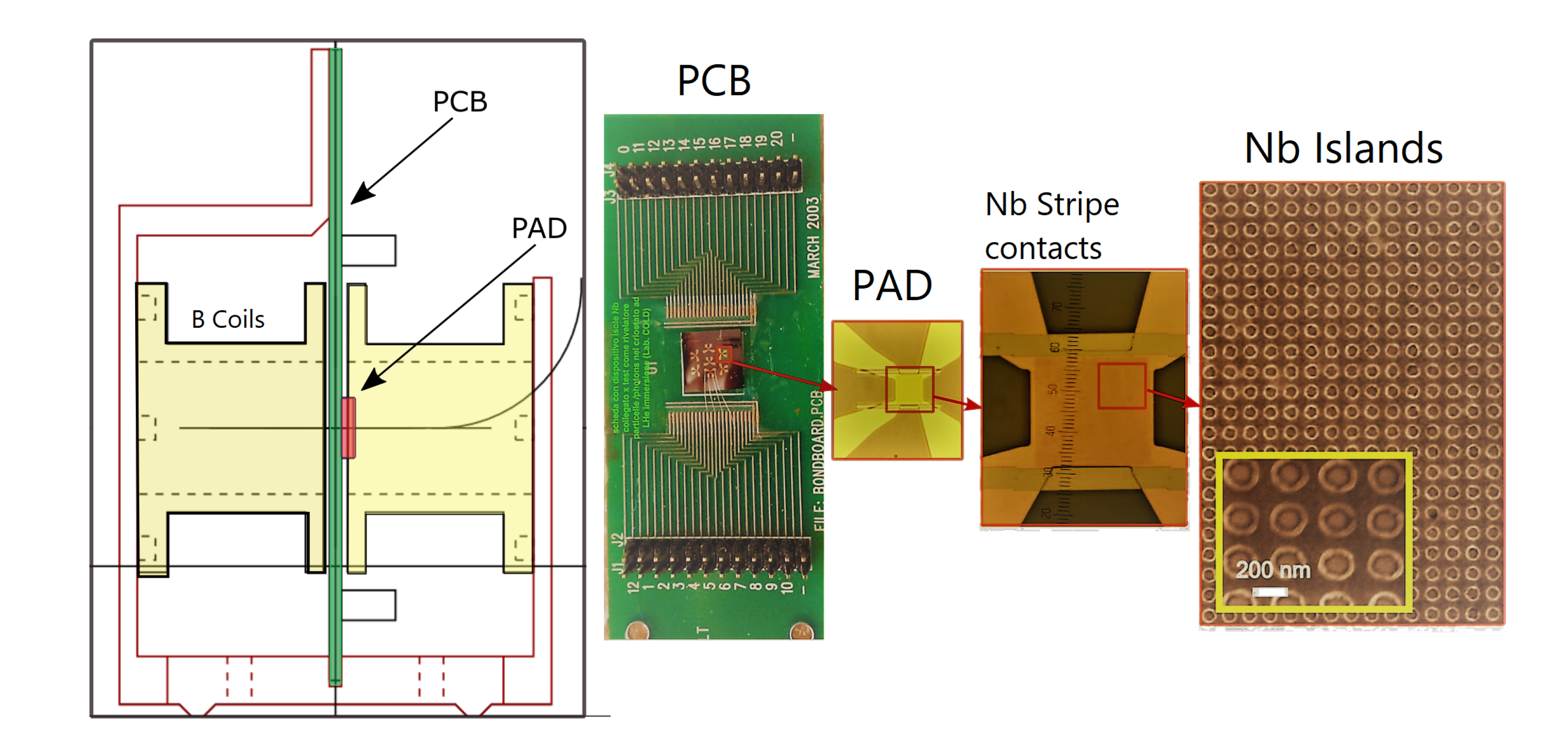
2. Experiment
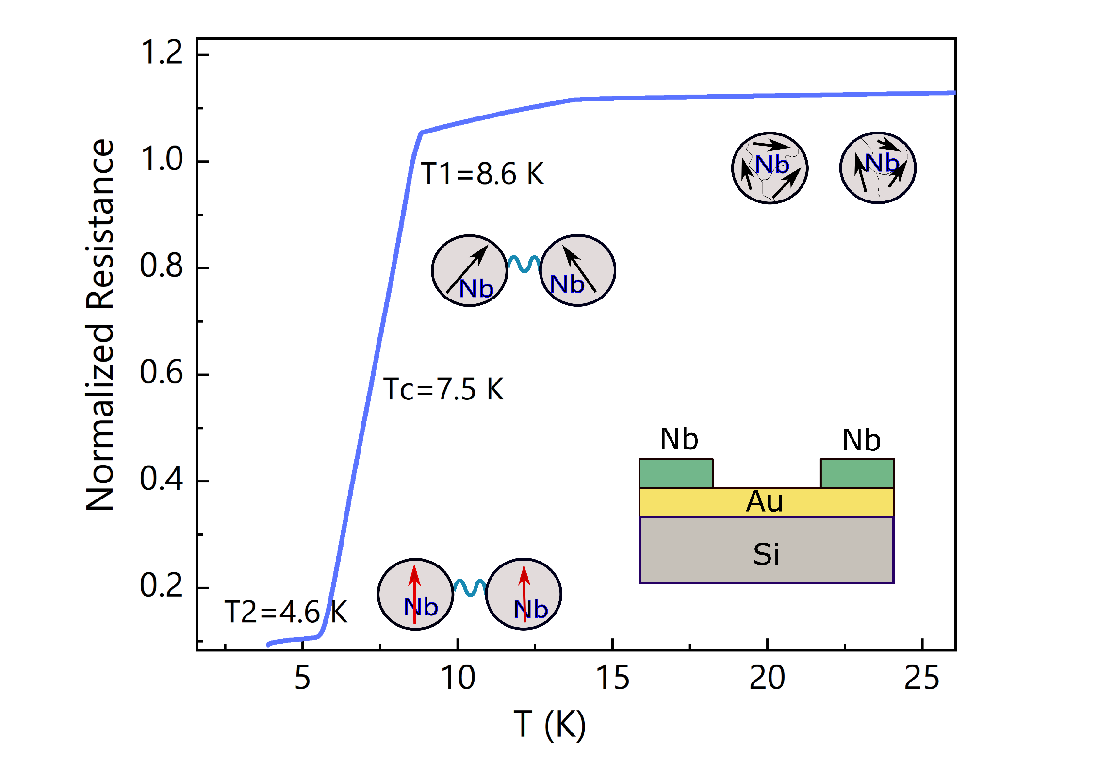
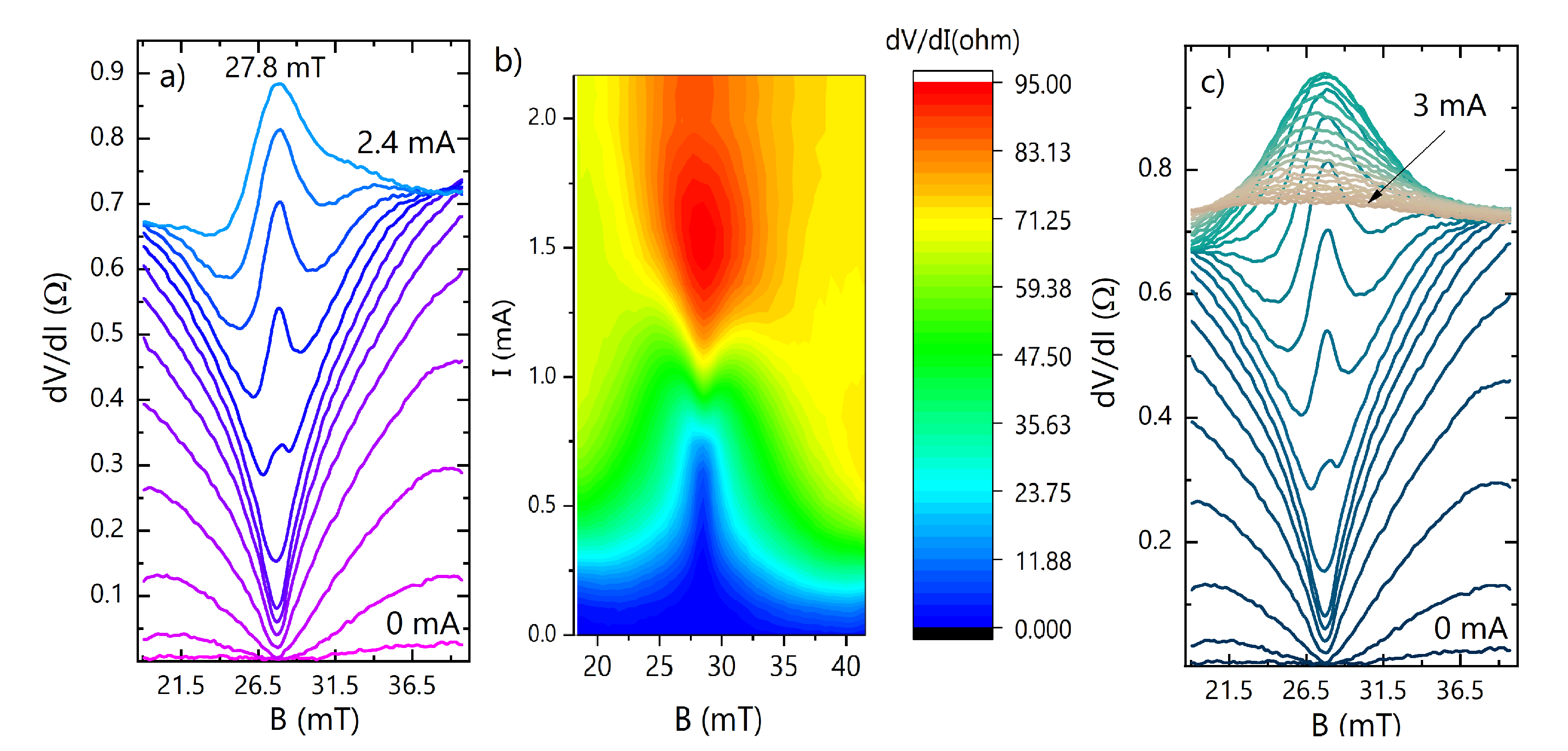
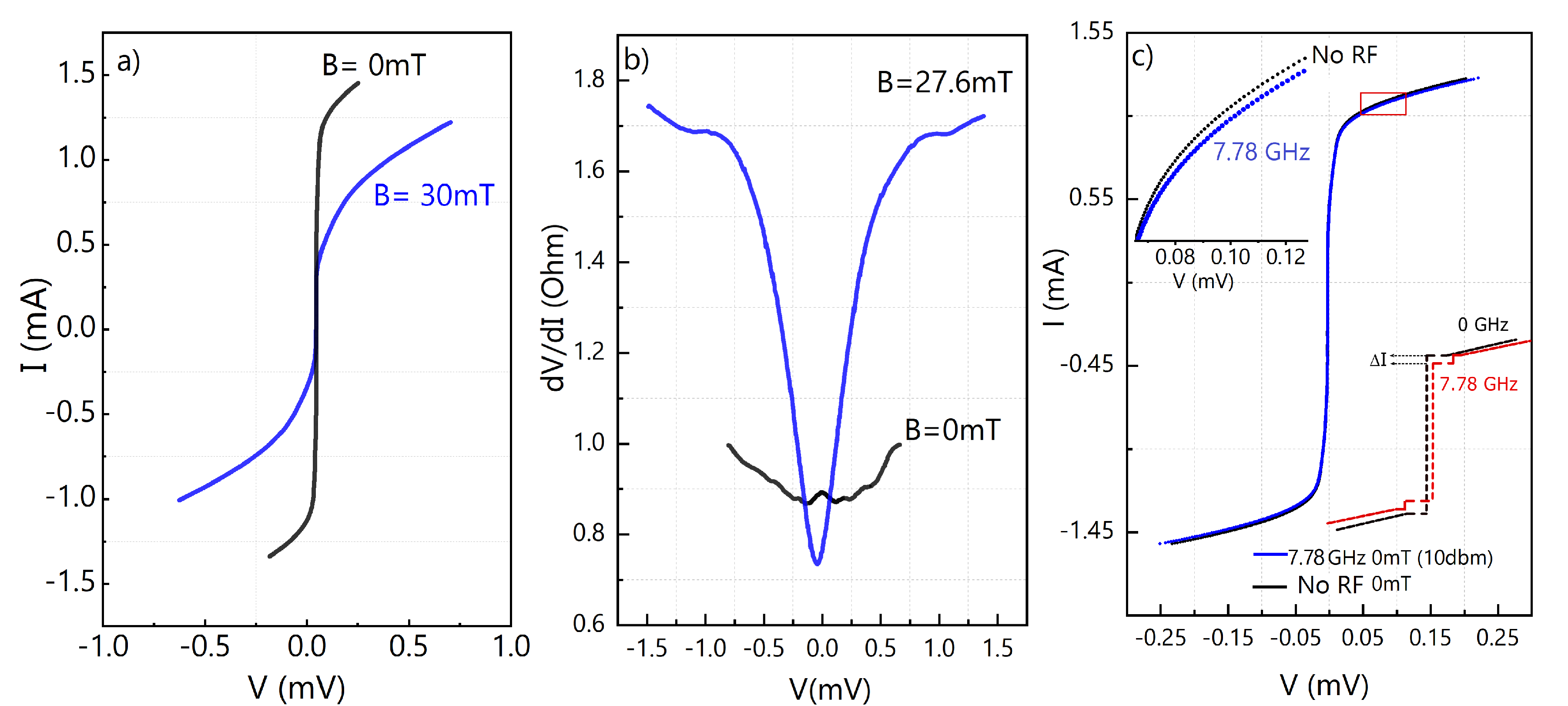
3. Results and Discussion
4. Conclusions
Author Contributions
Funding
Acknowledgments
Conflicts of Interest
References
- Dhillon, S.S.; Vitiello, M.S.; Linfield, E.H.; Davies, A.G.; Hoffmann, M.C.; Booske, J.; Paoloni, C.; Gensch, M.; Weightman, P.; Williams, G.P.; et al. The 2017 terahertz science and technology roadmap. J. Phys. D. Appl. Phys. 2017, 50. [Google Scholar] [CrossRef]
- Ortolani, M.; Lupi, S.; Baldassarre, L.; Schade, U.; Calvani, P.; Takano, Y.; Nagao, M.; Takenouchi, T.; Kawarada, H. Low-Energy Electrodynamics of Superconducting Diamond. Phys. Rev. Lett. 2006, 97, 097002. [Google Scholar] [CrossRef] [PubMed] [Green Version]
- Nanni, E.A.; Huang, W.R.; Hong, K.H.; Ravi, K.; Fallahi, A.; Moriena, G.; Dwayne Miller, R.J.; Kärtner, F.X. Terahertz-driven linear electron acceleration. Nat. Commun. 2015, 6, 8486. [Google Scholar] [CrossRef] [PubMed]
- Jepsen, P.; Cooke, D.; Koch, M. Terahertz spectroscopy and imaging - Modern techniques and applications. Laser Photon. Rev. 2011, 5, 124–166. [Google Scholar] [CrossRef]
- Saeedkia, D. Handbook of Terahertz Technology for Imaging, Sensing and Communications; Woodhead Publishing: Sawston, UK, 2013. [Google Scholar]
- Karasik, B.S.; Sergeev, A.V.; Prober, D.E. Nanobolometers for THz Photon Detection. IEEE Trans. Terahertz Sci. Technol. 2011, 1, 97–111. [Google Scholar] [CrossRef] [Green Version]
- Rezvani, S.; Perali, A.; Fretto, M.; De Leo, N.; Flammia, L.; Milošević, M.; Nannarone, S.; Pinto, N. Substrate-Induced Proximity Effect in Superconducting Niobium Nanofilms. Conden. Matter 2018, 4, 1. [Google Scholar] [CrossRef] [Green Version]
- Toma, A.; Tuccio, S.; Prato, M.; De Donato, F.; Perucchi, A.; Di Pietro, P.; Marras, S.; Liberale, C.; Proietti Zaccaria, R.; De Angelis, F.; et al. Squeezing Terahertz Light into Nanovolumes: Nanoantenna Enhanced Terahertz Spectroscopy (NETS) of Semiconductor Quantum Dots. Nano Lett. 2015, 15, 386–391. [Google Scholar] [CrossRef]
- D’Apuzzo, F.; Piacenti, A.R.; Giorgianni, F.; Autore, M.; Guidi, M.C.; Marcelli, A.; Schade, U.; Ito, Y.; Chen, M.; Lupi, S. Terahertz and mid-infrared plasmons in three-dimensional nanoporous graphene. Nat. Commun. 2017, 8, 14885. [Google Scholar] [CrossRef]
- Richards, P.L. Bolometers for infrared and millimeter waves. J. Appl. Phys. 1994, 76, 1–24. [Google Scholar] [CrossRef] [Green Version]
- Ozyuzer, L.; Koshelev, A.E.; Kurter, C.; Gopalsami, N.; Li, Q.; Tachiki, M.; Kadowaki, K.; Yamamoto, T.; Minami, H.; Yamaguchi, H.; et al. Emission of Coherent THz Radiation from Superconductors. Science 2007, 318, 1291–1293. [Google Scholar] [CrossRef] [Green Version]
- Du, J.; Smart, K.; Li, L.; Leslie, K.E.; Hanham, S.M.; Wang, D.H.C.; Foley, C.P.; Ji, F.; Li, X.D.; Zeng, D.Z. A cryogen-free HTS Josephson junction detector for terahertz imaging. Supercond. Sci. Technol. 2015, 28, 084001. [Google Scholar] [CrossRef] [Green Version]
- Hammar, A.; Cherednichenko, S.; Bevilacqua, S.; Drakinskiy, V.; Stake, J. Terahertz Direct Detection in YBa2Cu3O Microbolometers. IEEE Trans. Terahertz Sci. Technol. 2011, 1, 390–394. [Google Scholar] [CrossRef] [Green Version]
- Seliverstov, S.; Maslennikov, S.; Ryabchun, S.; Finkel, M.; Klapwijk, T.M.; Kaurova, N.; Vachtomin, Y.; Smirnov, K.; Voronov, B.; Goltsman, G. Fast and sensitive terahertz direct detector based on superconducting antenna-coupled hot electron bolometer. IEEE Trans. Appl. Supercond. 2015. [Google Scholar] [CrossRef]
- Carturan, S.; Maggioni, G.; Rezvani, S.; Gunnella, R.; Pinto, N.; Gelain, M.; Napoli, D. Wet chemical treatments of high purity Ge crystals for γ-ray detectors: Surface structure, passivation capabilities and air stability. Mater. Chem. Phys. 2015, 161, 116–122. [Google Scholar] [CrossRef]
- Sartale, S.; Ansari, A.; Rezvani, S.J. Influence of Ti film thickness and oxidation temperature on TiO2 thin film formation via thermal oxidation of sputtered Ti film. Mater. Sci. Semicond. Proc. 2013, 16, 2005–2012. [Google Scholar] [CrossRef]
- Rezvani, S.J.; Pinto, N.; Boarino, L.; Celegato, F.; Favre, L.; Berbezier, I. Diffusion induced effects on geometry of Ge nanowires. Nanoscale 2014, 6, 7469–7473. [Google Scholar] [CrossRef] [Green Version]
- Rezvani, S.J.; Pinto, N.; Enrico, E.; D’Ortenzi, L.; Chiodoni, A.; Boarino, L. Thermally activated tunneling in porous silicon nanowires with embedded Si quantum dots. J. Phys. D Appl. Phys. 2016, 49, 105104. [Google Scholar] [CrossRef]
- Pinto, N.; Rezvani, S.J.; Favre, L.; Berbezier, I.; Fretto, M.; Boarino, L. Geometrically induced electron-electron interaction in semiconductor nanowires. Appl. Phys. Lett. 2016, 109, 123101. [Google Scholar] [CrossRef]
- Rezvani, S.; Pasqualini, M.; Witkowska, A.; Gunnella, R.; Birrozzi, A.; Minicucci, M.; Rajantie, H.; Copley, M.; Nobili, F.; Di Cicco, A. Binder-induced surface structure evolution effects on Li-ion battery performance. Appl. Surface Sci. 2018, 435, 1029–1036. [Google Scholar] [CrossRef]
- Luukanen, A.; Hadfield, R.H.; Miller, A.J.; Grossman, E.N. A superconducting antenna-coupled microbolometer for THz applications. In Proceedings of the Terahertz for Military and Security Applications II, Orlando, FL, USA, 8 September 2004. [Google Scholar]
- Ariyoshi, S.; Otani, C.; Dobroiu, A.; Sato, H.; Kawase, K.; Shimizu, H.M.; Taino, T.; Matsuo, H. Terahertz imaging with a direct detector based on superconducting tunnel junctions. Appl. Phys. Lett. 2006, 88, 203503. [Google Scholar] [CrossRef]
- Kislinskii, Y.; Constantinian, K.; Borisenko, I.; Ovsyannikov, G.; Yagoubov, P. Submillimeter wave signal detection by bicrystal YBCO Josephson junctions at liquid nitrogen temperatures. Physica C 2002, 372–376, 436–439. [Google Scholar] [CrossRef]
- Resnick, D.J.; Garland, J.C.; Boyd, J.T.; Shoemaker, S.; Newrock, R.S. Kosterlitz-Thouless Transition in Proximity-Coupled Superconducting Arrays. Phys. Rev. Lett. 1981, 47, 1542–1545. [Google Scholar] [CrossRef]
- Abraham, D.W.; Lobb, C.J.; Tinkham, M.; Klapwijk, T.M. Resistive transition in two-dimensional arrays of superconducting weak links. Phys. Rev. B 1982, 26, 5268–5271. [Google Scholar] [CrossRef]
- Pinto, N.; Rezvani, S.J.; Perali, A.; Flammia, L.; Milošević, M.V.; Fretto, M.; Cassiago, C.; De Leo, N. Dimensional crossover and incipient quantum size effects in superconducting niobium nanofilms. Sci. Rep. 2018, 8, 4710. [Google Scholar] [CrossRef] [Green Version]
- Baturina, T.I.; Vinokur, V.M.; Mironov, A.Y.; Chtchelkatchev, N.M.; Nasimov, D.A.; Latyshev, A.V. Nanopattern-stimulated superconductor-insulator transition in thin TiN films. EPL 2011, 93, 47002. [Google Scholar] [CrossRef]
- Rezvani, J.; Di Gioacchino, D.; Gatti, C.; Poccia, N.; Ligi, C.; Tocci, S.; Cestelli Guidi, M.; Cibella, S.; Lupi, S.; Marcelli, A. Tunable Vortex Dynamics in Proximity Junction Arrays: A Possible Accurate and Sensitive 2D THz Detector. Acta Phys. Polonica A 2020, 137, 17–20. [Google Scholar] [CrossRef]
- Poccia, N.; Baturina, T.I.; Coneri, F.; Molenaar, C.G.; Wang, X.R.; Bianconi, G.; Brinkman, A.; Hilgenkamp, H.; Golubov, A.A.; Vinokur, V.M. Critical behavior at a dynamic vortex insulator-to-metal transition. Science 2015, 349, 1202–1205. [Google Scholar] [CrossRef]
- Benz, S.P.; Rzchowski, M.S.; Tinkham, M.; Lobb, C.J. Critical currents in frustrated two-dimensional Josephson arrays. Phys. Rev. B 1990, 42, 6165–6171. [Google Scholar] [CrossRef]
- Argaman, N. Nonequilibrium Josephson-like effects in wide mesoscopic SNS junctions. Superlattices Microstruct. 1999, 25, 861–875. [Google Scholar] [CrossRef] [Green Version]
- Zitzmann, J.; Ustinov, A.V.; Levitchev, M.; Sakai, S. Super-relativistic fluxon in a Josephson multilayer: Experiment and simulation. Phys. Rev. B 2002, 66, 064527. [Google Scholar] [CrossRef]
- Sakai, S.; Bodin, P.; Pedersen, N.F. Fluxons in thin-film superconductor-insulator superlattices. J. Appl. Phys. 1993, 73, 2411–2418. [Google Scholar] [CrossRef] [Green Version]
- Goldobin, E.; Wallraff, A.; Thyssen, N.; Ustinov, A. Cherenkov radiation in coupled long Josephson junctions. Phys. Rev. B 1998, 57. [Google Scholar] [CrossRef] [Green Version]
- Tran, V.H.; Zaleski, T.A.; Bukowski, Z.; Tran, L.M.; Zaleski, A.J. Tuning superconductivity in Eu(Fe0.81Co0.19)2As2 with magnetic fields. Phys. Rev. B 2012, 85, 052502. [Google Scholar] [CrossRef]
- Schöndorf, M.; Govia, L.C.G.; Vavilov, M.G.; McDermott, R.; Wilhelm, F.K. Optimizing microwave photodetection: Input–output theory. Quantum Sci. Technol. 2018, 3, 024009. [Google Scholar] [CrossRef] [Green Version]
- Shapiro, S. Josephson Currents in Superconducting Tunneling: The Effect of Microwaves and Other Observations. Phys. Rev. Lett. 1963, 11, 80–82. [Google Scholar] [CrossRef]
- Tachiki, M.; Koyama, T.; Takahashi, S. Electromagnetic phenomena related to a low-frequency plasma in cuprate superconductors. Phys. Rev. B 1994, 50, 7065–7084. [Google Scholar] [CrossRef] [PubMed]
- Barone, A.; Paternò, G. Physics and Applications of the Josephson Effect; Wiley: New York, NY, USA, 1982. [Google Scholar] [CrossRef]
- Jeon, Y.; Jung, S.; Jin, H.; Mo, K.; Kim, K.R.; Park, W.K.; Han, S.T.; Park, K. Highly-Sensitive Thin Film THz Detector Based on Edge Metal-Semiconductor-Metal Junction. Sci. Rep. 2017, 7, 16830. [Google Scholar] [CrossRef] [PubMed]
- Du, J.; Hellicar, A.D.; Li, L.; Hanham, S.M.; Nikolic, N.; Macfarlane, J.C.; Leslie, K.E. Terahertz imaging using a high-Tcsuperconducting Josephson junction detector. Supercond. Sci. Technol. 2008, 21, 125025. [Google Scholar] [CrossRef]
© 2020 by the authors. Licensee MDPI, Basel, Switzerland. This article is an open access article distributed under the terms and conditions of the Creative Commons Attribution (CC BY) license (http://creativecommons.org/licenses/by/4.0/).
Share and Cite
Rezvani, S.J.; Gioacchino, D.D.; Gatti, C.; Ligi, C.; Guidi, M.C.; Cibella, S.; Fretto, M.; Poccia, N.; Lupi, S.; Marcelli, A. Proximity Array Device: A Novel Photon Detector Working in Long Wavelengths. Condens. Matter 2020, 5, 33. https://doi.org/10.3390/condmat5020033
Rezvani SJ, Gioacchino DD, Gatti C, Ligi C, Guidi MC, Cibella S, Fretto M, Poccia N, Lupi S, Marcelli A. Proximity Array Device: A Novel Photon Detector Working in Long Wavelengths. Condensed Matter. 2020; 5(2):33. https://doi.org/10.3390/condmat5020033
Chicago/Turabian StyleRezvani, S. Javad, Daniele Di Gioacchino, Claudio Gatti, Carlo Ligi, Mariangela Cestelli Guidi, Sara Cibella, Matteo Fretto, Nicola Poccia, Stefano Lupi, and Augusto Marcelli. 2020. "Proximity Array Device: A Novel Photon Detector Working in Long Wavelengths" Condensed Matter 5, no. 2: 33. https://doi.org/10.3390/condmat5020033
APA StyleRezvani, S. J., Gioacchino, D. D., Gatti, C., Ligi, C., Guidi, M. C., Cibella, S., Fretto, M., Poccia, N., Lupi, S., & Marcelli, A. (2020). Proximity Array Device: A Novel Photon Detector Working in Long Wavelengths. Condensed Matter, 5(2), 33. https://doi.org/10.3390/condmat5020033