Article

Classifying Induced Superconductivity in Atomically Thin Dirac-Cone Materials

by
Evgueni F. Talantsev
1,2
1
M. N. Miheev Institute of Metal Physics, Ural Branch, Russian Academy of Sciences, 18, S. Kovalevskoy St., Ekaterinburg 620108, Russia
2
NANOTECH Centre, Ural Federal University, 19 Mira St., Ekaterinburg 620002, Russia
Condens. Matter 2019, 4(3), 83; https://doi.org/10.3390/condmat4030083
Submission received: 19 August 2019 / Revised: 15 September 2019 / Accepted: 16 September 2019 / Published: 18 September 2019
(This article belongs to the Special Issue From cuprates to Room Temperature Superconductors)

Abstract

:
Recently, Kayyalha et al. (Phys. Rev. Lett., 2019, 122, 047003) reported on the anomalous enhancement of the self-field critical currents (Ic(sf,T)) at low temperatures in Nb/BiSbTeSe2-nanoribbon/Nb Josephson junctions. The enhancement was attributed to the low-energy Andreev-bound states arising from the winding of the electronic wave function around the circumference of the topological insulator BiSbTeSe2 nanoribbon. It should be noted that identical enhancement in Ic(sf,T) and in the upper critical field (Bc2(T)) in approximately the same reduced temperatures, were reported by several research groups in atomically thin junctions based on a variety of Dirac-cone materials (DCM) earlier. The analysis shows that in all these S/DCM/S systems, the enhancement is due to a new superconducting band opening. Taking into account that several intrinsic superconductors also exhibit the effect of new superconducting band(s) opening when sample thickness becomes thinner than the out-of-plane coherence length (ξc(0)), we reaffirm our previous proposal that there is a new phenomenon of additional superconducting band(s) opening in atomically thin films.

1. Introduction

Intrinsic superconductors can be grouped into 32 classes under “conventional”, “possibly unconventional”, and “unconventional” categories, according to the mechanism believed to give rise to superconductivity [1]. One of the most widely used concepts to represent all 32 classes of superconductors was proposed by Uemura et al. [2,3]. The concept of the Uemura plot is based on the utilization of two fundamental temperatures of superconductors: one is the Fermi temperature (TF) (X-axis), and the superconducting transition temperature (Tc) (Y-axis). In the most recently updated Uemura plot (Figure 1), it can be seen that elemental superconductors are located for wide range of Tc/TF ≤ 0.001, while all unconventional superconductors, including both nearly-room-temperature superconductors of H3S [4] and LaH10 [5] (for which experimentally measured upper critical field data [6,7] was analyzed in Refs. [8,9]), are located within a narrow band of 0.01 ≤ Tc/TF ≤ 0.05.
It should be mentioned that Hardy et al. [10] in 1993 (seven years after the discovery of high-temperature superconductivity in cuprates by Bednoltz and Mueller [11]) were the first to experimentally find that YBa2Cu2O7-x has nodal superconducting gap. This experimental result was used to propose d-wave superconducting gap symmetry in HTS cuprates by Won and Maki [12]. It should be noted that several researchers and research groups (over last 33 years) have proposed different mechanisms for high-temperature superconductivity in cuprates, the first two-band BCS superconductor (MgB2), pnictides, and hydrogen-rich superconductors, for which we refer the reader to original papers and comprehensive reviews [13,14,15,16,17,18,19,20,21,22,23,24,25,26,27,28,29,30,31].
Despite some differences, all intrinsic superconductors can induce superconducting state in non-superconducting materials via the Holm-Meissner effect [36] (also designated as the proximity effect [37,38]). As direct consequence of this, non-dissipative transport current can flow throw the non-superconducting material at superconductor/non-superconductor/superconductor (S/N/S) junctions. The amplitude of this non-dissipative transport current at self-field conditions (when no external magnetic field is applied) (Ic (sf,T)) was given by Ambegaokar and Baratoff (AB) [39,40]:
I c ( s f , T ) = π Δ ( T ) 2 e R n t a n h ( Δ ( T ) 2 k B T ) ,
where Δ(T) is the temperature-dependent superconducting gap, e is the electron charge, normal-state tunneling resistance (Rn) is the normal-state tunneling resistance in the junction, and kB is the Boltzmann constant.
Many interesting physical effects are expected if the non-superconducting part of the S/N/S junction is made of single-layer graphene (SLG) [41]; multiple-layer graphene (MLG) [42]; graphene-like materials [43]; and many other new 2D- and nano-DCMs, which are under on-going discovery/invention/exploration [44,45,46,47,48,49,50,51,52,53,54,55,56,57,58,59,60,61,62,63,64,65,66,67,68,69,70,71,72,73]. One interesting class of S/N/S junctions is the non-superconducting part of the device made of topological insulators (TI) [74,75,76,77,78,79,80,81]. Temperature-dependent self-field critical currents (Ic(sf,T)) in this class of junctions were first reported by Veldhorst et al. in Nb/Bi2Te3/Nb [52], and later by Kurter et al. in Nb/Bi2Se3/Nb [53], by Charpentier et al. in Al/Bi2Te3/Al [76], and by other research groups in different systems (extended reference list for studied S/TI/S junctions can be found in Refs. [79,80]).
Recently, Kayyalha et al. [82] have reported on anomalous enhancement of Ic(sf,T) at the Nb/BiSbTeSe2-nanoribon/Nb junction at temperatures of T ≤ 0.25Tc. They confirmed the effect in all five studied junctions [82], for which TI parts were made of BiSbTeSe2 flakes with thicknesses of 2b, which varied from 30 nm to 50 nm, and flakes widths of 2a, which varied from 266 nm to 390 nm. It should be noted that in all these S/TI/S junctions, BiSbTeSe2-nanoribbons thicknesses and widths were smaller than the ground state superconducting coherence length (2b << 2a < ξ(0) ~ 600 nm) in these devices [82]. For one junction, made of wider BiSbTeSe2-nanoribon (2a = 4 μm (Figure S4 of Supplementary Information of Ref. [82])), measurements were performed only at low temperatures (T < 2 K, which is about T < 0.2Tc (taking into account that Nb has Tc = 8.9–9.6 K [83])), and thus more experimental studies are required for this 4-μm wide Nb/BiSbTeSe2-nanoribon/Nb junction to see the Ic(sf,T) enhancement.
It needs to be stressed that identical Ic(sf,T) enhancement (or, in another words, Ic(sf,T) upturn [46]) at approximately the same reduced temperature of T ≤ 0.25Tc in atomically-thin S/N/S junction was first reported by Calado et al. [46] in MoRe/SLG/MoRe junction in 2015. One year later, less prominent Ic(sf,T) enhancement (which wass, however, still very clearly visible in raw experimental data [84]) in nominally the same MoRe/SLG/MoRe junctions at T ≤ 0.25Tc was reported by Borzenets et al. [49]. Based on this, it would be incorrect to attribute the Ic(sf,T) enhancement at low reduced temperatures in Nb/BiSbTeSe2-nanoribon/Nb [82] to unique property of S/TI/S junctions.
In addition, it is important to mention that Kurter et al. [53] were the first to report Ic(sf,T) enhancement at the S/TI/S junction at a reduced temperature of T ≤ 0.25Tc. At Nb/Bi2Se3/Nb junctions, Bi2Se3 flake had a thickness of 2b = 9 nm, and, thus, the condition of 2b < ξc(0) was also satisfied.
Overall, both S/TI/S [53,82], as S/SLG/S [46,49], studied junctions, for which the effect of the low-temperature Ic(sf,T) enhancement was observed to have non-superconducting parts thinner than the ground state out-of-plane coherence lengths, ξc(0). SLG thickness is 2b = 0.4–1.7 nm [84], and thus the condition of 2b << ξc(0) satisfies any SLG-based junctions.
It should be noted that several intrinsic superconductors exhibit multiple-band superconducting gapping [85,86] and the enhancement of the transition temperature [87,88,89,90,91,92,93] when the condition of 2b < ξc(0) [86] is satisfied. The first discovered material in this class of superconductors is atomically thin FeSe [88,89,90], in which a 13-fold increase (i.e., 100 K vs 7.5 K) is experimentally registered. Another milestone experimental finding in this field was reported by Liao et al. [43], who observed the effect of new superconducting band opening and Tc enhancement in few layers of stanene (which is the closest counterpart of graphene) by tuning the films’ thicknesses. To date, maximal Tc increase due to the effect [86] stands with another single-atomic layer superconductor, Td-MoTe2, for which Rhodes et al. [93] reported a 30-fold Tc increase when samples were thinneed down to a single atomic layer.
This paper reports the results of an analysis of Ic(sf,T) in Nb/BiSbTeSe2-nanoribbon/Nb [82] and Nb/(Bi0.06Sb0.94)2Te3/Nb [94] junctions, and of the upper critical field (Bc2(T)) in Sn/single-layer graphene (SLG)/Sn junctions [95]. In the results, it is shown that a new superconducting band opening phenomenon in atomically thin superconductors, which we proposed earlier [85,86], has further experimental support.

2. Models Description

In [85], it was proposed to substitute Δ(T) in Equation (1) by analytical expression given by Gross et al. [96], as follows:
Δ ( T ) = Δ ( 0 ) tanh ( π k B T c Δ ( 0 ) η ( Δ C C ) ( T c T 1 ) ) ,
where Δ(0) is the ground-state amplitude of the superconducting band, ΔC/C is the relative jump in electronic specific heat at the Tc, and η = 2/3 for s-wave superconductors [96]. In result, Tc, ΔC/C, Δ(0), and Rn of the S/N/S junction can be deduced by fitting experimental of an Ic(sf,T) dataset to Equation (1) (full expression for Equation (1) is given in Ref. [85]).
In [85], it was shown that S/SLG/S and S/Bi2Se3/S junctions exhibit two-decoupled band superconducting state, for which, for general case of multiple-decoupled bands, Ic(sf,T) can be described by the following equation:
I c ( s f , T ) = i = 1 N π Δ i ( T ) 2 e R n , i θ ( T c , i T ) t a n h ( Δ i ( T ) 2 k B T ) ,
where the subscript i refers to the i-band, θ(x) is the Heaviside step function, and each band has its own independent parameters of Tc,i, ΔCi/Ci, Δi(0), and Rn,i.
It should be noted that multiple-band induced superconductivity in junctions should be detectable by any technique which is sensitive to additional bands crossing the Fermi surface, for instance multiple distinct gaps should be evident in the temperature-dependence of the upper critical field, Bc2(T), for which general equation is:
B c 2 ( T ) = i = 1 N B c 2 , i ( T ) θ ( T c , i T ) ,
where, within each i-band, the upper critical field can be described by known model. In this paper, four Bc2(T) models were used to show that main result is model-independent. For instance, the following was used:
  • Two-fluid Gorter-Casimir (GC) model [97,98], as follows:
    B c 2 ( T ) = i = 1 N [ B c 2 , i ( 0 ) ( 1 ( T T c , i ) 2 ) θ ( T c , i T ) ] = ϕ 0 2 π i = 1 N [ θ ( T c , i T ) ξ i 2 ( 0 ) ( 1 ( T T c , i ) 2 ) ] ,
    where φ0 = 2.06810−15 Wb is flux quantum and ξi (0) is the ground state in-plane coherence length of the i--band. This model is widely used for single-band superconductors ranging from 3D near-room-temperature superconducting hydrides [4,7,8,9,99,100] to 2D superconductors [88,89,95,101].
  • Jones-Hulm-Chandrasekhar (JHC) model [102], as follows:
    B c 2 ( T ) = ϕ 0 2 π i = 1 N θ ( T c , i T ) ξ i 2 ( 0 ) ( 1 ( T T c , i ) 2 1 + ( T T c , i ) 2 ) ,
  • Werthamer-Helfand-Hohenberg model [103,104], for which we use analytical expression given by Baumgartner et al. [105] (we will designate this model as B-WHH herein), as follows:
    B c 2 ( T ) = ϕ 0 2 π i = 1 N θ ( T c , i T ) ξ i 2 ( 0 ) ( ( 1 T T c , i ) 0.153 ( 1 T T c , i ) 2 0.152 ( 1 T T c , i ) 4 0.693 ) ,
  • Gor’kov model [106], for which simple analytical expression was given by Jones et al. [102], as follows:
    B c 2 ( T ) = ϕ 0 2 π i = 1 N θ ( T c , i T ) ξ i 2 ( 0 ) ( ( 1.77 0.43 ( T T c , i ) 2 + 0.07 ( T T c , i ) 4 1.77 ) [ 1 ( T T c , i ) 2 ] ) ,

3. Results

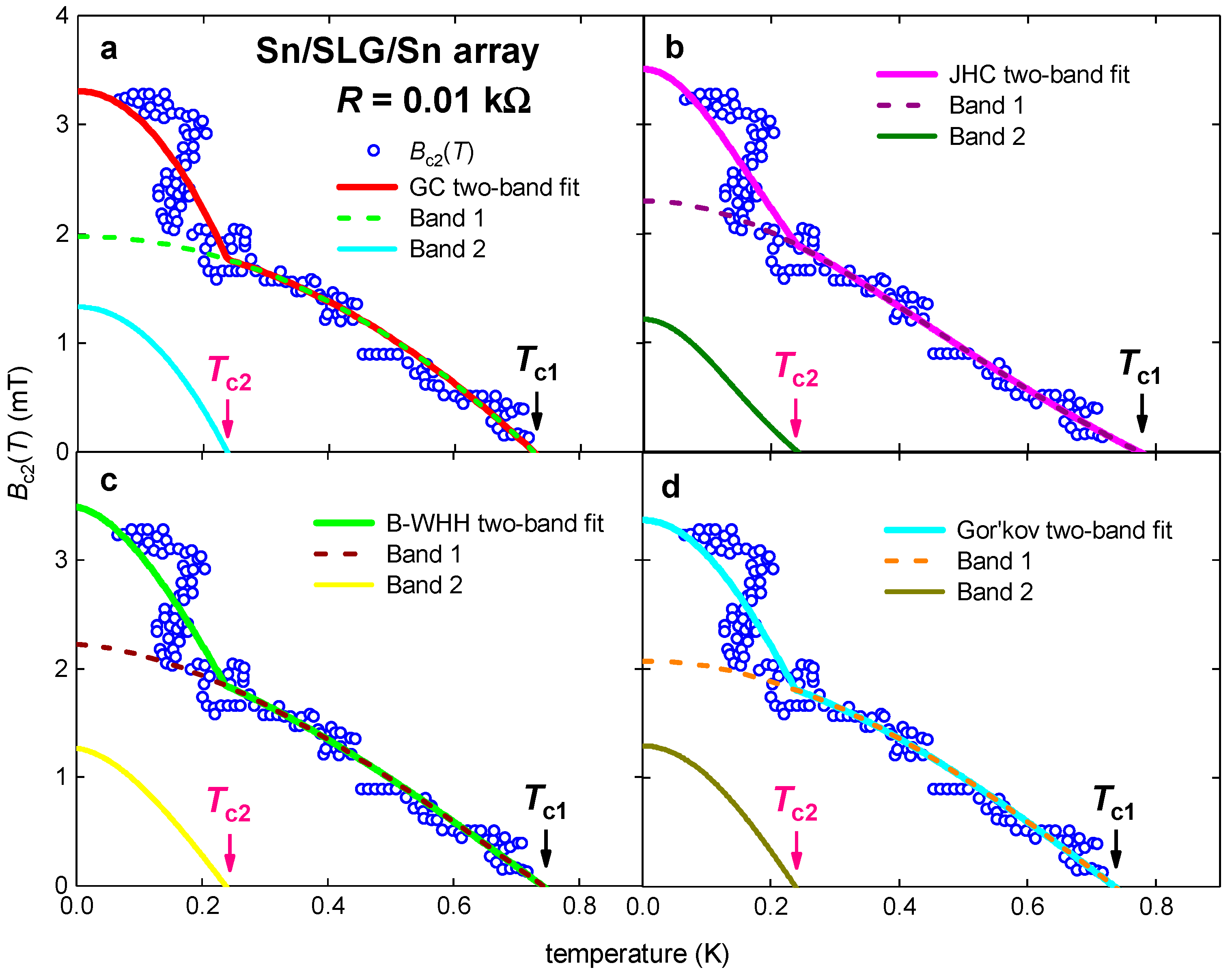
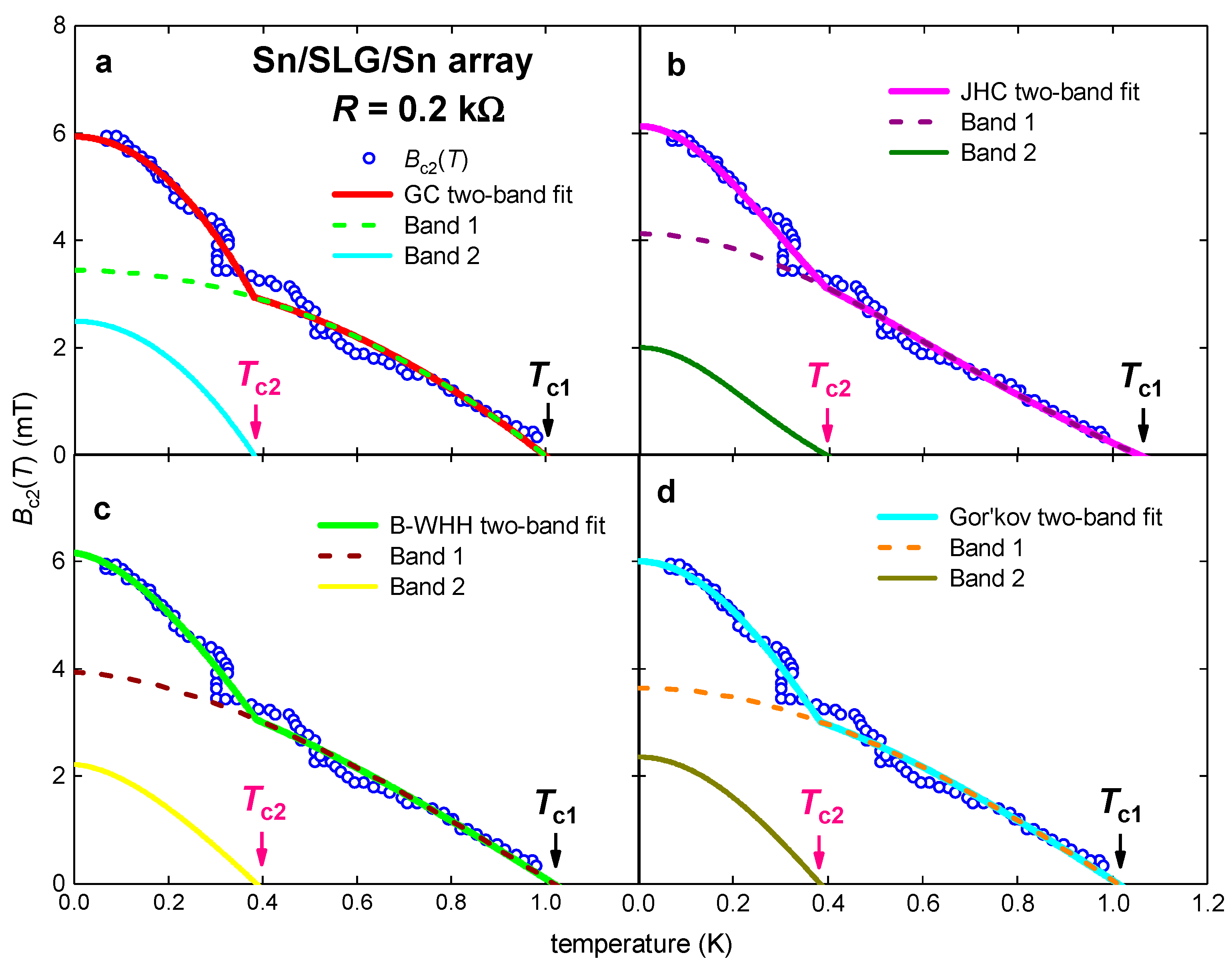
3.1. Planar Sn/SLG/Sn Array

Superconductivity in planar graphene junctions varies by the change of the charge carrier density when it moves away from the Dirac point in the dispersion [46,47,51]. This change is usually controlled by the gate voltage (Vg) that applies to the junction. Han et al. [95] reported on a proximity-coupled array of Sn discs with diameter of 400 nm on SLG that were placed in a hexagonal lattice separated by 1 μm between disks centers.
In Figure 2 and Figure 3, we show reported Bc2(T) for Sn/SLG/Sn array by Han et al. [95] in their Figure 4 and Figure 5 at gate voltage of Vg = 30 V. We defined Bc2(T) by two criteria of R = 0.01 kΩ (Figure 2) and R = 0.2 kΩ (Figure 3). It can be seen that there is an obvious upturn in Bc2(T) at T ≤ 0.4Tc, independent of the upper critical field definition criterion. It should be noted that the upturn occurs at practically the same reduced temperature at which Borzenets et al. [49] observed the Ic(sf,T) enhancement in MoRe/SLG/MoRe junctions.
Accordingly, these Bc2(T) datasets were fitted to four two-band models (Equations (5)–(8)); they are shown in Figure 2 and Figure 3. Deduced parameters, including the ratio of transition temperatures for two bands, T c 2 T c 1 = 0.32 ± 0.02 for R = 0.01 kΩ criterion (Figure 2), and T c 2 T c 1 = 0.38 ± 0.01 for R = 0.2 kΩ criterion (Figure 3), agreed with each other despite the fact that experimental Bc2(T) data were processed by four different models.
It should be noted that experimental data of Han et al. [95] show that there is a third upturn in Bc2(T) that can be seen at lowest experimentally available temperatures of T < 0.1 K and applied fields of about B ~ 4.5 mT in Figure 4 and Figure 5 [95], if the criterion of R ~ 0.05 kΩ (for the Bc2(T) definition) are applied.
Despite the fact that authors [61] did not mention the presence of these two upturns in raw experimental Bc2(T) data and more detailed measurements of Bc2(T) requires to reveal more accurately the position and parameters for the third band, there is already enough experimental evidence that Sn/SLG/Sn array exhibits at least two-superconducting bands gapping, and thus the report of Han et al. [61] supports the idea that atomically thin films exhibit multiple-band superconducting gapping phenomenon [85,86].

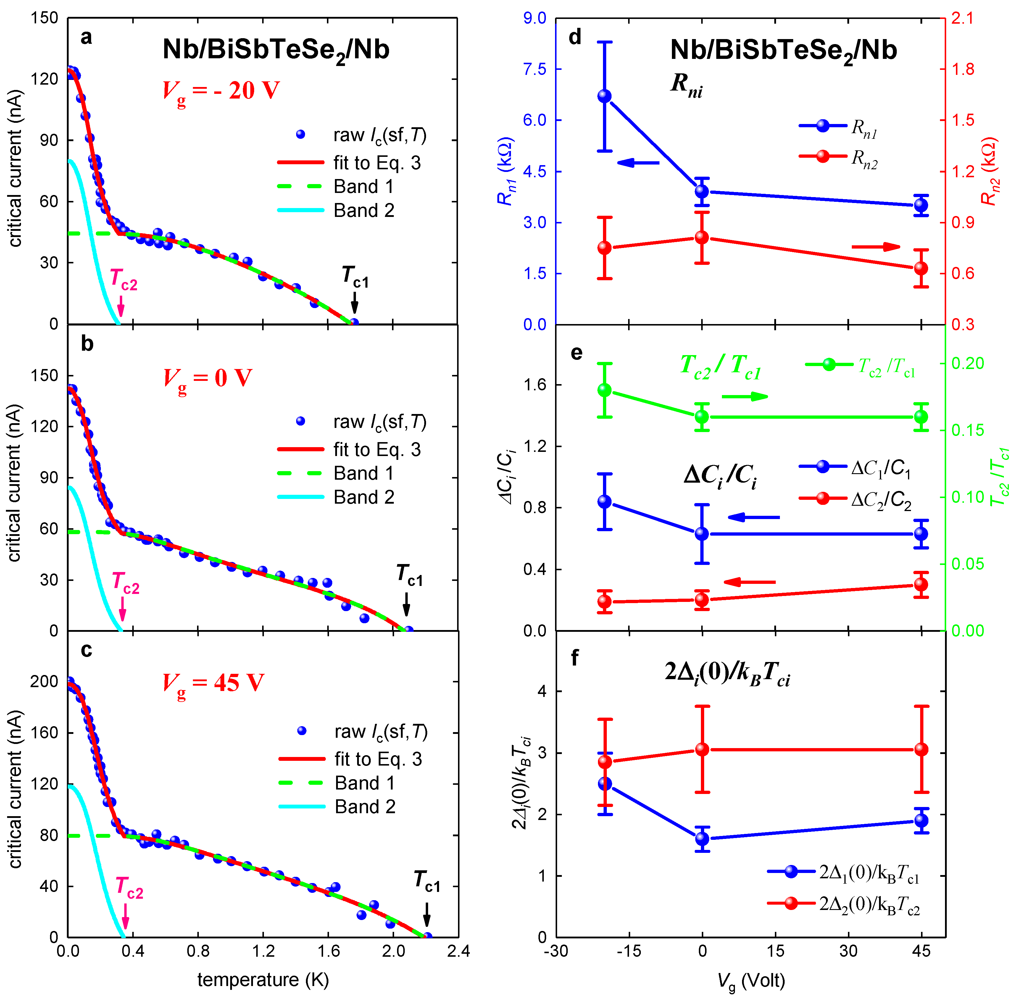
3.2. Planar Nb/BiSbTeSe2-Nanoribbon/Nb Junctions

Recently, Kayyalha et al. [82], in their Figure 2 and S1, reported Ic(sf,T) for five Nb/BiSbTeSe2-nanopribbon/Nb junctions at different Vgs. The thickness of BiSbTeSe2 flakes varied from 2b = 30 nm to 50 nm, and based on reported ξ(0) ~ 600 nm [82], the condition of 2b < ξ(0) [85,86] was satisfied for all junctions.

3.2.1. Nb/BiSbTeSe2-Nanoribbon/Nb Junctions

In Figure 4, we show experimental Ic(sf,T) datasets for Sample 1 [82] reported for three gate voltages: Vg = −20 V (Figure 4a), 0 V (Figure 4b), and +45 V (Figure 4c). Ic(sf,T) fits to Equation (3) were performed for all parameters to be free, as experimental raw datasets were rich enough to carry out these sorts of fits.
Deduced Rni, T c 1 T c 2 , ΔCi/Ci, Δi(0), and 2 Δ i ( 0 ) k B T c , i for both superconducting bands as functions of Vg are shown in Figure 4d–f).
It needs to be stressed that within the range of uncertainties, deduced Rn1 values are well agree with directly measured values by Kayyalha et al. [82] (these values are reported in Figure 1a of Ref. [82]). Increasingly often, measured raw Ic(sf,T) data, and especially at high reduced temperatures, are required to reduce the uncertainty for Rn1 values.
Most notable outcome of our analysis is that, within uncertainty ranges, fundamental superconducting parameters for both bands, including the ratio of T c 2 T c 1 , remain unchanged vs. gate voltage variation in the range from −20 V to 45 V. This means that two-band superconducting state in Nb/BiSbTeSe2-nanoribbon/Nb junction is very robust and mostly independent from the change in Vg. This is an unexpected result, because there is generally accepted view that because Vg is determined the electronic state in 2D-systems in the normal state, it should also determine the superconducting state. However, performed analysis shows that this is not a case in general. As was already mentioned, there is a need for more frequent measurements of raw Ic(sf,T) data, which will allow one to reduce uncertainties for all deduced parameters.

3.2.2. Nb/BiSbTeSe2-Nanoribbon/Nb Junction

In Figure 5a, we show experimental Ic(sf,T) dataset for Nb/BiSbTeSe2-nanoribbon/Nb (Sample 3) reported by Kayyalha et al. [82].
Raw experimental Ic(sf,T) dataset for this sample was not reach enough at T 0.6 , and thus we cannot perform the fit to Equation (3) for all parameters to be free. To run the model (Equation (3)), we make the same model restriction, as we did in our previous work [85]:
Δ C 1 C 1 = Δ C 2 C 2 = Δ C C ,
2 Δ 1 ( 0 ) k B T 1 = 2 Δ 2 ( 0 ) k B T 2 = 2 Δ ( 0 ) k B T c ,
i.e., we forced ΔCi/Ci and 2 Δ i ( 0 ) k B T c , i values to be the same for both bands. As a result, deduced Rni, Tci, T c 2 T c 1 ~ 1 4 , ΔC/C, Δi(0) and 2 Δ ( 0 ) k B T c for this junction are very close to ones deduced for Sample 1 (Figure 4).

3.3. Planar MoRe/SLG/MoRe Junction

To demonstrate that findings in regard of Nb/BiSbTeSe2-nanoribbon/Nb junctions are generic for a much wide range of atomically-thin DCM-based Josephson junctions, in Figure 5b we show raw Ic(sf,T) dataset and fit to the model (Equation (3)) for MoRe/SLG/MoRe reported by Calado et al. [46] for their Device A [46]. For the Ic(sf,T) fit for this device, we used the same parameters restrictions (Equations (9) and (10)), as for Nb/BiSbTeSe2-nanoribbon/Nb Sample 3 [82].
In work [85], this Ic(sf,T) dataset for MoRe/SLG/MoRe Device A [46] was already analyzed. What was found in this paper was that there is remarkable and practically undistinguishable similarity between reduced Ic(sf,T) datasets and fits for Nb/BiSbTeSe2-nanoribbon/Nb [48] and MoRe/SLG/MoRe [46] junctions (Figure 5). In an attempt to further extend atomically-thin S/DCM/S junctions, in next Section we analyze Ic(sf,T) data for Nb/(Bi0.06Sb0.94)2Te3-nanoribbon/Nb junction [94].

3.4. Planar Nb/(Bi0.06Sb0.94)2Te3-Nanoribbon/Nb Junction

In Figure 6, Ic(sf,T) in Nb/(Bi0.06Sb0.94)2Te3-nanoribbon/Nb reported by Schüffelgen et al. [94] are shown. TI nanoribbon has thickness of 2b = 10 nm, and, thus the condition of 2b < ξ(0) [85,86] is satisfied.
Due to the fact that the reported Ic(sf,T) dataset was not rich enough at high reduced temperatures, we restricted the model by utilizing Equations (9) and (10). Overall, fitted curves and all deduced parameters were very close to one reported by Borzenets et al. [49] for MoRe/SLG/MoRe junctions (which we processed and showed in our previous paper [85] in Figure 7).

4. Discussion

It should be noted that the idea of multiple-band superconductivity in bulk superconductors was proposed by Suhl et al. [107] in 1959, and it took more than forty years to discover the first two-band BCS superconductor (MgB2) [108] and about fifty years to discover multiple-band iron-based superconductors in 2006 [109]. Interband scattering in these materials have been discussed in details elsewhere [24,110,111,112].
It needs to be mentioned that Shalnikov discussed the discovery of the Tc increase in thin films [113], who reported the effect for lead and tin thin films more than eighty years ago. Three-fold increase in the transition temperature of thin granular Al films was reported three decades later by Cohen and Abeles [114], and the superconductivity in granular Al films is still active scientific topic [115,116]; the discussion of this effect in intrinsic superconductors, however, is beyond the scope of this paper.
It needs to be stressed that Calado et al. [46] in 2015 emphasized the necessity for a new model to explain the upturn in Ic(sf,T) registered in their MoRe/SLG/MoRe junction (Device A) at T ~ 1 4 T c (which we show in Figure 5b), because this Ic(sf,T) enhancement was not possible to explain using either the Eilenberger model (which is used to describe clean S/N/S junctions) [117] or the Usadel model (which describes diffusive S/N/S junctions) [118].
Our explanation for this upturn [85], which is well aligned with the Ic(sf,T) upturn in natural atomically thin superconductors [86], is that this Ic(sf,T) enhancement is due to a new superconducting band opening phenomenon when sample dimensions become smaller than some critical value. For this critical value, we proposed to use [86] the out-of-plane coherence length, ξc(0), which is still, after expanding our analysis herein, a good choice for the criterion.
It should be pointed out that this new opening band phenomenon does not necessarily cause the increase in observed transition temperature in comparison with “bulk” material. For instance, in pure Nb films [119], this new “thin film” band has lower transition temperature in comparison with “bulk” band [86]. In these circumstances, the researchers are not able to explore the further creation of devices or films for new superconducting band.
Thus, in many atomically thin films, which in fact exhibit a new band opening phenomenon, this effect has not been registered yet, because there is no guarantee that something important/interesting can be observed at low reduced temperatures, well below “bulk” or observed Tc for given atomically thin film.
It should be noted that the effect of new superconducting band opening [86] in atomically thin films can be detected using any experimental techniques that are sensitive to additional band(s) crossing the Fermi surface. To date, most evident confirmations for the phenomenon are related to the Ic(sf,T) upturn [43,85,86] and Bc2(T) upturn [43]; however, other techniques also should be able to detect this.
In this regard, the observation of the Ic(sf,T) upturn reported by Li et al. [78] in their Figure 4a at T = 2.5 K in Nb/Cd3As2-nanowire/Nb junction should be mentioned. However, raw experimental Ic(sf,T) dataset [78] was limited by measurements at T < 3.5 K, and thus we are not able to perform the analysis for this very interesting atomically-narrow S/TI/S junction at the moment.
There are very interesting results reported by Sasaki et al. [120] and by Andersen et al. [121], who found that temperature-dependent Bc2(T), in nanostructures of topological insulators, cannot be explained by single-band WHH model [103,104]. However, reported, to date, raw experimental Bc2(T) datasets [119,120] are insufficient to perform two-band model fit to reveal the presence of additional band at low reduced temperatures in these structures.
We also need to mention an interesting research field of interfaced superconductivity [71,122,123,124,125], where, as was proposed earlier, the enhancement of the superconductivity is also due to new superconducting band opening [86]. However, the discussion of this interesting field is beyond the scope of this paper.

5. Conclusions

In this paper, an analysis of recently reported experimental data on induced superconducting state in atomically thin Dirac-cone films was performed. It was shown that the phenomenon of the new superconducting band opening in atomically thin films [85,86], when the film thickness becomes thinner than the ground state out-of-plane coherence length, ξc(0), can be extended to an induced superconducting state in atomically thin DCM, as one was established before for natural superconductors, i.e., pure Nb, exfoliated 2H-TaS2, double-atomic layer FeSe, and a few layers of stanene [9].

Funding

This research was funded by the State Assignment of Minobrnauki of Russia, theme “Pressure” No. АААА-А18-118020190104-3, and by Act 211 Government of the Russian Federation, contract No. 02.A03.21.0006.

Acknowledgments

Author would like to thank Srijit Goswami and Lieven Vandersypen (Kavli Institute of Nanoscience, Delft University of Technology, The Netherlands) for providing raw self-field critical current data for the MoRe/SLG/MoRe devices analyzed in this work.

Conflicts of Interest

The funders had no role in the design of the study; in the collection, analyses, or interpretation of data; in the writing of the manuscript; or in the decision to publish the results.

References

  1. Hirsch, J.E.; Maple, M.B.; Marsiglio, F. Superconducting materials classes: Introduction and overview. Physica C 2015, 514, 1–8. [Google Scholar] [CrossRef] [Green Version]
  2. Uemura, Y.J.; Luke, G.M.; Sternlieb, B.J.; Brewer, J.H.; Carolan, J.F.; Hardy, W.N.; Kadono, R.; Kempton, J.R.; Kiefl, R.F.; Kreitzman, S.R. Universal correlations between Tc and n s m * (carrier density over effective mass) in high-Tc cuprate. Phys. Rev. Lett. 1989, 62, 2317–2320. [Google Scholar] [CrossRef] [PubMed]
  3. Uemura, Y.J. Condensation, excitation, pairing, and superfluid density in high-Tc superconductors: The magnetic resonance mode as a roton analogue and a possible spin-mediated pairing. J. Phys. Condens. Matter 2004, 16, S4515–S4540. [Google Scholar] [CrossRef]
  4. Drozdov, A.P.; Eremets, M.I.; Troyan, I.A.; Ksenofontov, V.; Shylin, S.I. Conventional superconductivity at 203 kelvin at high pressures in the sulfur hydride system. Nature 2015, 525, 73–76. [Google Scholar] [CrossRef] [PubMed]
  5. Somayazulu, M.; Ahart, M.; Mishra, A.K.; Geballe, Z.M.; Baldini, M.; Meng, Y.; Struzhkin, V.V.; Hemley, R.J. Evidence for superconductivity above 260 K in lanthanum superhydride at megabar pressures. Phys. Rev. Lett. 2019, 122, 027001. [Google Scholar] [CrossRef] [PubMed]
  6. Mozaffari, S.; Sun, D.; Minkov, V.S.; Drozdov, A.P.; Knyazev, D.; Betts, J.B.; Einaga, M.; Shimizu, K.; Eremets, M.I.; Balicas, L. Superconducting phase-diagram of H3S under high magnetic fields. Nat. Commun. 2019, 10, 2522. [Google Scholar] [CrossRef] [PubMed]
  7. Drozdov, A.P.; Kong, P.P.; Minkov, V.S.; Besedin, S.P.; Kuzovnikov, M.A.; Mozaffari, S.; Balicas, L.; Balakirev, F.F.; Graf, D.E.; Prakapenka, V.B. Superconductivity at 250 K in lanthanum hydride under high pressures. Nature 2019, 569, 528–531. [Google Scholar] [CrossRef] [PubMed] [Green Version]
  8. Talantsev, E.F. Classifying superconductivity in compressed H3S. Mod. Phys. Lett. B 2019, 33, 1950195. [Google Scholar] [CrossRef]
  9. Talantsev, E.F. Classifying hydrogen-rich superconductors. Mater. Res. Express 2019, 6, 106002. [Google Scholar] [CrossRef] [Green Version]
  10. Hardy, W.N.; Bonn, D.A.; Morgan, D.C.; Liang, R.; Zhang, K. Precision measurements of the temperature dependence of l in YBa2Cu3O6.95: Strong evidence for nodes in the gap function. Phys. Rev. Lett. 1993, 70, 3999–4002. [Google Scholar] [CrossRef]
  11. Bednorz, J.G.; Mueller, K.A. Possible high Tc superconductivity in the Ba-La-Cu-O system. Z. Phys. B 1986, 64, 189–193. [Google Scholar] [CrossRef]
  12. Won, H.; Maki, K. d-wave superconductor as a model of high-Tc superconductors. Phys. Rev. B 1994, 49, 1397–1402. [Google Scholar] [CrossRef] [PubMed]
  13. Hirsch, J.E. Hole superconductivity. Phys. Lett. A 1989, 134, 451–455. [Google Scholar] [CrossRef]
  14. Bianconi, A. On the possibility of new high Tc superconductors by producing metal heterostructures as in cuprate perovskites. Solid State Commun. 1994, 89, 933–936. [Google Scholar] [CrossRef]
  15. Bouquet, F.; Wang, Y.; Fisher, R.A.; Hinks, D.G.; Jorgensen, J.D.; Junod, A.; Phillips, N.E. Phenomenological two-gap model for the specific heat of MgB2. Europhys. Lett. 2001, 56, 856–862. [Google Scholar] [CrossRef]
  16. Bauer, E.; Paul, C.H.; Berger, S.T.; Majumdar, S.; Michor, H.; Giovannini, M.; Saccone, A.; Bianconi, A. Thermal conductivity of superconducting MgB2. J. Phys. Condens. Matter 2001, 13, L487–L494. [Google Scholar] [CrossRef]
  17. Carrington, A.; Manzano, F. Magnetic penetration depth of MgB2. Physica C 2003, 385, 205–214. [Google Scholar] [CrossRef]
  18. Agrestini, S.; Metallo, C.; Filippi, M.; Simonelli, L.; Campi, G.; Sanipoli, C.; Liarokapis, E.; De Negri, S.; Giovannini, M.; Saccone, A. Substitution of Sc for Mg in MgB2: Effects on transition temperature and Kohn anomaly. Phys. Rev. B 2004, 70, 134514. [Google Scholar] [CrossRef]
  19. Mazin, I.I.; Singh, D.J.; Johannes, M.D.; Du, M.H. Unconventional superconductivity with a sign reversal in the order parameter of LaFeAsO1−xFx. Phys. Rev. Lett. 2008, 101, 057003. [Google Scholar] [CrossRef]
  20. Kuroki, K.; Onari, S.; Arita, R.; Usui, H.; Tanaka, Y.; Kontani, H.; Aoki, H. Unconventional pairing originating from the disconnected Fermi surfaces of superconducting LaFeAsO1−xFx. Phys. Rev. Lett. 2008, 101, 087004. [Google Scholar] [CrossRef] [PubMed]
  21. Innocenti, D.; Caprara, S.; Poccia, N.; Ricci, A.; Valletta, A.; Bianconi, A. Shape resonance for the anisotropic superconducting gaps near a Lifshitz transition: The effect of electron hopping between layers. Supercond. Sci. Technol. 2011, 24, 015012. [Google Scholar] [CrossRef]
  22. Bianconi, A.; Innocenti, D.; Valletta, A.; Perali, A. Shape resonances in superconducting gaps in a 2DEG at oxide-oxide interface. J. Phys. Conf. Ser. 2014, 529, 012007. [Google Scholar] [CrossRef]
  23. Hosono, H.; Tanabe, K.; Takayama-Muromachi, E.; Kageyama, H.; Yamanaka, S.; Kumakura, H.; Nohara, M.; Hiramatsu, H.; Fujitsu, S. Exploration of new superconductors and functional materials, and fabrication of superconducting tapes and wires of iron pnictides. Sci. Technol. Adv. Mater. 2015, 16, 033503. [Google Scholar] [CrossRef] [PubMed]
  24. Hosono, H.; Kuroki, K. Iron-based superconductors: Current status of materials and pairing mechanism. Physica C 2015, 514, 399–422. [Google Scholar] [CrossRef] [Green Version]
  25. Bianconi, A.; Jarlborg, T. Superconductivity above the lowest Earth temperature in pressurized sulfur hydride. EPL (Europhys. Lett.) 2015, 112, 37001. [Google Scholar] [CrossRef] [Green Version]
  26. Hirsch, J.E.; Marsiglio, F. Hole superconductivity in H2S and other sulfides under high pressure. Physica C 2015, 511, 45–49. [Google Scholar] [CrossRef]
  27. Souza, T.X.R.; Marsiglio, F. Systematic study of the superconducting critical temperature in two- and three-dimensional tight-binding models: A possible scenario for superconducting H3S. Phys. Rev. B 2016, 94, 184509. [Google Scholar] [CrossRef]
  28. Harshman, D.R.; Fiory, A.T. Compressed H3S: Inter-sublattice Coulomb coupling in a high-Tc superconductor. J. Phys. Condens. Matter 2017, 29, 445702. [Google Scholar] [CrossRef]
  29. Bang, Y.; Stewart, G.R. Superconducting properties of the s±-wave state: Fe-based superconductors. J. Phys. Condens. Matter 2017, 29, 123003. [Google Scholar] [CrossRef]
  30. Kaplan, D.; Imry, Y. High-temperature superconductivity using a model of hydrogen bonds. Proc. Natl. Acad. Sci. USA 2018, 115, 5709–5713. [Google Scholar] [CrossRef] [Green Version]
  31. Moskvin, A.S.; Panov, Y.D. Topological structures in unconventional scenario for 2D cuprates. J. Supercond. Nov. Magn. 2019, 32, 61–84. [Google Scholar] [CrossRef]
  32. Ye, J.T.; Zhang, Y.J.; Akashi, R.; Bahramy, M.S.; Arita, R.; Iwasa, Y. Superconducting dome in a gate-tuned band insulator. Science 2012, 338, 1193–1196. [Google Scholar] [CrossRef] [PubMed]
  33. Qian, T.; Wang, X.-P.; Jin, W.-C.; Zhang, P.; Richard, P.; Xu, G.; Dai, X.; Fang, Z.; Guo, J.-G.; Chen, X.-L. Absence of a holelike Fermi surface for the iron-based K0.8Fe1.7Se2 superconductor revealed by angle-resolved photoemission spectroscopy. Phys. Rev. Lett. 2011, 106, 187001. [Google Scholar] [CrossRef] [PubMed]
  34. Hashimoto, K.; Cho, K.; Shibauchi, T.; Kasahara, S.; Mizukami, Y.; Katsumata, R.; Tsuruhara, Y.; Terashima, T.; Ikeda, H.; Tanatar, M.A. A sharp peak of the zero-temperature penetration depth at optimal composition in BaFe2(As1–xPx)2. Science 2012, 336, 1554–1557. [Google Scholar] [CrossRef] [PubMed]
  35. Shang, T.; Philippe, J.; Verezhak, J.A.T.; Guguchia, Z.; Zhao, J.Z.; Chang, L.-J.; Lee, M.K.; Gawryluk, D.J.; Pomjakushina, E.; Shi, M. Nodeless superconductivity and preserved time-reversal symmetry in the noncentrosymmetric Mo3P superconductor. Phys. Rev. B 2019, 99, 184513. [Google Scholar] [CrossRef]
  36. Holm, R.; Meissner, W. Messungen mit Hilfe von flüssigem Helium. XIII. Kontaktwiderstand zwischen Supraleitern und Nichtsupraleitern (Measurements using liquid helium. XIII. Contact resistance between superconductors and non-superconductors). Z. Phys. 1932, 74, 715–735. [Google Scholar] [CrossRef]
  37. Natterer, F.D.; Ha, J.; Baek, H.; Zhang, D.; Cullen, W.G.; Zhitenev, N.B.; Kuk, Y.; Stroscio, J.A. Scanning tunneling spectroscopy of proximity superconductivity in epitaxial multilayer graphene. Phys. Rev. B 2016, 93, 045406. [Google Scholar] [CrossRef] [Green Version]
  38. Kim, H.; Miyata, Y.; Hasegawa, Y. Superconducting proximity effect on a Rashba-split Pb/Ge(111)-√3 × √3 surface. Supercond. Sci. Technol. 2016, 29, 084006. [Google Scholar] [CrossRef]
  39. Ambegaokar, V.; Baratoff, A. Tunneling between superconductors. Phys. Rev. Lett. 1963, 10, 486–489. [Google Scholar] [CrossRef]
  40. Ambegaokar, V.; Baratoff, A. Errata: Tunneling between superconductors. Phys. Rev. Lett. 1963, 11, 104. [Google Scholar] [CrossRef]
  41. Novoselov, K.S.; Geim, A.K.; Morozov, S.V.; Jiang, D.; Zhang, Y.; Dubonos, S.V.; Grigorieva, I.V.; Firsov, A.A. Electric field effect in atomically thin carbon films. Science 2004, 306, 666–669. [Google Scholar] [CrossRef] [PubMed]
  42. Lee, G.H.; Kim, S.; Jhi, S.-H.; Lee, H.-J. Ultimately short ballistic vertical graphene Josephson junctions. Nat. Commun. 2015, 6, 6181. [Google Scholar] [CrossRef] [PubMed]
  43. Liao, M.; Zang, Y.; Guan, Z.; Li, H.; Gong, Y.; Zhu, K.; Hu, X.-P.; Zhang, D.; Xu, Y.; Wang, Y.-Y. Superconductivity in few-layer stanene. Nat. Phys. 2018, 14, 344–348. [Google Scholar] [CrossRef]
  44. Heersche, H.B.; Jarillo-Herrero, P.; Oostinga, J.B.; Vandersypen, L.M.K.; Morpurgo, A.F. Bipolar supercurrent in graphene. Nature 2007, 446, 56–59. [Google Scholar] [CrossRef] [PubMed] [Green Version]
  45. Du, X.; Skachko, I.; Andrei, E.Y. Josephson current and multiple Andreev reflections in graphene SNS junctions. Phys. Rev. B 2008, 77, 184507. [Google Scholar] [CrossRef] [Green Version]
  46. Calado, V.E.; Goswami, S.; Nanda, G.; Diez, M.; Akhmerov, A.R.; Watanabe, K.; Taniguchi, T.; Klapwijk, T.M.; Vandersypen, L.M.K. Ballistic Josephson junctions in edge-contacted graphene. Nat. Nanotechnol. 2015, 10, 761–764. [Google Scholar] [CrossRef] [PubMed] [Green Version]
  47. Ben Shalom, M.; Zhu, M.J.; Fal’ko, V.I.; Mishchenko, A.; Kretinin, A.V.; Novoselov, K.S.; Woods, C.R.; Watanabe, K.; Taniguchi, T.; Geim, A.K. Quantum oscillations of the critical current and high-field superconducting proximity in ballistic graphene. Nat. Phys. 2016, 12, 318–322. [Google Scholar] [CrossRef]
  48. Amet, F.; Ke, C.T.; Borzenets, I.V.; Wang, J.; Watanabe, K.; Taniguchi, T.; Deacon, R.S.; Yamamoto, M.; Bomze, Y.; Tarucha, S. Supercurrent in the quantum Hall regime. Science 2016, 352, 966–969. [Google Scholar] [CrossRef] [PubMed] [Green Version]
  49. Borzenets, I.V.; Amet, F.; Ke, C.T.; Draelos, A.W.; Wei, M.T.; Seredinski, A.; Watanabe, K.; Taniguchi, T.; Bomze, Y.; Yamamoto, M. Ballistic graphene Josephson junctions from the short to the long junction regimes. Phys. Rev. Lett. 2016, 117, 237002. [Google Scholar] [CrossRef] [PubMed]
  50. Island, J.O.; Steele, G.A.; van der Zant, H.S.J.; Castellanos-Gomez, A. Thickness dependent interlayer transport in vertical MoS2 Josephson. 2D Mater. 2016, 3, 031002. [Google Scholar] [CrossRef]
  51. Zhu, M.J.; Kretinin, A.V.; Thompson, M.D.; Bandurin, D.A.; Hu, S.; Yu, G.L.; Birkbeck, J.; Mishchenko, A.; Vera-Marun, I.J.; Watanabe, K. Edge currents shunt the insulating bulk in gapped graphene. Nat. Commun. 2017, 8, 14552. [Google Scholar] [CrossRef] [PubMed] [Green Version]
  52. Veldhorst, M.; Snelder, M.; Hoek, M.; Gang, T.; Guduru, V.K.; Wang, X.L.; Zeitler, U.; Van Der Wiel, W.G.; Golubov, A.A.; Hilgenkamp, H. Josephson supercurrent through a topological insulator surface state. Nat. Mater. 2012, 11, 417–421. [Google Scholar] [CrossRef] [PubMed] [Green Version]
  53. Kurter, C.; Finck, A.D.K.; Hor, Y.S.; Van Harlingen, D.J. Evidence for an anomalous current–phase relation in topological insulator Josephson junctions. Nat. Commun. 2015, 6, 7130. [Google Scholar] [CrossRef] [PubMed]
  54. Nanda, G.; Aguilera-Servin, J.L.; Rakyta, P.; Kormányos, A.; Kleiner, R.; Koelle, D.; Watanabe, K.; Taniguchi, T.; Vandersypen, L.M.K.; Goswami, S. Current-phase relation of ballistic graphene Josephson junctions. Nano Lett. 2017, 17, 3396–3401. [Google Scholar] [CrossRef] [PubMed]
  55. Yankowitz, M.; Chen, S.; Polshyn, H.; Watanabe, K.; Taniguchi, T.; Graf, D.; Young, A.F.; Dean, C.R. Tuning superconductivity in twisted bilayer graphene. Science 2019, 363, 1059–1064. [Google Scholar] [CrossRef] [PubMed] [Green Version]
  56. Lucignano, P.; Alfè, D.; Cataudella, V.; Ninno, D.; Cantele, G. The crucial role of atomic corrugation on the flat bands and energy gaps of twisted bilayer graphene at the “magic angle” θ∼1.08°. Phys. Rev. B 2019, 99, 195419. [Google Scholar] [CrossRef]
  57. Giubileo, F.; Romeo, F.; Di Bartolomeo, A.; Mizuguchi, Y.; Romano, P. Probing unconventional pairing in LaO0.5F0.5BiS2 layered superconductor by point contact spectroscopy. J. Phys. Chem. Solids 2018, 118, 192–199. [Google Scholar] [CrossRef]
  58. Kizilaslan, O.; Truccato, M.; Simsek, Y.; Aksan, M.A.; Koval, Y.; Müller, P. Interlayer tunneling spectroscopy of mixed-phase BSCCO superconducting whiskers. Supercond. Sci. Technol. 2016, 29, 065013. [Google Scholar] [CrossRef]
  59. Fête, A.; Rossi, L.; Augieri, A.; Senatore, C. Ionic liquid gating of ultra-thin YBa2Cu3O7-x films. Appl. Phys. Lett. 2016, 109, 192601. [Google Scholar] [CrossRef]
  60. Mueller, P.; Koval, Y.; Lazareva, Y.; Steiner, C.; Wurmehl, S.; Buechner, B.; Stuerzer, T.; Johrendt, D. C-axis transport of pnictide superconductors. Phys. Status Solidi B 2017, 254, 1600157. [Google Scholar] [CrossRef]
  61. Fête, A.; Senatore, C. Strong improvement of the transport characteristics of YBa2Cu3O7−x grain boundaries using ionic liquid gating. Sci. Rep. 2017, 8, 17703. [Google Scholar] [CrossRef] [PubMed]
  62. Paradiso, N.; Nguyen, A.-T.; Kloss, K.E.; Strunk, C. Phase slip lines in superconducting few-layer NbSe2 crystals. 2D Mater. 2019, 6, 025039. [Google Scholar] [CrossRef]
  63. Wu, Y.; Xiao, H.; Li, Q.; Li, X.; Li, Z.; Mu, G.; Jiang, D.; Hu, T.; Xie, X.M. The transport properties in graphene/single-unit-cell cuprates van der Waals heterostructure. Supercond. Sci. Technol. 2019, 32, 085007. [Google Scholar] [CrossRef]
  64. Guo, J.G.; Chen, X.; Jia, X.Y.; Zhang, Q.H.; Liu, N.; Lei, H.C.; Li, S.Y.; Gu, L.; Jin, S.F.; Chen, X.L. Quasi-two-dimensional superconductivity from dimerization of atomically ordered AuTe2Se4/3 cubes. Nat. Commun. 2017, 8, 871. [Google Scholar] [CrossRef] [PubMed]
  65. Pan, J.; Guo, C.; Song, C.; Lai, X.; Li, H.; Zhao, W.; Zhang, H.; Mu, G.; Bu, K.; Lin, T. Enhanced superconductivity in restacked TaS2 nanosheets. J. Am. Chem. Soc. 2017, 139, 4623–4626. [Google Scholar] [CrossRef] [PubMed]
  66. Ma, Y.; Pan, J.; Guo, C.; Zhang, X.; Wang, L.; Hu, T.; Mu, G.; Huang, F.; Xie, X. Unusual evolution of Bc2 and Tc with inclined fields in restacked TaS2 nanosheets. NPJ Quantum Mater. 2018, 3, 34. [Google Scholar] [CrossRef]
  67. Desrat, W.; Moret, M.; Briot, O.; Ngo, T.-H.; Piot, B.A.; Jabakhanji, B.; Gil, B. Superconducting Ga/GaSe layers grown by van der Waals epitaxy. Mater. Res. Express 2018, 5, 045901. [Google Scholar] [CrossRef]
  68. Liu, C.; Lian, C.-S.; Liao, M.-H.; Wang, Y.; Zhong, Y.; Ding, C.; Li, W.; Song, C.-L.; He, K.; Ma, X.-C. Two-dimensional superconductivity and topological states in PdTe2 thin films. Phys. Rev. Mater. 2018, 2, 094001. [Google Scholar] [CrossRef]
  69. Peng, J.; Yu, Z.; Wu, J.; Zhou, Y.; Guo, Y.; Li, Z.; Zhao, J.; Wu, C.; Xie, Y. Disorder enhanced superconductivity toward TaS2 monolayer. ACS Nano 2018, 12, 9461–9466. [Google Scholar] [CrossRef]
  70. De La Barrera, S.C.; Sinko, M.R.; Gopalan, D.P.; Sivadas, N.; Seyler, K.L.; Watanabe, K.; Taniguchi, T.; Tsen, A.W.; Xu, X.; Xiao, D. Tuning Ising superconductivity with layer and spin-orbit coupling in two-dimensional transition-metal dichalcogenides. Nat. Commun. 2018, 9, 1427. [Google Scholar] [CrossRef]
  71. Di Castro, D.; Balestrino, G. Superconductivity in interacting interfaces of cuprate-based heterostructures. Supercond. Sci. Technol. 2018, 31, 073001. [Google Scholar] [CrossRef]
  72. Wu, Y.; He, J.; Liu, J.; Xing, H.; Mao, Z.; Liu, Y. Dimensional reduction and ionic gating induced enhancement of superconductivity in atomically thin crystals of 2H-TaSe2. Nanotechnology 2019, 30, 035702. [Google Scholar] [CrossRef]
  73. Talantsev, E.F. Angular dependence of the upper critical field in randomly restacked 2D superconducting nanosheets. Supercond. Sci. Technol. 2019, 32, 015013. [Google Scholar] [CrossRef]
  74. Pankratov, O.A.; Pakhomov, S.V.; Volkov, B.A. Supersymmetry in heterojunctions: Band-inverting contact on the basis of Pb1-xSnxTe and Hg1-xCdxTe. Solid State Commun. 1987, 61, 93–96. [Google Scholar] [CrossRef]
  75. König, M.; Wiedmann, S.; Brüne, C.; Roth, A.; Buhmann, H.; Molenkamp, L.W.; Qi, X.-L.; Zhang, S.-C. Quantum spin Hall insulator state in HgTe quantum wells. Science 2007, 318, 766–770. [Google Scholar] [CrossRef] [PubMed]
  76. Charpentier, S.; Galletti, L.; Kunakova, G.; Arpaia, R.; Song, Y.; Baghdadi, R.; Wang, S.M.; Kalaboukhov, A.; Olsson, E.; Tafuri, F. Induced unconventional superconductivity on the surface states of Bi2Te3 topological insulator. Nat. Commun. 2017, 8, 2019. [Google Scholar] [CrossRef] [PubMed]
  77. Qu, D.-X.; Teslich, N.E.; Dai, Z.; Chapline, G.F.; Schenkel, T.; Durham, S.R.; Dubois, J. Onset of a two-dimensional superconducting phase in a topological-insulator—Normal-metal Bi1−xSbx/Pt junction fabricated by ion-beam techniques. Phys. Rev. Lett. 2018, 121, 037001. [Google Scholar] [CrossRef]
  78. Li, C.-Z.; Li, C.; Wang, L.-X.; Wang, S.; Liao, Z.-M.; Brinkman, A.; Yu, D.-P. Bulk and surface states carried supercurrent in ballistic Nb-Dirac semimetal Cd3As2 nanowire-Nb junctions. Phys. Rev. B 2018, 97, 115446. [Google Scholar] [CrossRef]
  79. Schüffelgen, P.; Schmitt, T.; Schleenvoigt, M.; Rosenbach, D.; Perla, P.; Jalil, A.R.; Mussler, G.; Lepsa, M.; Schäpers, T.; Grützmacher, D. Exploiting topological matter for Majorana physics and devices. Solid State Electron. 2019, 155, 99–104. [Google Scholar] [CrossRef]
  80. Kurter, C.; Finck, A.D.K.; Huemiller, E.D.; Medvedeva, J.; Weis, A.; Atkinson, J.M.; Qiu, Y.; Shen, L.; Lee, S.H.; Vojta, T. Conductance spectroscopy of exfoliated thin flakes of NbxBi2Se3. Nano Lett. 2019, 19, 38–45. [Google Scholar] [CrossRef] [PubMed]
  81. German, R.; Komleva, E.V.; Stein, P.; Mazurenko, V.G.; Wang, Z.; Streltsov, S.V.; Ando, Y.; Van Loosdrecht, P.H.M. Phonon mode calculations and Raman spectroscopy of the bulk-insulating topological insulator BiSbTeSe2. Phys. Rev. Mater. 2019, 3, 054204. [Google Scholar] [CrossRef]
  82. Kayyalha, M.; Kargarian, M.; Kazakov, A.; Miotkowski, I.; Galitski, V.M.; Yakovenko, V.M.; Rokhinson, L.P.; Chen, Y.P. Anomalous low-temperature enhancement of supercurrent in topological-insulator nanoribbon Josephson junctions: Evidence for low-energy Andreev bound states. Phys. Rev. Lett. 2019, 122, 047003. [Google Scholar] [CrossRef] [PubMed]
  83. Miyazaki, A.; Delsolaro, W.V. Determination of the Bardeen–Cooper–Schrieffer material parameters of the HIE-ISOLDE superconducting resonator. Supercond. Sci. Technol. 2019, 32, 025002. [Google Scholar] [CrossRef]
  84. Shearer, C.J.; Slattery, A.D.; Stapleton, A.J.; Shapter, J.G.; Gibson, C.T. Accurate thickness measurement of graphene. Nanotechnology 2016, 27, 125704. [Google Scholar] [CrossRef] [PubMed]
  85. Talantsev, E.F.; Crump, W.P.; Tallon, J.L. Two-band induced superconductivity in single-layer graphene and topological insulator bismuth selenide. Supercond. Sci. Technol. 2018, 31, 015011. [Google Scholar] [CrossRef]
  86. Talantsev, E.F.; Crump, W.P.; Island, J.O.; Xing, Y.; Sun, Y.; Wang, J.; Tallon, J.L. On the origin of critical temperature enhancement in atomically thin superconductors. 2D Mater. 2017, 4, 025072. [Google Scholar] [CrossRef] [Green Version]
  87. Wang, Q.-Y.; Li, Z.; Zhang, W.-H.; Zhang, Z.-C.; Zhang, J.-S.; Li, W.; Ding, H.; Ou, Y.-B.; Deng, P.; Chang, K. Interface-induced high-temperature superconductivity in single unit-cell FeSe films on SrTiO3. Chin. Phys. Lett. 2012, 29, 037402. [Google Scholar] [CrossRef]
  88. Zhang, W.-H.; Sun, Y.; Zhang, J.-S.; Li, F.-S.; Guo, M.-H.; Zhao, Y.-F.; Zhang, H.-M.; Peng, J.-P.; Xing, Y.; Wang, H.-C. Direct observation of high-temperature superconductivity in one-unit-cell FeSe films. Chin. Phys. Lett. 2014, 31, 017401. [Google Scholar] [CrossRef]
  89. Ge, J.F.; Liu, Z.-L.; Liu, C.; Gao, C.-L.; Qian, D.; Xue, Q.-K.; Liu, Y.; Jia, J.-F. Superconductivity above 100 K in single-layer FeSe films on doped SrTiO3. Nat. Mater. 2015, 14, 285–289. [Google Scholar] [CrossRef]
  90. Zhang, H.-M.; Sun, Y.; Li, W.; Peng, J.-P.; Song, C.-L.; Xing, Y.; Zhang, Q.; Guan, J.; Li, Z.; Zhao, Y. Detection of a superconducting phase in a two-atom layer of hexagonal Ga film grown on semiconducting GaN(0001). Phys. Rev. Lett. 2015, 114, 107003. [Google Scholar] [CrossRef]
  91. Xing, Y.; Zhang, H.-M.; Fu, H.-L.; Liu, H.; Sun, Y.; Peng, J.-P.; Wang, F.; Lin, X.; Ma, X.-C.; Xue, Q.-K. Quantum Griffiths singularity of superconductor-metal transition in Ga thin films. Science 2015, 350, 542–545. [Google Scholar] [CrossRef] [PubMed]
  92. Navarro-Moratalla, E.; Island, J.O.; Manãs-Valero, S.; Pinilla-Cienfuegos, E.; Castellanos-Gomez, A.; Quereda, J.; Rubio-Bollinger, G.; Chirolli, L.; Silva-Guillén, J.A.; Agraït, N. Enhanced superconductivity in atomically thin TaS2. Nat. Commun. 2016, 7, 11043. [Google Scholar] [CrossRef] [PubMed]
  93. Rhodes, D.; Yuan, N.F.; Jung, Y.; Antony, A.; Hua Wang, H.; Kim, B.; Chiu, Y.-C.; Taniguchi, T.; Watanabe, K.; Barmak, K. Enhanced superconductivity in monolayer Td-MoTe2 with tilted Ising spin texture. arXiv 2019, arXiv:1905.06508. [Google Scholar]
  94. Schüffelgen, P.; Rosenbach, D.; Li, C.; Schmitt, T.; Schleenvoigt, M.; Jalil, A.R.; Kölzer, J.; Wang, M.; Bennemann, B.; Parlak, U. Boosting transparency in topological Josephson junctions via stencil lithography. arXiv 2018, arXiv:1711.01665. [Google Scholar]
  95. Han, Z.; Allain, A.; Arjmandi-Tash, H.; Tikhonov, K.; Feigel’man, M.; Sacépé, B.; Bouchiat, V. Collapse of superconductivity in a hybrid tin-graphene Josephson junction array. Nat. Phys. 2014, 10, 380–386. [Google Scholar] [CrossRef]
  96. Gross, F.; Chandrasekhar, B.S.; Einzel, D.; Andres, K.; Hirschfeld, P.J.; Ott, H.R.; Beuers, J.; Fisk, Z.; Smith, J.L. Anomalous temperature dependence of the magnetic field penetration depth in superconducting UBe13. Z. Phys. B Condens. Matter 1986, 64, 175–188. [Google Scholar] [CrossRef]
  97. Gorter, C.J.; Casimir, H. On supraconductivity I. Physica 1934, 1, 306–320. [Google Scholar] [CrossRef]
  98. Poole, P.P.; Farach, H.A.; Creswick, R.J.; Prozorov, R. Superconductivity, 2nd ed.; Associated Press: London, UK, 2007; pp. 52–55. [Google Scholar]
  99. Talantsev, E.F.; Crump, W.P.; Storey, J.G.; Tallon, J.L. London penetration depth and thermal fluctuations in the sulphur hydride 203 K superconductor. Ann. Phys. 2017, 529, 1600390. [Google Scholar] [CrossRef]
  100. Mozaffari, S.; Balicas, L.; Minkov, V.S.; Knyazev, D.; Eremets, M.I.; Einaga, M.; Shimizu, K.; Sun, D.; Balakirev, F.F. Superconducting Hydride under Extreme Field and Pressure; LA-UR-18-30460; Los Alamos National Laboratory: Los Alamos, NM, USA, 2019. [Google Scholar]
  101. Pal, B.; Joshi, B.P.; Chakraborti, H.; Jain, A.K.; Barick, B.K.; Ghosh, K.; Bhunia, S.; Laha, A.; Dhar, S.; Gupta, K.D. Experimental evidence of a very thin superconducting layer in epitaxial indium nitride. Supercond. Sci. Technol. 2019, 32, 015009. [Google Scholar] [CrossRef]
  102. Jones, C.K.; Hulm, J.K.; Chandrasekhar, B.S. Upper critical field of solid solution alloys of the transition elements. Rev. Mod. Phys. 1964, 36, 74–76. [Google Scholar] [CrossRef]
  103. Helfand, E.; Werthamer, N.R. Temperature and purity dependence of the superconducting critical field, Hc2. II. Phys. Rev. 1966, 147, 288–294. [Google Scholar] [CrossRef]
  104. Werthamer, N.R.; Helfand, E.; Hohenberg, P.C. Temperature and purity dependence of the superconducting critical field, Hc2. III. Electron spin and spin-orbit effects. Phys. Rev. 1966, 147, 295–302. [Google Scholar] [CrossRef]
  105. Baumgartner, T.; Eisterer, M.; Weber, H.W.; Fluekiger, R.; Scheuerlein, C.; Bottura, L. Effects of neutron irradiation on pinning force scaling in state-of-the-art Nb3Sn wires. Supercond. Sci. Technol. 2014, 27, 015005. [Google Scholar] [CrossRef]
  106. Gor’kov, L.P. The critical supercooling field in superconductivity theory. Sov. Phys. JETP 1960, 10, 593–599. [Google Scholar]
  107. Suhl, H.; Matthias, B.T.; Walker, L.R. Bardeen-Cooper-Schrieffer theory of superconductivity in the case of overlapping bands. Phys. Rev. Lett. 1959, 3, 552–554. [Google Scholar] [CrossRef]
  108. Nagamatsu, J.; Nakagawa, N.; Muranaka, T.; Zenitani, Y.; Akimitsu, J. Superconductivity at 39 K in magnesium diboride. Nature 2001, 410, 63–64. [Google Scholar] [CrossRef]
  109. Kamihara, Y.; Hiramatsu, H.; Hirano, M.; Kawamura, R.; Yanagi, H.; Kamiya, T.; Hosono, H. Iron-based layered superconductor: LaOFeP. J. Am. Chem. Soc. 2006, 128, 10012–10013. [Google Scholar] [CrossRef]
  110. Buzea, C.; Yamashita, T. Review of the superconducting properties of MgB2. Supercond. Sci. Technol. 2001, 14, R115–R146. [Google Scholar] [CrossRef]
  111. Zehetmayer, M. A review of two-band superconductivity: Materials and effects on the thermodynamic and reversible mixed-state properties. Supercond. Sci. Technol. 2013, 26, 043001. [Google Scholar] [CrossRef]
  112. Hänisch, J.; Iida, K.; Hühne, R.; C Tarantini, C. Fe-based superconducting thin films—preparation and tuning of superconducting properties. Supercond. Sci. Technol. 2019, 32, 093001. [Google Scholar] [CrossRef]
  113. Shalnikov, A. Superconducting thin films. Nature 1938, 132, 74. [Google Scholar] [CrossRef]
  114. Cohen, R.W.; Abeles, B. Superconductivity in granular aluminum films. Phys. Rev. 1968, 168, 444–450. [Google Scholar] [CrossRef]
  115. Pracht, U.S.; Bachar, N.; Benfatto, L.; Deutscher, G.; Farber, E.; Dressel, M.; Scheffler, M. Enhanced Cooper pairing versus suppressed phase coherence shaping the superconducting dome in coupled aluminum nanograins. Phys. Rev. B 2016, 93, 100503(R). [Google Scholar] [CrossRef]
  116. Pracht, U.S.; Cea, T.; Bachar, N.; Deutscher, G.; Farber, E.; Dressel, M.; Scheffler, M.; Castellani, C.; García-García, A.M.; Benfatto, L. Optical signatures of the superconducting Goldstone mode in granular aluminum: Experiments and theory. Phys. Rev. B 2017, 96, 094514. [Google Scholar] [CrossRef] [Green Version]
  117. Eilenberger, G. Transformation of Gorkov’s equation for type II superconductors into transport-like equations. Z. Phys. 1968, 214, 195–213. [Google Scholar] [CrossRef]
  118. Usadel, K.D. Generalized diffusion equation for superconducting alloys. Phys. Rev. Lett. 1970, 25, 507–509. [Google Scholar] [CrossRef]
  119. Rusanov, A.Y.; Hesselberth, M.B.S.; Aarts, J. Depairing currents in superconducting films of Nb and amorphous MoGe. Phys. Rev. B 2004, 70, 024510. [Google Scholar] [CrossRef]
  120. Sasaki, S.; Segawa, K.; Ando, Y. Superconductor derived from a topological insulator heterostructure. Phys. Rev. B 2014, 90, 220504. [Google Scholar] [CrossRef]
  121. Andersen, L.; Wang, Z.; Lorenz, T.; Ando, Y. Nematic superconductivity in Cu1.5(PbSe)5(Bi2Se3)6. Phys. Rev. B 2018, 98, 220512(R). [Google Scholar] [CrossRef]
  122. Reyren, N.; Thiel, S.; Caviglia, A.D.; Fitting Kourkoutis, L.; Hammerl, G.; Richter, C.; Schneider, C.W.; Kopp, T.; Rüetschi, A.-S.; Jaccard, D. Superconducting interfaces between insulating oxides. Science 2007, 317, 1196–1199. [Google Scholar] [CrossRef]
  123. Gozar, A.; Logvenov, G.; Fitting Kourkoutis, L.; Bollinger, A.T.; Giannuzzi, L.A.; Muller, D.A.; Bozovic, I. High-temperature interface superconductivity between metallic and insulating copper oxides. Nature 2008, 455, 782–785. [Google Scholar] [CrossRef] [PubMed]
  124. Campi, G.; Bianconi, A.; Poccia, N.; Bianconi, G.; Barba, L.; Arrighetti, G.; Innocenti, D.; Karpinski, J.; Zhigadlo, N.D.; Kazakov, S.M. Inhomogeneity of charge-density-wave order and quenched disorder in a high-Tc superconductor. Nature 2015, 525, 359–362. [Google Scholar] [CrossRef] [PubMed]
  125. Ricci, A.; Poccia, N.; Joseph, B.; Innocenti, D.; Campi, G.; Zozulya, A.; Westermeier, F.; Schavkan, A.; Coneri, F.; Bianconi, A. Direct observation of nanoscale interface phase in the superconducting chalcogenide KxFe2−ySe2 with intrinsic phase separation. Phys. Rev. B 2015, 91, 020503. [Google Scholar] [CrossRef]
Figure 1. A plot of superconducting transition temperature (Tc) versus Fermi temperature (TF) obtained for most representative superconducting families. Data was taken from [3,8,9,32,33,34,35].
Condensedmatter 04 00083 g001
Figure 2. Experimental upper critical field (Bc2(T)) for Sn/single-layer graphene (SLG)/Sn array at gate voltage of Vg = 30 V [95] and data fits to Equations (5)–(8). Bc2 criterion is R = 0.01 kΩ. (a) Gorter-Casimir (GC) model. Derived parameters are as follows: Tc1 = 0.72 ± 0.01 K, ξ1(0) = 408 ± 7 nm, Tc2 = 0.24 ± 0.01 K, ξ2(0) = 497 ± 22 nm, T c 2 T c 1 = 0.33 ± 0.02 , and fit quality is R = 0.9059; (b) Jones-Hulm-Chandrasekhar (JHC) model. Derived parameters are as follows: Tc1 = 0.77 ± 0.02 K, ξ1(0) = 378 ± 8 nm, Tc2 = 0.24 ± 0.02 K, ξ2(0) = 521 ± 34 nm, T c 2 T c 1 = 0.31 ± 0.04 , and fit quality is R = 0.9101; (c) Werthamer-Helfand-Hohenberg model [103,104], for which we use analytical expression given by Baumgartner et al. [105] (B-WHH) model. Derived parameters: Tc1 = 0.74 ± 0.02 K, ξ1(0) = 385 ± 7 nm, Tc2 = 0.24 ± 0.01 K, ξ2(0) = 510 ± 28 nm, T c 2 T c 1 = 0.32 ± 0.02 , and fit quality is R = 0.9093. (d) Gor’kov model. Derived parameters: Tc1 = 0.74 ± 0.02 K, ξ1(0) = 398 ± 7 nm, Tc2 = 0.24 ± 0.01 K, ξ2(0) = 504 ± 25 nm, T c 2 T c 1 = 0.32 ± 0.02 , and fit quality is R = 0.9082.
Condensedmatter 04 00083 g002
Figure 3. Experimental Bc2(T) for Sn/SLG/Sn array at gate voltage of Vg = 30 V [95] and data fits to Equations (5)–(8). Bc2 criterion is R = 0.2 kΩ. (a) GC model. Derived parameters: Tc1 = 1.00 ± 0.01 K, ξ1(0) = 309 ± 3 nm, Tc2 = 0.38 ± 0.01 K, ξ2(0) = 363 ± 7 nm, T c 2 T c 1 = 0.38 ± 0.01 and fit quality is R = 0.9847; (b) JHC model. Derived parameters: Tc1 = 1.06 ± 0.01 K, ξ1(0) = 283 ± 3 nm, Tc2 = 0.39 ± 0.01 K, ξ2(0) = 405 ± 11 nm, T c 2 T c 1 = 0.37 ± 0.01 , and fit quality is R = 0.9903; (c) B-WHH model. Derived parameters: Tc1 = 1.02 ± 0.01 K, ξ1(0) = 289 ± 3 nm, Tc2 = 0.39 ± 0.01 K, ξ2(0) = 385 ± 9 nm, T c 2 T c 1 = 0.38 ± 0.01 , and fit quality is R = 0.9885. (d) Gor’kov model. Derived parameters: Tc1 = 1.01 ± 0.01 K, ξ1(0) = 300 ± 3 nm, Tc2 = 0.38 ± 0.01 K, ξ2(0) = 374 ± 7 nm, T c 2 T c 1 = 0.38 ± 0.01 , and fit quality is R = 0.9873.
Condensedmatter 04 00083 g003
Figure 4. Experimental self-field critical currents (Ic(sf,T)) for Nb/BiSbTeSe2-nanoribbon/Nb junction (Sample 1 [82]), data fits to Equation (3), and major deduced parameters. (a) Gate voltage Vg = −20 V. Derived parameters: Tc1 = 1.74 ± 0.04 K, Δ1(0) = 190 ± 40 μeV, ΔC1/C1 = 0.84 ± 0.18, 2Δ1(0)/kBTc1 = 2.5 ± 0.5, Rn1 = 6.7 ± 1.6 kΩ, Tc2 = 0.31 ± 0.02 K, Δ2(0) = 38.2 ± 9.7 μeV, ΔC2/C2 = 0.19 ± 0.07, 2Δ2(0)/kBTc2 = 2.85 ± 0.70, Rn2 = 0.75 ± 0.18 kΩ, T c 2 T c 1 = 0.18 ± 0.02 , and fit quality is R = 0.9953. (b) Gate voltage Vg = 0 V. Derived parameters: Tc1 = 2.07 ± 0.03 K, Δ1(0) = 144 ± 11 μeV, ΔC1/C1 = 0.63 ± 0.19, 2Δ1(0)/kBTc1 = 1.6 ± 0.2, Rn1 = 3.9 ± 0.4 kΩ, Tc2 = 0.33 ± 0.02 K, Δ2(0) = 43.5 ± 8.4 μeV, ΔC2/C2 = 0.20 ± 0.06, 2Δ2(0)/kBTc2 = 3.06 ± 0.70, Rn2 = 0.81 ± 0.15 kΩ, T c 2 T c 1 = 0.16 ± 0.01 , and fit quality is R = 0.9965. (c) Gate voltage Vg = 45 V. Derived parameters: Tc1 = 2.19 ± 0.03 K, Δ1(0) = 176 ± 13 μeV, ΔC1/C1 = 0.63 ± 0.09, 2Δ1(0)/kBTc1 = 1.9 ± 0.2, Rn1 = 3.5 ± 0.3 kΩ, Tc2 = 0.34 ± 0.01 K, Δ2(0) = 47.6 ± 8.7 μeV, ΔC2/C2 = 0.30 ± 0.08, 2Δ2(0)/kBTc2 = 3.06 ± 0.70, Rn2 = 0.63 ± 0.11 kΩ, T c 2 T c 1 = 0.16 ± 0.01 , and fit quality is R = 0.9977. (d) Derived Rni as function of gate voltage Vg; (e) Derived T c 2 T c 1 and ΔCi/Ci as function of gate voltage Vg. (f) Derived 2Δi(0)/kBTci as function of gate voltage Vg.
Condensedmatter 04 00083 g004
Figure 5. Experimental Ic(sf,T) for two atomically thin Dirac-cone materials (DCM)-based junctions and fits to Equations (3), (9), (10). (a) Nb/BiSbTeSe2/Nb (Sample 3 [82]). Derived parameters: Tc1 = 1.8 ± 0.1 K, Δ1(0) = 179 ± 51 μeV, ΔC/C = 0.20 ± 0.04, 2Δ(0)/kBTc = 2.3 ± 0.7, Rn1 = 5.2 ± 1.4 kΩ, Tc2 = 0.41 ± 0.02 K, Δ2(0) = 41 ± 12 μeV, and Rn2 = 0. 51 ± 0.15 kΩ, T c 2 T c 1 = 0.23 ± 0.02 , R = 0.9954; (b) MoRe/SLG/MoRe (Sample A [46]). Derived parameters: Tc1 = 1.29 ± 0.07 K, Δ1(0) = 139 ± 36 μeV, ΔC/C = 0.30 ± 0.04, 2Δ(0)/kBTc = 2.5 ± 0.7, Rn1 = 5.3 ± 1.4 kΩ, Tc2 = 0.28 ± 0.01 K, Δ2(0) = 30 ± 8 μeV, Rn2 = 0.56 ± 0.16 kΩ, T c 2 T c 1 = 0.22 ± 0.01 , and R = 0.9981.
Condensedmatter 04 00083 g005
Figure 6. Experimental Ic(sf,T) for atomically thin DCM-based junction Nb/(Bi0.06Sb0.94)2Te3-nanoribbon/Nb [94] and fit to Equations (3), (9) and (10). Derived parameters: Tc1 = 4.30 ± 0.07 K, Δ1(0) = 530 ± 7 μeV, ΔC/C = 0.28 ± 0.04, 2Δ(0)/kBTc = 2.87 ± 0.05, Rn1 = 244 ± 32 Ω, Tc2 = 1.53 ± 0.03 K, Δ2(0) = 189 ± 3 μeV, Rn2 = 105 ± 16 Ω, T c 2 T c 1 = 0.36 ± 0.01 and R = 0.9995.
Condensedmatter 04 00083 g006

