Article

Electronic Structure of Boron Flat Holeless Sheet

by
Levan Chkhartishvili
1,2,3,*,
Ivane Murusidze
4 and
Rick Becker
3
1
Engineering Physics Department, Georgian Technical University, 77 Kostava Ave., Tbilisi 0175, Georgia
2
Boron and Composite Materials Laboratory, Ferdinand Tavadze Institute of Metallurgy and Materials Science, 10 Mindeli Str., Tbilisi 0186, Georgia
3
Boron Metamaterials, Cluster Sciences Research Institute, 39 Topsfield Rd., Ipswich, MA 01938, USA
4
Institute of Applied Physics, Ilia State University, 3/5 Cholokashvili Ave., Tbilisi 0162, Georgia
*
Author to whom correspondence should be addressed.
Condens. Matter 2019, 4(1), 28; https://doi.org/10.3390/condmat4010028
Submission received: 30 January 2019 / Revised: 20 February 2019 / Accepted: 26 February 2019 / Published: 3 March 2019

Abstract

:
The electronic band structure, namely energy band surfaces and densities-of-states (DoS), of a hypothetical flat and ideally perfect, i.e., without any type of holes, boron sheet with a triangular network is calculated within a quasi-classical approach. It is shown to have metallic properties as is expected for most of the possible structural modifications of boron sheets. The Fermi curve of the boron flat sheet is found to be consisted of 6 parts of 3 closed curves, which can be approximated by ellipses representing the quadric energy-dispersion of the conduction electrons. The effective mass of electrons at the Fermi level in a boron flat sheet is found to be too small compared with the free electron mass m 0 and to be highly anisotropic. Its values distinctly differ in directions Γ–K and Γ–M: m Γ K / m 0 0.480 and m Γ M / m 0 0.052 , respectively. The low effective mass of conduction electrons, m σ / m 0 0.094 , indicates their high mobility and, hence, high conductivity of the boron sheet. The effects of buckling/puckering and the presence of hexagonal or other type of holes expected in real boron sheets can be considered as perturbations of the obtained electronic structure and theoretically taken into account as effects of higher order.

Graphical Abstract

1. Introduction

Borophene—a one-atom-thick sheet of boron—is one of the most promising nanomaterials [1]. Most all-boron quasi-planar clusters and nanosurfaces, including nanosheets, constructed of triangular atomic rings, which Ihsan Boustani et al. predicted theoretically in 1994 and the following years (quasi-planar clusters [2], nanotubes [2,3,4,5], nanotube-to-sheet transitions [6], and sheets [5,7]), are now experimentally confirmed (quasi-planar clusters [8,9,10], nanotubes [11,12,13], nanotube-to-sheet transitions [14,15], and sheets [16,17]).

1.1. Why should Boron Sheets be Formed?

There are different reasons in favor of the formation of stable 2-D all-boron structures. They can be divided into several groups. Let’s consider them separately.

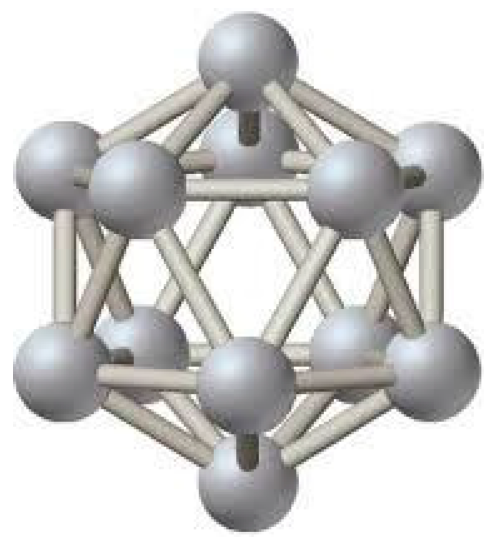
1.1.1. 3-D All-Boron Structures

Boron, the fifth element of the Periodic Table, is located at the intersection of semiconductors and metals. Due to a small covalent radius (only 0.84 Å) and number (only 3) of valence electrons, boron does not form simple three-dimensional structures but crystals with icosahedral clusters with many atoms in the unit cell. At least three all-boron allotropes are known—α- and β-rhombohedral and high-pressure γ-orthorhombic phases—for the experimental phase diagram of boron see Reference [18]. In addition, α- and β-tetragonal and a number of other boron structures, probably stabilized by the presence of impurities/defects, were reported. Theoretical studies of the five boron crystal structures (α, dhcp, sc, fcc, and bcc) were carried out using the LAPW (linearized plane wave) method in Reference [19]. The current state of research on the phase diagram of boron from a theoretical point of view is given in Reference [20]. It should be noted that, in the last decade, several new structures of boron allotropes were discovered and some have been disproved. Currently, even the number of allotropes of boron is uncertain. The reason for this is that there are many such structures, all of them complex, and some of them are minimally different from others. A pseudo-cubic tetragonal boron recently discovered under high-pressure and high-temperature conditions may also be another form of boron allotropes; however, its structure, studied in Reference [21] using a DFT (density functional theory) calculation, is abnormal compared to other allotropes of boron in many ways.
The almost regular icosahedron B12 with B-atoms at the vertices (Figure 1) serves as the main structural motif not only of boron allotropes but also of all known boron-rich compounds. In the boron icosahedron, each atom is surrounded by 5 neighboring atoms and, as usual, with one more atom from the rest of the crystal. For this reason, the average coordination number of a boron-rich lattice ranges from 5 to 5+1=6.
However, an isolated regular boron icosahedron is an electron-deficient structure—the total number of valence electrons of 12 boron atoms is not sufficient to fill all the covalent bonding orbitals corresponding to such a cage-molecule. Thus, if it were a stable structure, then intra-icosahedral bonds would be only partially covalent but also to some extent metallic. As for boron icosahedra constituting real crystals, it was clearly demonstrated, for example, for β-rhombohedral boron [22,23,24,25,26,27], that they are stabilized by the presence of point structural defects—vacancies and interstitials, in other words, both partially filled regular or irregular boron sites—at very high concentrations. For example, in the case of β-rhombohedral boron, the total effect of such a stabilization is to increase the average number of boron atoms inside the unit cell from the ideal value 105 (Figure 2) to 106.7 [28], which leads to the saturation of the electron-deficient orbitals and a 5- or 6-coordination number for the majority of constituent boron atoms.
Thus, all-boron 5- and 6-coordinated regular 3-D lattices cannot exist, but one can naturally imagine 2-D flat or buckled/puckered structures with a triangular arrangement of atoms with and without periodically spaced hexagonal (rarely quadric, pentagonal, or heptagonal) holes. Obviously, most of them are expected to be (semi)metallic. At the moment, a number of different atomic geometries for quasi-planar boron sheets are theoretically proposed [4,5,6,7,29,30,31,32,33,34,35,36,37,38,39,40,41,42,43,44,45,46,47,48,49,50,51].
Using the ab initio evolutionary structure prediction approach, a novel reconstruction of the α-boron (111) surface with the lowest energy was discovered [52]. In this reconstruction, all single interstitial boron atoms bridge neighboring icosahedra by polar covalent bonds, and this satisfies the electron counting rule, leading to the reconstruction-induced semiconductor–metal transition. The new stable boron sheet, called H-borophene, proposed in Reference [53] and constructed by tiling 7-membered rings side by side, should be especially noted.
As for the irregularly distributed holes, they have to be considered as defects. The research [54] is focused on the formation of local vacancy defects and pinholes in a 2-D boron structure—the so-called γ3-type boron monolayer.

1.1.2. Boron Quasi-Planar Clusters

Indirectly, the reality of boron sheets can be proved by the presence of various quasi-planar boron clusters, i.e., finite fragments of sheets, in gaseous state and also boron nanotubes, which are the fragments of boron sheets wrapped into cylinders (see for example, the review from Reference [55] and the references therein). Experimental and theoretical evidences that small boron clusters prefer planar structures were reported in Reference [8].
In addition, recently, a highly stable quasi-planar boron cluster B36 of hexagonal shape with a central hexagonal hole [9], which is viewed as a potential basis for an extended 2-D boron sheet, and boron fullerene B40 [10], which can be imagined as the fragment of a boron sheet wrapped into the sphere, were discovered experimentally. Photoelectron spectroscopy in combination with ab initio calculations have been carried out to probe the structure and chemical bonding of the B27 cluster [56]. A comparison between the experimental spectrum and the theoretical results reveals a 2-D global minimum with a triangular lattice containing a tetragonal defect and two low-lying 2-D isomers, each with a hexagonal vacancy.

1.1.3. Liquid Boron Structure

There are also evidences [57,58,59] that liquid boron does not consist of icosahedra but mainly of quasi-planar clusters. Ab initio MD (molecular-dynamics) simulations of the liquid boron structure yields that at short length scales, B12 icosahedra, a main structural motif of boron crystals and boron-rich solid compounds, are destroyed upon melting. Although atoms form an open packing, they maintain the 6-coordination.
According to measurements of the structure factor and the pair distribution function, the melting process is associated with relatively small changes in both the volume and the short-range order of the system. Results of a comprehensive study of liquid boron with X-ray measurements of the atomic structure and dynamics coupled with ab initio MD simulations also show that there is no evidence of survival of the icosahedral arrangements into the liquid, but many atoms appear to adopt a geometry corresponding to the quasi-planar pyramids.

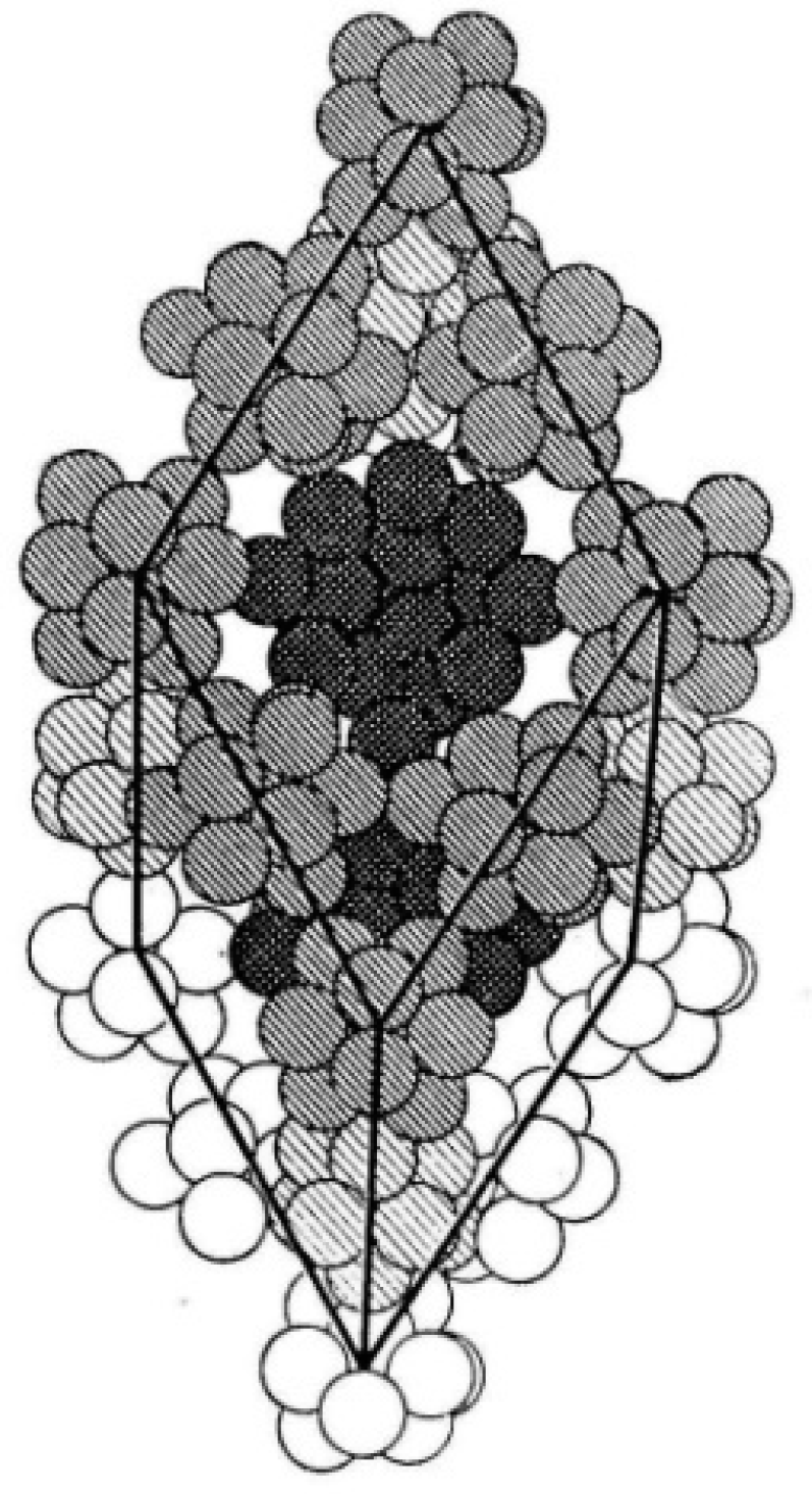
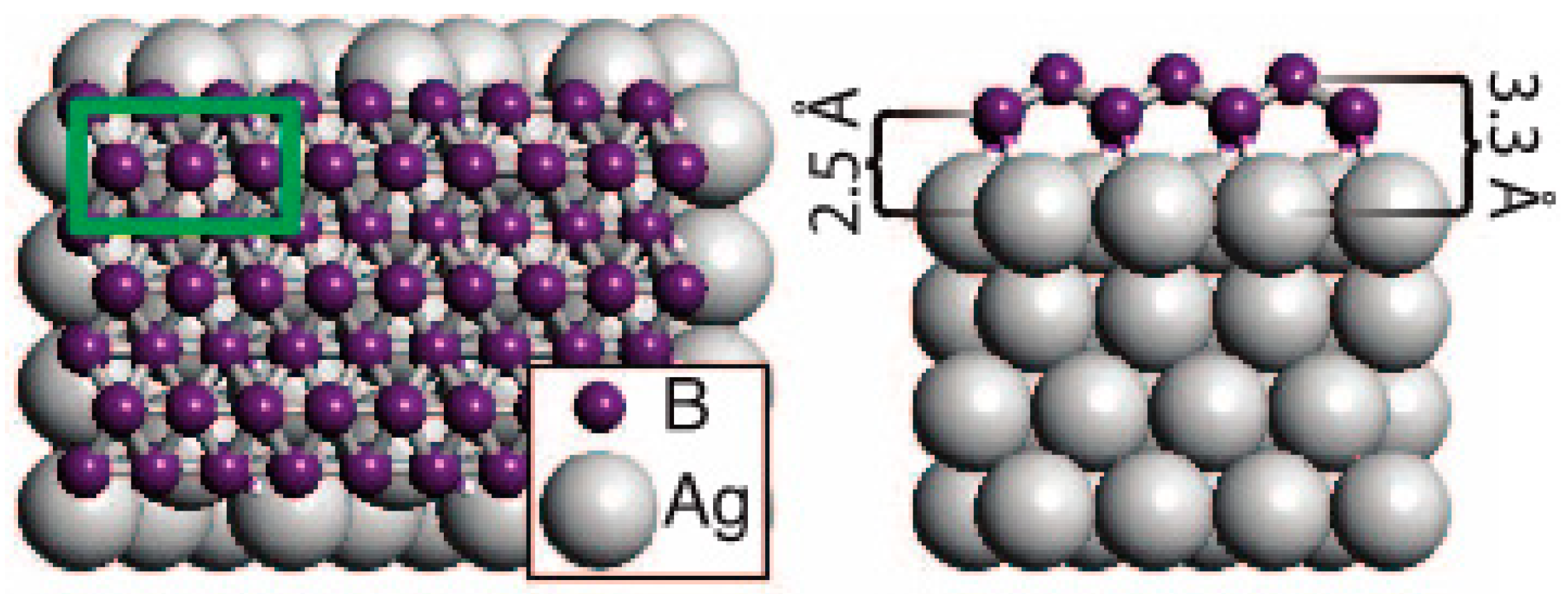
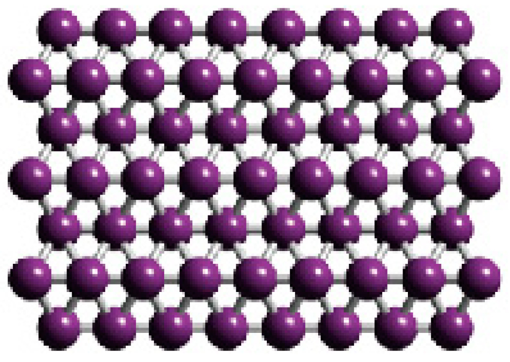
1.1.4. Growing of Boron Sheets

Currently, some of the 2-D materials beyond graphene also are used [60]. But for non-layer structured 3-D materials such as boron, it is a real challenge to fabricate the corresponding 2-D nanosheets due to the absence of the driving force of anisotropic growth. There are rare examples of some 2-D metal nanosheets; see for example, the recent report [61] on single-crystalline Rh nanosheets with a 3–5 atomic layers thickness. Boron sheets are expected to be metallic as well. Thus, this should increase the chances of their actual formation.
In this regard, we have to mention the recent report [62] in which large-scale single-crystalline ultrathin boron nanosheets have been fabricated via the thermal decomposition of diborane.
It is obvious that an infinite boron sheet does not exist in nature and that its finite pieces are not stable compared to bulk and/or nanotubular structures of boron. To grow boron sheets, one needs a substrate which binds boron atoms strongly to avoid bulk phases while, at the same time, provides sufficient mobility of boron atoms on the substrate. Possible candidates for substrates are surfaces of (close-packed transition) metals. The feasibility of different synthetic methods for 2-D boron sheets was assessed [47,63,64,65,66] using ab initio calculations, i.e., “synthesis in theory” approach. A large-scale boron monolayer has been predicted with mixed hexagonal-triangular geometry obtained via either depositing boron atoms directly on the surface or soft landing of small planar B-clusters.
Recently, a series of planar boron allotropes with honeycomb topology has been proposed [67]. Although the free-standing honeycomb B allotropes are higher in energy than α-sheets, these calculations show that a metal substrate can greatly stabilize these new allotropes.
The atomically thin, crystalline 2-D boron sheets, i.e., borophene, were actually synthesized [16] on silver surfaces under ultrahigh-vacuum conditions (Figure 3). An atomic-scale characterization, supported by theoretical calculations, revealed structures reminiscent of fused boron clusters with multiple scales of anisotropic, out-of-plane buckling. Unlike bulk boron allotropes, borophene shows metallic characteristics that are consistent with predictions of a highly anisotropic 2-D metal.
The experimental work in Reference [17] shows that 2-D boron sheets can be grown epitaxially on a Ag(111) substrate. Two types of boron sheets, β12 and χ3, both exhibiting a triangular lattice but with different arrangements of periodic holes, were observed by scanning tunneling microscopy. DFT simulations indicate that both sheets are planar without obvious vertical undulations.
According to the ab initio calculations [68], the periodic nanoscale 1-D undulations can be preferred in borophenes on concertedly reconstructed Ag(111). This “wavy” configuration is more stable than its planar form on flat Ag(111) due to an anisotropic high bending flexibility of borophene. An atomic-scale ultrahigh vacuum scanning tunneling microscopy characterization of a borophene grown on Ag(111) reveals such undulations, which agree with the theory. Although the lattice is coherent within a borophene island, the undulations nucleated from different sides of the island form a distinctive domain boundary when they are laterally misaligned.
Recently, borophene synthesis monitored in situ by low-energy electron microscopy, diffraction, and scanning tunneling microscopy and modeled using ab initio theories has been reported in Reference [69]. By resolving the crystal structure and phase diagram of borophene on Ag(111), the domains are found to remain nanoscale for all growth conditions. However, by growing borophene on Cu(111) surfaces, large single-crystal domains (up to 100 μm) are obtained. The crystal structure is a novel triangular network with a concentration of hexagonal vacancies of η = 1/5. These experimental data together with ab initio calculations indicate a charge-transfer coupling to the substrate without significant covalent bonding.
Boron on a Pb(110) surface was simulated [70] by using ab initio evolutionary methodology and found that 2-D Pmmn structures can be formed because of a good lattice matching. By increasing the thickness of 2-D boron, the three-bonded graphene-like P21/a boron was revealed to possess lower molar energy, indicating the more stable 2-D boron.
The influence of the excess negative charge on the stability of borophenes—2-D boron crystals—was examined in Reference [71] using an analysis of the decomposition of the binding energy of a given boron layer into contributions coming from boron atoms that have different coordination numbers to understand how the local neighborhood of an atom influences the overall stability of the monolayer structure. The decomposition is done for the α-sheet related family of structures. It was found a preference for 2-D boron crystals with very small or very high charges per atom. Structures with intermediate charges are not energetically favorable. It has been also found a clear preference in terms of binding energy for the experimentally observed γ-sheet and δ-sheet structures that is almost independent on the considered excess of negative charge of the structures.
Two-dimensional boron monolayers have been extensively investigated using ab initio calculations [72]. A series of boron bilayer sheets with pillars and hexagonal holes have been constructed. Many of them have a lower formation energy than an α-sheet boron monolayer. However, the distribution and arrangement of hexagonal holes can cause a negligible effect on the stability of these structures.
Recently, an ab initio study [73] of the effect of electron doping on the bonding character and stability of borophene for the neutral system has revealed previously unknown stable 2-D structures: ε-B and ω-B. The chemical bonding characteristic in this and other boron structures is found to be strongly affected by an extra charge. Beyond a critical degree of electron doping, the most stable allotrope changes from ε-B to a buckled honeycomb structure. Additional electron doping, mimicking a transformation of boron to carbon, causes a gradual decrease in the degree of buckling of the honeycomb lattice.

1.2. Applications

In general, the formation of a boron sheet would have wide applications in techniques because the boronizing of metal surfaces is known as an effective method of formation of protective coatings [74]. In particular, quasi-planar bare boron surfaces can serve as lightweight protective armor.
Boron sheets are expected to be very good conductors with potential applications in nanoelectronics, e.g., in high-temperature nanodevices. Boron sheets could have potential as metallic interconnects and wiring in electronic devices and IC (integrated circuits) [41].
A theoretical investigation [32] of both the molecular physisorption and dissociative atomic chemisorption of hydrogen by boron sheets predicts physisorption as the leading mechanism at moderate temperatures and pressures. Further calculations performed on hydrogen-storage properties showed that the decoration of pristine sheets with the right metal elements provide additional absorption sites for hydrogen [47]. Thus, boron sheets can serve for good nanoreservoirs of fuel hydrogen used in green-energy production.
Due to the high neutron-capture cross section of 10B nuclei, solid-state boron allotropies, as well as boron-rich compounds and composites, are good candidates to be used as neutron-protectors. Boron sheets will be especially useful as an absorbing component in composite neutron shields [75]. Materials with the high bulk concentration of B-atoms usually are nonmetals and, therefore, not suitable for electromagnetic shielding purposes. However, frequently, the simultaneous protection against both the neutron irradiation and electromagnetic waves is needed, in particular, because neutron absorption by 10B nuclei is accompanied by a gamma-radiation. For this reason, in the boron-containing nanocomposites designed for neutron-protection, it is necessary to introduce some foreign components with metallic conductivity. Utilizing of the metallic boron sheet as a component may resolve this problem [76].
Recently, the mechanical properties of 2-D boron—borophene—have been studied by ab initio calculations [77]. The borophene with a 1/6 concentration of hollow hexagons is shown to have the Föppl–von Kármán number per unit area over twofold higher than graphene’s value. The record high flexibility combined with excellent elasticity in boron sheets can be utilized for designing advanced composites and flexible devices. The transfer of undulated borophene onto an elastomeric substrate would allow for high levels of stretchability and compressibility with potential applications for emerging stretchable and foldable devices [68].
The boron sheets are quite inert to oxidization and interact only weakly with their substrate. For this reason, they may find applications in electronic devices in the future [17].
In large-scale single-crystalline ultrathin boron nanosheets fabricated [62] via the thermal decomposition of diborane, the strong combination performances of low turn-on field-of-field emissions, favorable electron transport characteristics, high sensitivity, and fast response time to illumination reveal that the nanosheets have high potential as applications in field-emitters, interconnects, IC, and optoelectronic devices.
Some other applications of borophene are described in recent reviews [78,79].

1.3. Available Electron Structure Calculations

Because boron sheets are of great academic and practical interests, their electronic structure is studied intensively. Most of them are found to be metallic.
Let us note that there are some indirect evidences for metallic conduction in boron sheets. The absence of icosahedra in liquid boron affects its properties including electrical conductivity [57,59], and it behaves like a metal.
The very stable quasi-planar clusters of boron Bn for n up to 46, considered to be fragments of bare boron quasi-planar surfaces, have to possess a singly occupied bonding orbital [29]. Assuming that conduction band of the infinite surface is generated from the HOMO (highest-occupied-molecular-orbital) of a finite fragment, it means the partial filling of the conduction band, i.e., the metallic mechanism of conductance.
Diamond-like, metallic boron crystal structures were predicted in Reference [80] employing so-called decoration schemes of calculations, in which the normal and hexagonal diamond-like frameworks are decorated with extra atoms across the basal plane. They should have an overly high DoS near the Fermi level. This result may provide a plausible explanation for not only the anomalous superconductivity of boron under high pressure but also the nonmetal–metal transition in boron structures.
In Reference [45], it was presented the results of a theoretical study of the phase diagram of elemental boron showing that, at high pressures, boron crystallizes in quasi-layered bulk phases characterized by in-plane multicenter bonds and out-of-plane bonds. All these structures are metallic.
Usually, direct ab initio calculations performed for boron sheets of different structures reveal the pronounced metallic-like total DoSs [4,5,7,30,31,35,38,40,41,44,46,64], and therefore, boron sheets show a strongly conducting character.
Band structures of a series of planar boron allotropes with honeycomb topologies recently proposed in Reference [67], exhibit Dirac cones at the K-point, the same as in graphene. In particular, the Dirac point of honeycomb boron sheet locates precisely on the Fermi level, rendering it as a topologically equivalent material to graphene. Its Fermi velocity is of 6·105 m/s, close to that of graphene. However, in H-borophene [53] constructed by tiling 7-membered rings side by side, a Dirac point appeared at about 0.33 eV below the Fermi level.
According to some theoretical results [36,37,47,48], boron sheets can be not only metal but in some cases also an almost zero band-gap semiconductor depending on its atomistic configuration. Probably, the semiconducting character is related to the nonzero thickness of buckled/puckered 2-D boron sheets or double-layered structures.
Some of borophenes can be magnetic. Based on a tight-binding model of 8-Pmmn borophene developed in Reference [81], it is confirmed that the crystal hosts massless Dirac fermions and the Dirac points are protected by symmetry. Strain is introduced into the model, and it is shown to induce a pseudomagnetic field vector potential and a scalar potential. The 2-D antiferromagnetic boron, designated as M-boron, has been predicted [82] using an ab initio evolutionary methodology. M-boron is entirely composed of B20 clusters in a hexagonal arrangement. Most strikingly, the highest valence band of M-boron is isolated, strongly localized, and quite flat, which induces spin polarization on either cap of the B20 cluster. This flat band originates from the unpaired electrons of the capping atoms and is responsible for magnetism. M-boron is thermodynamically metastable.
Boron sheets grown on metal surfaces are predicted [63] to be strongly doped with electrons from the substrate, showing that a boron sheet is an electron-deficient material. As mentioned, by simulating [70] boron on Pb(110) surface using ab initio evolutionary methodology, it was found that the 2-D Dirac Pmmn boron can be formed. Unexpectedly, by increasing the thickness of 2-D boron, the three-bonded graphene-like structure P21/a was revealed to possess double anisotropic Dirac cones. It is the most stable 2-D boron with particular Dirac cones. The puckered structure of P21/a boron results in the peculiar Dirac cones.
This present work aims to provide more detailed calculations on the electronic structure of boron sheet including not only DoS but also band structure, electron effective mass, Fermi curve, etc.

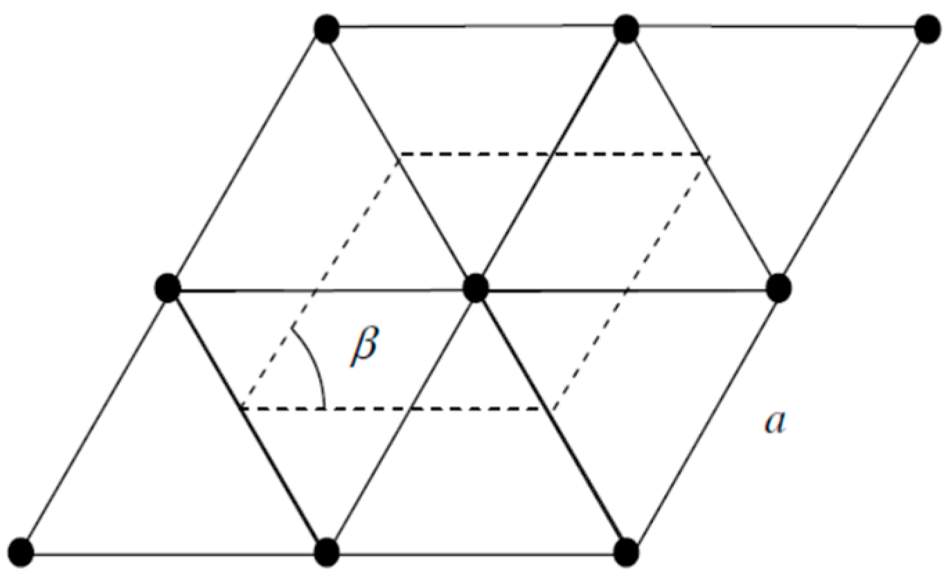
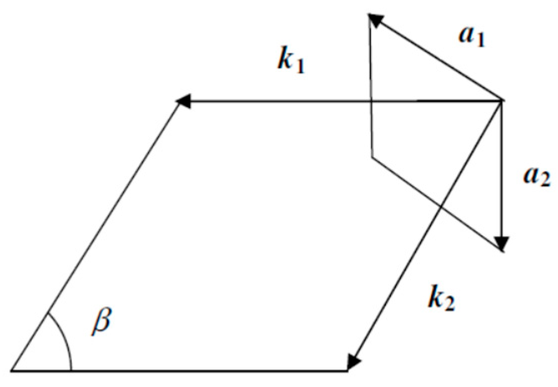
2. Theoretical Approach

We use an original theoretical method of the quasi-classical type [83] based on the proof that the electronic system of any substance is a quasi-classical system; that is, its exact and quasi-classical energy spectra are close to each other.
This approach successfully was applied to all-boron structures to determine their structural parameters, binding energy, vibrational frequencies, and isotopic effects as well; see for example, References [84,85,86,87,88].
As for the determination of the materials’ electron structure, the quasi-classical method is reduced to the LCAO (linear combination of atomic orbitals) method with a basis set of quasi-classical atomic orbitals. Within the initial quasi-classical approximation, the solution of the corresponding mathematical problem consists of two main stages:
  • The construction of matrix elements for secular equation, which, within the initial quasi-classical approximation, reduces to a geometric task of determining the volume of the intersection of three spheres [89], and
  • The solving of the secular equation, which determines the crystalline electronic energy spectrum [90].
This method has been successfully applied to electronic structure calculations performed for various modifications of boron nitride, BN, one of the most important boron compounds [91,92,93,94], as well as metal-doped β-rhombohedral boron [95].
The maximal relative error of a quasi-classical calculation itself, i.e., without errors arisen from input data, is estimated as approx. 4%.
As for the input data, the quasi-classical method of band structure calculations requires them to be in the form of quasi-classical parameters of constituent atoms: the inner and outer radii of the classical turning points for electron states in atoms, the radii of layers of the quasi-classical averaging of potential in atoms, and the averaged values of the potential within corresponding radial layers of atoms. These quantities for an isolated boron atom (as well as for other atoms) in the ground state were pre-calculated in Reference [96] on the basis of ab initio theoretical, namely Hartree–Fock (HF), values of electron levels [97]. Thus, in our case, the accuracy of the quasi-classical parameters is determined by that of the HF approach.
As is known, the electronic structure of any atomic system is influenced by its geometric structure and vice versa. Often, one starts with the question of how to find the most stable idealized atomic configuration. Despite this, here, we will directly begin with the electron band structure of a flat triangular boron sheet, neglecting the buckling/puckering effects and hexagonal holes (see references above), assuming that in real sheets (e.g., grown on metal surfaces), their buckled/puckered or vacant parts would not be arranged in a periodic manner, and thus, they should be regarded as perturbations which can be taken into account within a higher-order perturbation theory.
Multi-layered (buckled) boron sheets can be imagined by substituting metal Me atoms again with boron B atoms in the layered structure of a metal boride MeB2. Analyses of the isolated layer instead of multilayered structure also seems to be quite sufficient for the initial approximation because, in such structures, only intra-layer conductivity is metallic, while interlayer conductivity is nonmetallic due to larger interlayer bond lengths if compared with those in layers.
The 2-D unit cell of the perfectly flat boron sheet without hexagonal holes (Figure 4) is a rhomb with an acute angle of β = π / 3 , i.e., with a single lattice constant a (Figure 5). Let a 1 and a 2 be lattice vectors, a 1 = a 2 = a . Then, the radius-vectors of the lattice sites are n 1 a 1 + n 2 a 2 with n 1 , n 2 = , 3 , 2 , 1 , 0 , + 1 , + 2 , + 3 , . Vectors k 1 and k 2 of a reciprocal lattice (Figure 6) have to be determined from the relations k 1 a 2 , k 2 a 1 , and k 1 = k 2 = 4 π / 3 a . There is a number of different values for the lattice constant of a boron sheet suggested theoretically. For the self-consistency of calculations, we use a = 3.37 a.u. of length, i.e., 1.78 Å, which corresponds to the B–B pair interatomic potential in the same quasi-classical approximation [91].
Into the basis set of a simple LCAO formalism, it has been included core (1s), fully (2s), and partially filled (2p) valence and empty excited (2p) atomic orbitals.
Experimentally, there are 10 detected different existing states in the boron atom. To minimize the calculation errors related to the approximation of the crystalline potential by the superposition of atomic potentials, we choose orbitals with the same symmetry as the partially filled valence orbital, i.e., 2p, with the closest energy level and, consequently, with the closest classical turning point radii of electrons.
Taking into account the degeneracy of atomic energy levels by magnetic and spin quantum numbers of 2, 2, 6, and 6, respectively, we can state that this set of 4 orientation-averaged orbitals replaces 16 angularly dependent atomic orbitals.
The secular equation takes the form
det ( H ( α 1 , α 2 ) E ( α 1 , α 2 ) S ( α 1 , α 2 ) ) = 0
where S ( α 1 , α 2 ) and H ( α 1 , α 2 ) are 16 × 16 matrices of overlapping integrals and single-electron Hamiltonian, respectively, reducible to 4 × 4 matrices. E ( α 1 , α 2 ) is a required electron energy band. About the parameters α 1 and α 2 , see below.
This equation has 4 different real and negative roots E m ( α 1 , α 2 ) , m = 1 , 2 , 3 , 4 . It can be demonstrated that they exhibit all the different solutions of the corresponding secular equation with 16 × 16 matrices. Within the initial quasi-classical approximation, these matrix elements can be found from the relations shown in the Appendix.
Formally, these expressions contain infinite series. However, within the initial quasi-classical approximation, due to the finiteness of quasi-classical atomic radii, only a finite number of summands differs from zero. Thus, the series are terminated unambiguously.
The input data in a.u. in the form of quasi-classical parameters of boron atoms are shown in Table 1 and Table 2. As it was mentioned above, the parameters of electron states fully or partially filled with electrons in the ground state were calculated on the basis of the theoretical, namely HF, values of electron levels, while for the excited state, we use the experimental value [98], which, however, is modulated by the multiplier of order of 1, 0.984151, leading to the coincidence between experimental and HF-theoretical first ionization potentials for an isolated boron atom: 0.304945 and 0.309856 a.u., respectively. Note that for the ground state, the 1s22s22p configuration is considered, not the 1s22s2p2 configuration, from which the ground state and first excited states of some boron-like ions arise [99].
All the matrix elements and electron energies are calculated in points α 1 k 1 + α 2 k 2 of the reciprocal space with parameters 1 / 2 α 1 , α 2 + 1 / 2 , i.e., within a rhombic unit cell of the reciprocal lattice (Figure 7). The first Brillouin zone for a boron flat sheet has a hexagonal shape. Of course, the areas of hexagonal and rhombic unit cells are equal (Figure 8).
The unit cell is covered evenly by 1,002,001 points, at which the energy is found as a solution to the generalized eigenvalue problem.
The calculation has been performed in atomic units, a.u. Then, the results have been converted according to the relations: 1 a.u. of energy = 27.212 eV and 1 a.u. of length = 0.52918 Å.
Based on the resulting data set, we have constructed the electron band surfaces, the distribution of DoS in the bands, and the Fermi curve, emphasizing that, instead of the Fermi surface, the characteristics of 3-D crystals, 2-D crystals are characterized by Fermi curves.

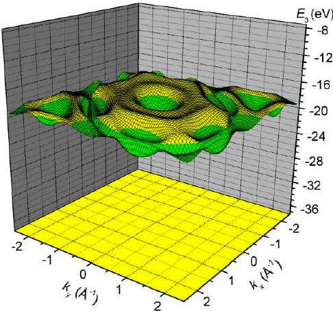
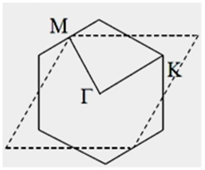
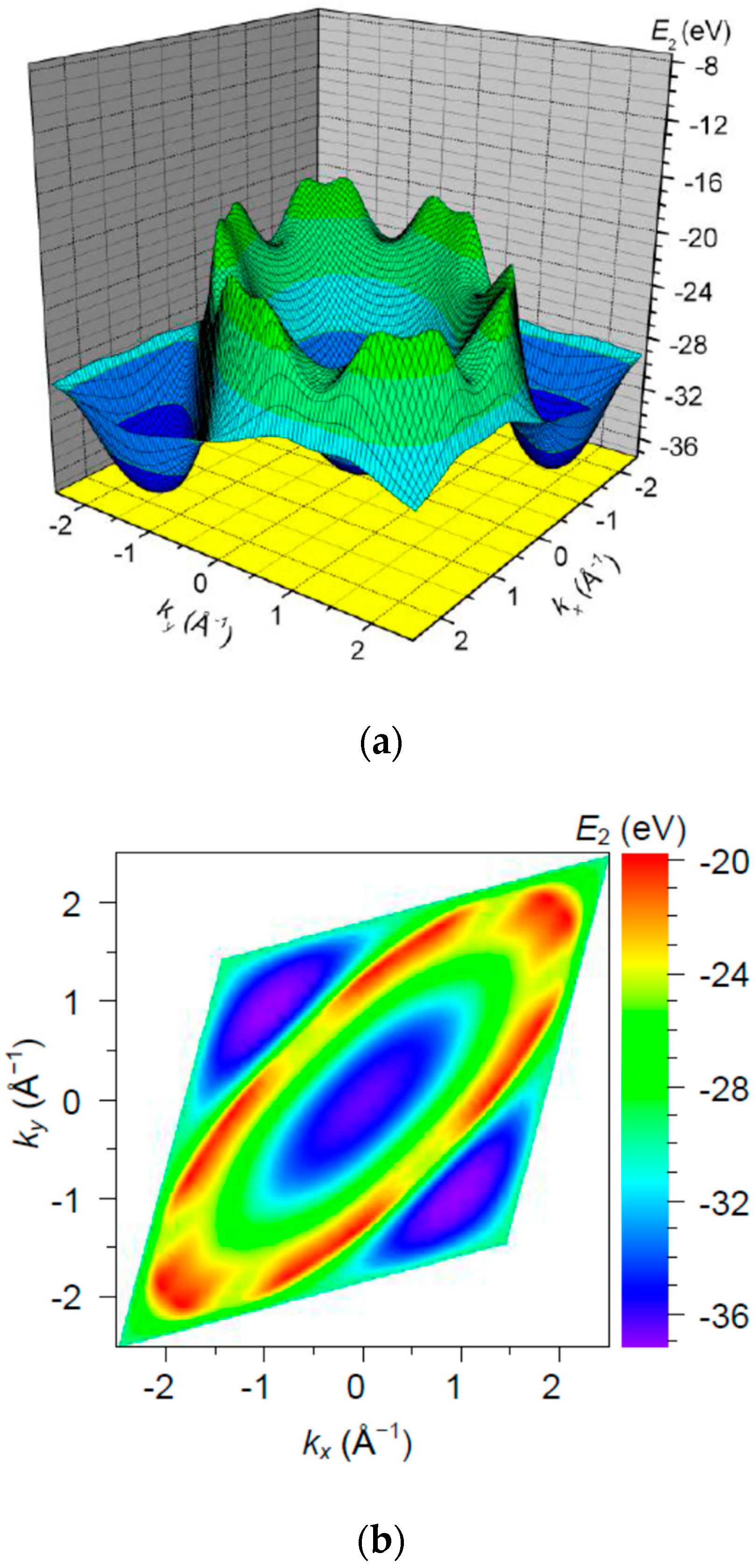
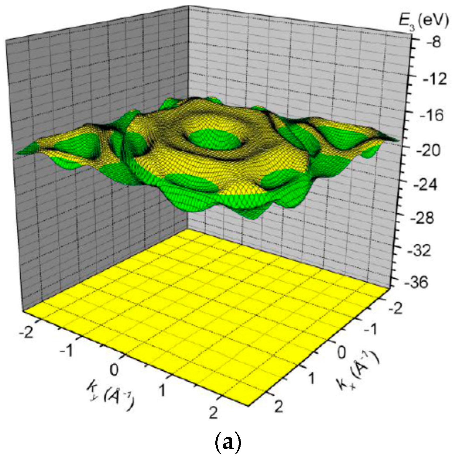
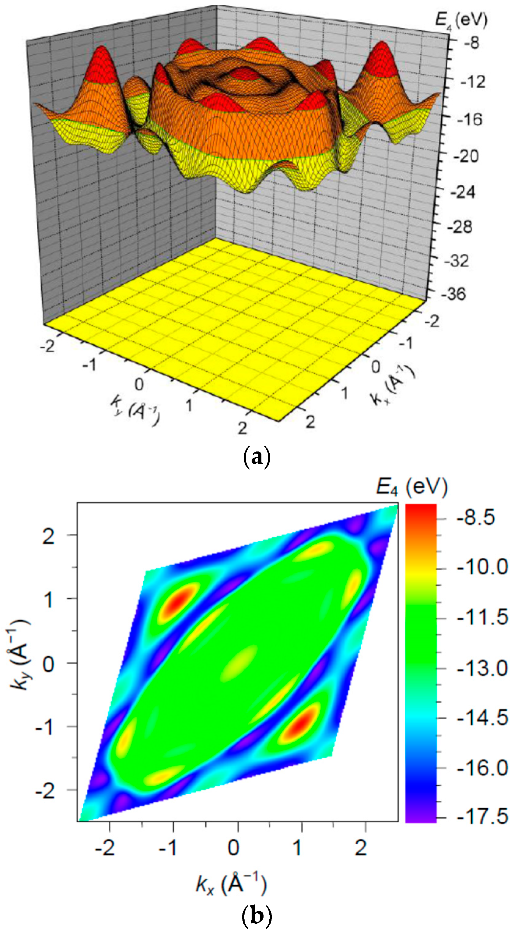
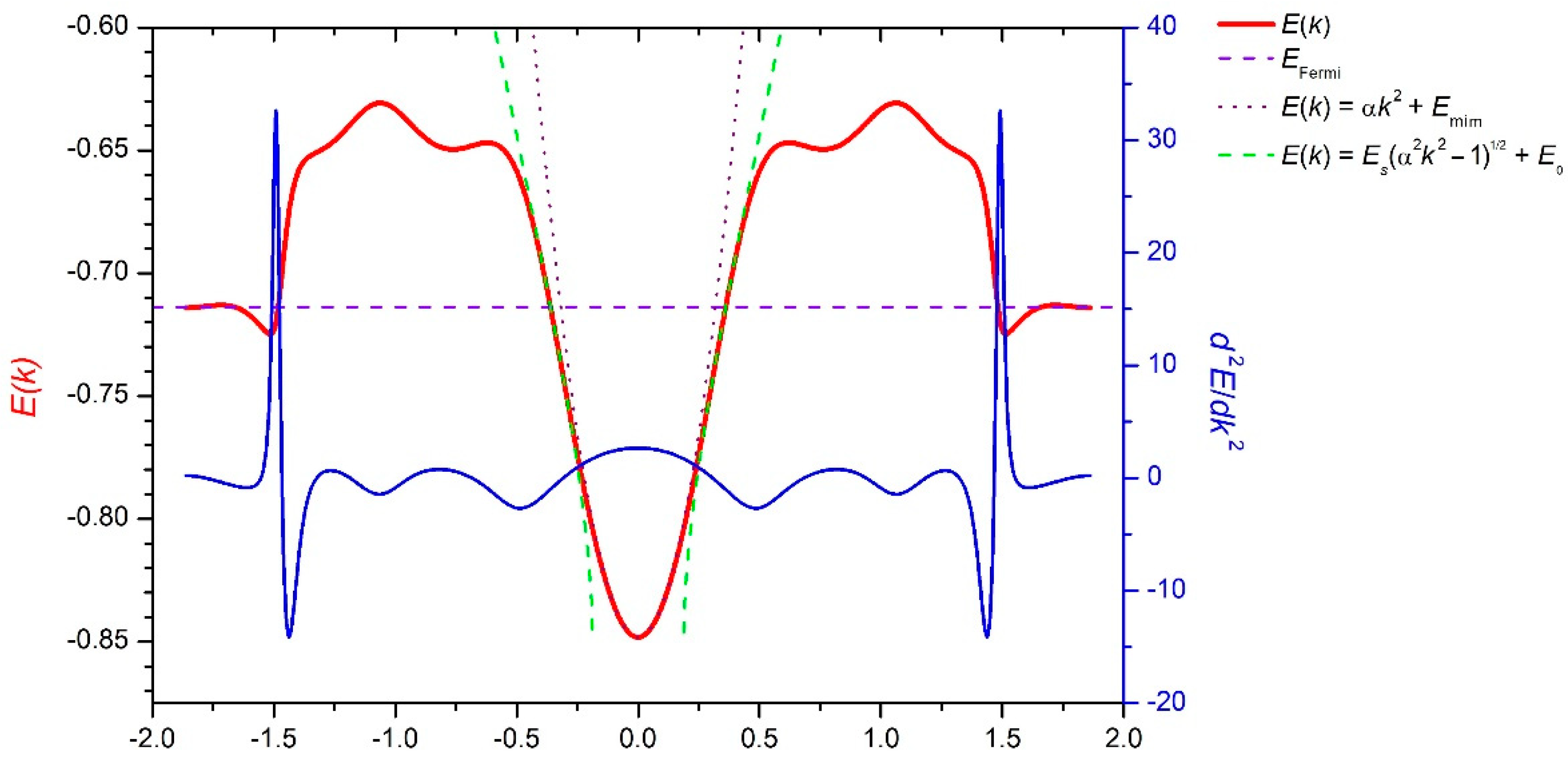
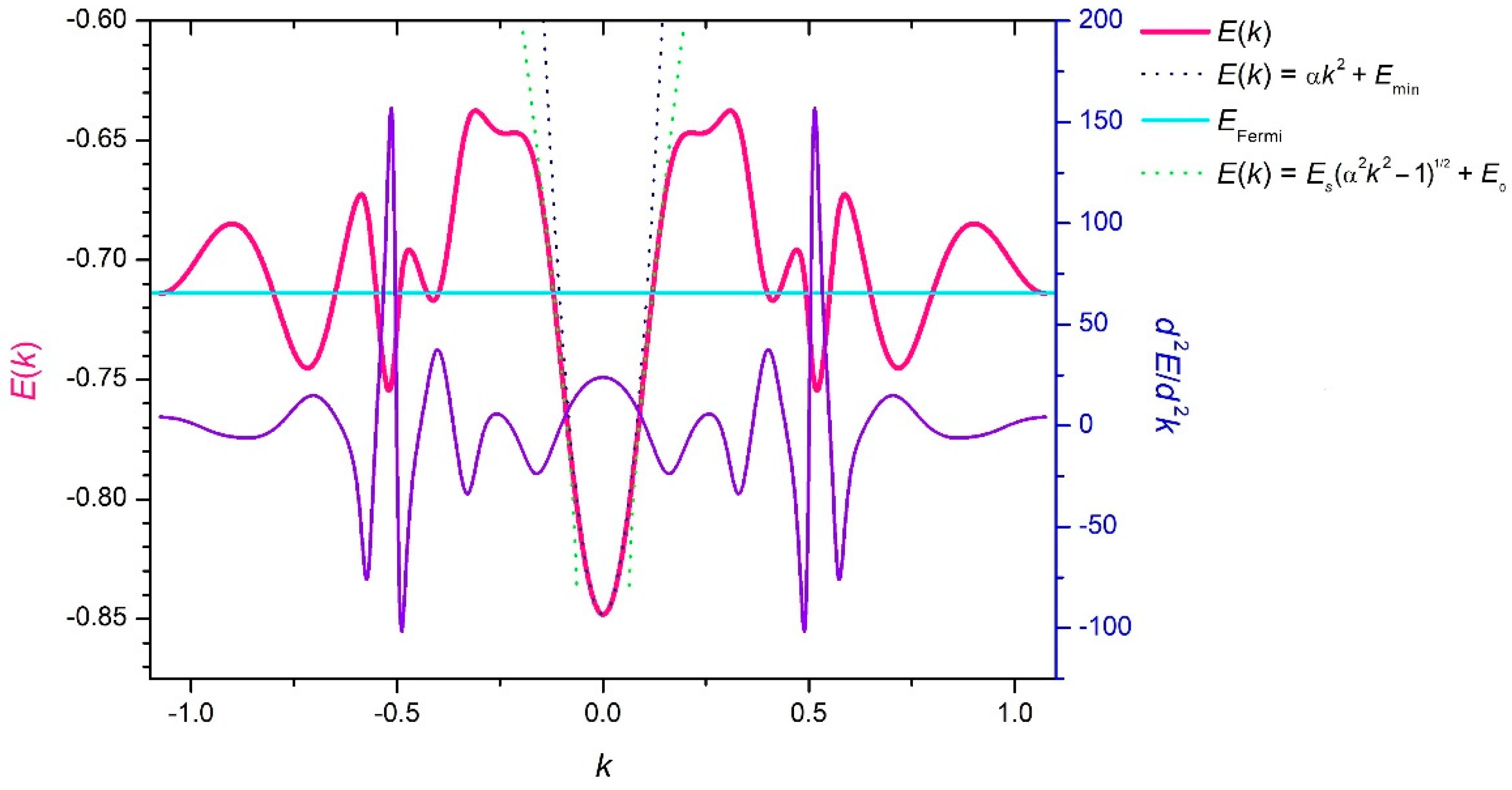
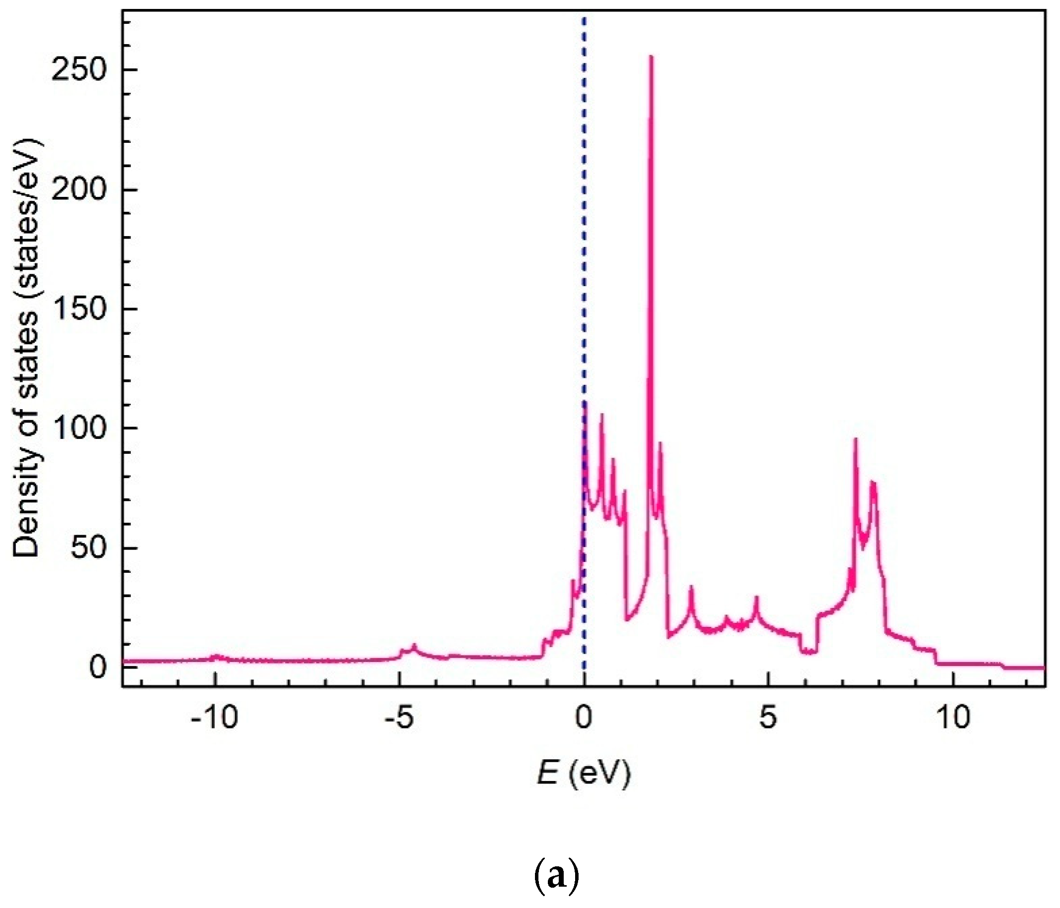
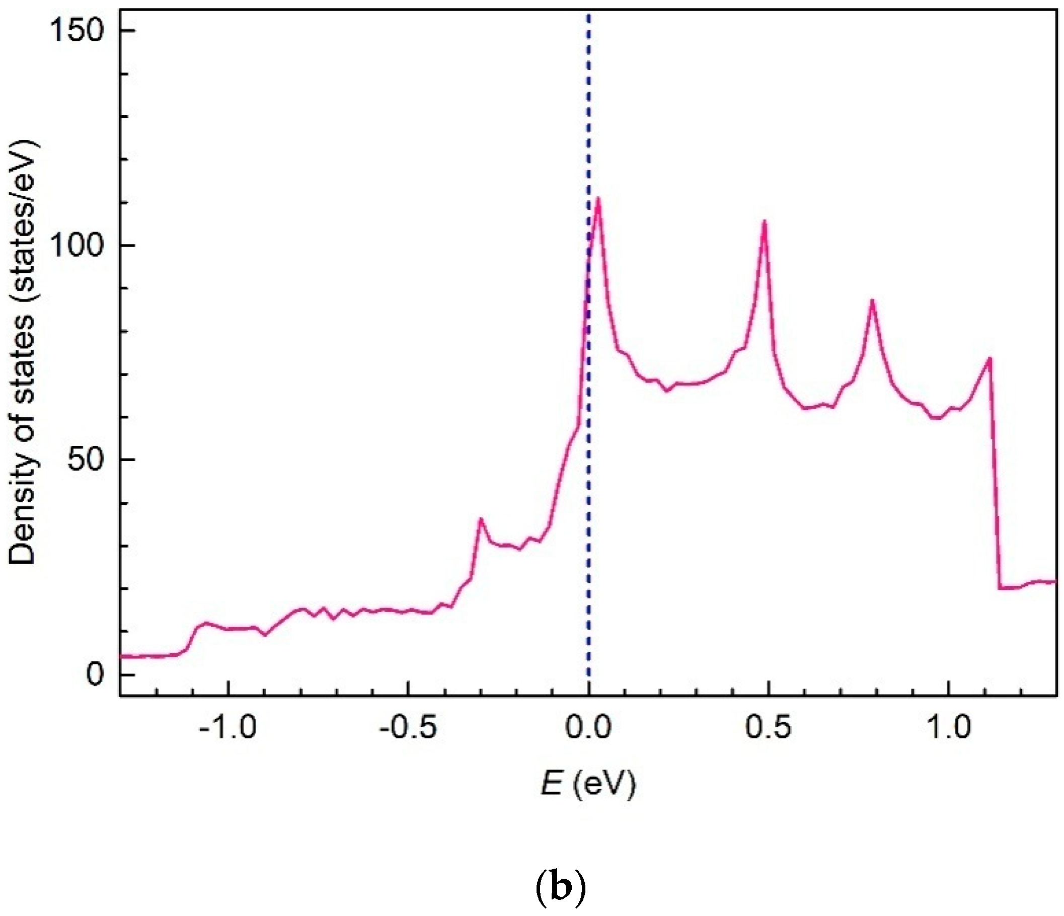
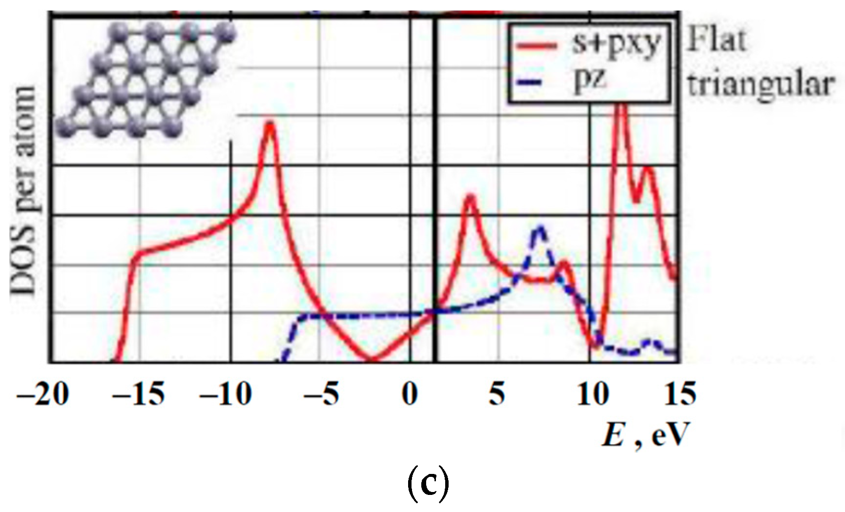
3. Results and Discussion

In the quasi-classically calculated electronic structure of the flat boron sheet, we resolve four bands of energy. We have to emphasize that for simplicity, the band surfaces below are shown over a rhombic (not hexagonal) domain.
The lowest energy band E 1 surface is found to be almost a plane placed at the level of E 1 min = E 1 max = 276.21   eV . Thus, the chemical shift against the core 1s atomic level E 1 s = 209.41 eV equals to δ E 1 = E 1 s E 1 = 66.80   eV . Dispute the shift of the B 1s atomic level, it retains an order of magnitude after transforming in an electronic band of the boron flat sheet. The lowest-lying band E 1 is fully filled with electrons.
The band E 2 is the highest fully filled band (Figure 9) with bottom at E 2 min = 37.21   eV and top at E 2 max = 19.85   eV , i.e., with a width of Δ E 2 = E 2 max E 2 min = 17.36   eV . Note that, this range of energies is comparable in order of magnitude with a valence 2s atomic level of E 2 s = 13.46   eV .
The band E 3 (Figure 10) is partially filled, i.e., partially empty, with a bottom at E 3 min = 23.08   eV and top at E 3 max = 17.16   eV , i.e., with a width of Δ E 3 = E 3 max E 3 min = 5.92   eV . Note that this range of energies is comparable in order of magnitude with a valence 2p atomic level E 2 p = 8.43   eV .
The band E 4 (Figure 11) is empty, with a bottom at E 4 min = 17.65   eV and top at E 4 max = 8.08   eV , i.e., with a width of Δ E 4 = E 4 max E 4 min = 9.57   eV . Note that this range of energies is comparable in order of magnitude with the modulated value of the excited 2p level E 2 p = 5.84   eV .
Between bands E 1 and E 2 , there is a very wide energy gap of Δ E 12 = E 2 min E 1 max = 239.00   eV , while pairs of bands E 2 and E 3 , and E 3 and E 4 overlap each with other, i.e. there are obtained pseudo-gaps of Δ E 23 = E 3 min E 2 max = 3.23   eV and Δ E 34 = E 4 min E 3 max = 0.49   eV .
The Fermi level is found at E Fermi = 19.42   eV , within the part of the band E 3 without overlapping with other bands. This result confirms the metallicity of the boron sheet.
Thus, all the electron energies are found to be negative. It means that all electrons, including conduction electrons at the Fermi level, are bounded inside the 2-D crystal. This result once more evidences the correctness of the calculations performed in this work. The total width of valence and conduction bands equal to Δ E V = E Fermi E 2 min = 17.79   eV and Δ E C = E 4 max E Fermi = 11.34   eV , respectively. The upper valence band width is Δ E VU = E Fermi E 2 max = 0.43   eV . As expected, it is negligible if compared with that of a conduction band.
To compare easily our results with the literature data, in addition to the presentation of the band structure using the contour plots of the whole Brillouin zone in Figure 12 and Figure 13, we plot the band energies (as well as their second derivatives and corresponding parabolic approximations) along the main lines of symmetry.
Our quasi-classical calculation of the crystalline band structure, like any other approach also utilizing HF parameters of constituting atoms, cannot determine the absolute values of energy parameters with a high accuracy. By this reason, the above mentioned value E Fermi cannot be used directly to determine the electron work function of the boron sheet. This goal can be achieved only after corrections are made to include the electron-correlation and to exclude the electron-self-interacting effects, which have to allow an accurate determination of the position for the vacuum level of energy E = 0 . However, the shifting of the reference point at the energy axis does not affect the energy differences, which are credible as are determined with quite an acceptable accuracy. They are collected in Table 3.
The Fermi curve of a boron flat sheet is found to be consisting of parts of a number of closed curves including concentric ones, the centre of which can be approximated by ellipse with long and short axes along the Γ–K and Γ–M directions, respectively (Figure 14).
As it is known, for semiconductors, the effective mass conception referring to band zone curvatures is used to approximate the wave-vector dependence of electron energies near the band gap. As for metals, the Fermi surface curvature can be used to estimate the effective mass of conduction electrons and hence their mobility.
The ellipse representing a branch of intersection between the E 3 -band surface with the E Fermi -plane can be described by the equation
2 k Γ K 2 2 m Γ K + 2 k Γ M 2 2 m Γ M = F
where k Γ K and k Γ M are wave-number components along perpendicular axes Γ–K and Γ–M and F = E Fermi E 3 min = 3.66   eV is the Fermi energy. The effective masses m Γ K and m Γ M can be estimated from this equation if it is rewritten in the form of a normalized ellipse equation
k Γ K 2 k Γ K    0 2 + k Γ M 2 k Γ M    0 2 = 1
where k Γ K     0 and k Γ M     0 are half-axes in the directions Γ–K and Γ–M, respectively:
k Γ K     0 = 2 m Γ K F 0.679 / Å
and
k Γ M     0 = 2 m Γ M F 0.224 / Å .
Then, one can calculate the effective mass of the conduction electrons m σ , i.e., electrons placed at the Fermi level, from the relation
2 m σ = 1 m Γ K + 1 m Γ M
The effective electron mass at the Fermi level reveals a significant anisotropy. For the central ellipse, the effective masses are m Γ K / m 0 0.480 and m Γ M / m 0 0.052 , with m σ / m 0 0.094 , where m 0 is the free electron mass.
The Fermi curve of a boron flat sheet is found to consist of 6 parts of 3 ellipses representing the quadric energy-dispersion of the conduction electrons; see Figure 15.
DoS within the bands E 2 , E 3 , and E 4 against electron energy renormalized to the Fermi level E E E Fermi are presented in Figure 16 in two different scales for the convenient consideration. As for the band E 1 , DoS within this band is proportional to the Dirac function, ~ δ ( E + 256.42   [ eV ] ) , with the accordingly renormalized argument 276.21   eV 276.21   eV ( 19.42   eV ) = 256.79   eV .
The overall shapes of DoSs obtained by us and previously by others, especially, in References [31,33,47] are rather similar but with some differences. It is understandable as these structures are buckled/puckered or flat variants of the same triangular lattice with or without hexagonal holes (Figure 17). The discrepancies may be attributed with the perturbations related to the mentioned structural changes and differences between the computing methods utilized, as well as the difference between projected onto in-plane or out-of-plane orbitals’ densities-of-states (PDoSs) from the total DoS of the sheet.
The Fermi curve of the monolayer flat boron sheet approximated by parts of concentric closed ellipse-like curves could be considered as a certain kind of topological analog of the Fermi surface (Figure 18) in the form of a half-torus and distorted cylinder of magnesium diboride MgB2 [100], which is believed to be a structural analog of the hypothetical multilayered boron sheet, where metal Me atoms in a metal diboride MeB2 structure are replaced by B-atoms themselves.
The low effective mass of conduction electrons at the Fermi level indicates a high mobility of electrons and, hence, a high conductivity of the flat boron sheet.

4. Conclusions

In summary, we can conclude that the electronic band structure of a boron flat triangular sheet has been calculated within a quasi-classical approach for the quasi-classical structural parameter (B–B bond length) of a = 1.78 Å. It is shown to have metallic properties like most of other modifications of boron sheets.
There are resolved four electronic bands: E 1 , E 2 , E 3 , and E 4 . The bands’ widths are Δ E 1 = 0.00 , Δ E 2 = 17.36 , Δ E 3 = 5.92 , and Δ E 4 = 9.57   eV , respectively. The (pseudo)gaps between the bands are Δ E 12 = 239.00 , Δ E 23 = 3.23 , and Δ E 34 = 0.49   eV . The Fermi level E Fermi is located within the filled band E 3 , confirming the metallicity of the boron flat sheet.
The Fermi curve of a boron flat sheet consists of parts of 3 ellipses with semimajor and semiminor axes along the Γ–K and Γ–M directions, respectively. The effective electron mass at the Fermi level reveals a distinct anisotropy: m Γ K / m 0 0.480 and m Γ M / m 0 0.052 , with m σ / m 0 0.094 for conduction mass. The low effective mass of conduction electrons indicates a high mobility of electrons and, hence, a high conductivity of flat boron sheets.
The shapes of density-of-states obtained here for flat holeless boron sheets and previously calculated ones are rather similar, which is understandable as these structures are buckled/puckered or flat but with hexagonal holes, variants of the same triangular lattice. The remaining discrepancies may be attributed to the perturbations associated with the mentioned structural changes and differences in the used models.

Author Contributions

Conceptualization, L.C. and R.B.; methodology, L.C.; software, I.M.; validation, L.C., I.M., and R.B.; formal analysis, I.M.; investigation, L.C., I.M., and R.B.; resources, L.C. and R.B.; data curation, I.M.; writing—original draft preparation, L.C.; writing—review and editing, I.M.; visualization, L.C. and I.M.; project administration, L.C.

Funding

This research was funded by Shota Rustaveli National Science Foundation of Georgia (SRNSFG), Grant AR–18–1045: “Obtaining of boron carbide-based nanostructured heterophase ceramic materials and products with improved performance characteristics”.

Conflicts of Interest

The authors declare no conflict of interest. The funder had no role in the design of the study; in the collection, analyses, or interpretation of data; in the writing of the manuscript; or in the decision to publish the results.

Appendix A

Within the initial quasi-classical approximation, the matrix elements of overlapping integrals S ( α 1 , α 2 ) and single-electron Hamiltonian H ( α 1 , α 2 ) can be respectively found from following explicit relations:
S j l ( α 1 , α 2 ) = 3 4 π n 1 = n 1 = + n 2 = n 2 = + V j l ( n 1 , n 2 ) ( r j 3 r j 3 ) ( r l 3 r l 3 ) cos 2 π ( n 1 α 1 + n 2 α 2 ) V j l ( n 1 , n 2 ) = = V ( r j , r l , a n 1 2 + n 1 n 2 + n 2 2 ) + + V ( r j , r l , a n 1 2 + n 1 n 2 + n 2 2 ) V ( r j , r l , a n 1 2 + n 1 n 2 + n 2 2 ) V ( r j , r l , a n 1 2 + n 1 n 2 + n 2 2 )
and
H j l ( α 1 , α 2 ) = 3 4 π n 1 = n 1 = + n 2 = n 2 = + ν 1 = ν 1 = + ν 2 = ν 2 = + λ = 1 λ = 5 φ λ V j l λ ( n 1 , n 2 , ν 1 , ν 2 ) ( r j 3 r j 3 ) ( r l 3 r l 3 ) cos 2 π ( n 1 α 1 + n 2 α 2 ) V j l λ ( n 1 , n 2 , ν 1 , ν 2 ) = = V ( r j , r l , r λ , a n 1 2 + n 1 n 2 + n 2 2 , a ν 1 2 + ν 1 ν 2 + ν 2 2 , a ( n 1 ν 1 ) 2 + ( n 1 ν 1 ) ( n 2 ν 2 ) + ( n 2 ν 2 ) 2 ) + + V ( r j , r l , r λ 1 , a n 1 2 + n 1 n 2 + n 2 2 , a ν 1 2 + ν 1 ν 2 + ν 2 2 , a ( n 1 ν 1 ) 2 + ( n 1 ν 1 ) ( n 2 ν 2 ) + ( n 2 ν 2 ) 2 ) + + V ( r j , r l , r λ 1 , a n 1 2 + n 1 n 2 + n 2 2 , a ν 1 2 + ν 1 ν 2 + ν 2 2 , a ( n 1 ν 1 ) 2 + ( n 1 ν 1 ) ( n 2 ν 2 ) + ( n 2 ν 2 ) 2 ) + + V ( r j , r l , r λ , a n 1 2 + n 1 n 2 + n 2 2 , a ν 1 2 + ν 1 ν 2 + ν 2 2 , a ( n 1 ν 1 ) 2 + ( n 1 ν 1 ) ( n 2 ν 2 ) + ( n 2 ν 2 ) 2 ) V ( r j , r l , r λ , a n 1 2 + n 1 n 2 + n 2 2 , a ν 1 2 + ν 1 ν 2 + ν 2 2 , a ( n 1 ν 1 ) 2 + ( n 1 ν 1 ) ( n 2 ν 2 ) + ( n 2 ν 2 ) 2 ) V ( r j , r l , r λ , a n 1 2 + n 1 n 2 + n 2 2 , a ν 1 2 + ν 1 ν 2 + ν 2 2 , a ( n 1 ν 1 ) 2 + ( n 1 ν 1 ) ( n 2 ν 2 ) + ( n 2 ν 2 ) 2 ) V ( r j , r l , r λ 1 , a n 1 2 + n 1 n 2 + n 2 2 , a ν 1 2 + ν 1 ν 2 + ν 2 2 , a ( n 1 ν 1 ) 2 + ( n 1 ν 1 ) ( n 2 ν 2 ) + ( n 2 ν 2 ) 2 ) V ( r j , r l , r λ 1 , a n 1 2 + n 1 n 2 + n 2 2 , a ν 1 2 + ν 1 ν 2 + ν 2 2 , a ( n 1 ν 1 ) 2 + ( n 1 ν 1 ) ( n 2 ν 2 ) + ( n 2 ν 2 ) 2 ) ,
where V ( R 1 , R 2 , D 12 ) and V ( R 1 , R 2 , R 3 , D 12 , D 13 , D 23 ) are intersection volumes of two and three spheres, respectively, with radii R 1 , R 2 , and R 3 and intercentral distances D 12 , D 13 , and D 23 .

References

  1. Becker, R.; Chkhartishvili, L.; Martin, P. Boron, the new graphene? Vac. Technol. Coat. 2015, 16, 38–44. [Google Scholar]
  2. Boustani, I. Systematic ab initio investigation of bare boron clusters: Determination of the geometry and electronic structures of Bn (n=12–14). Phys. Rev. B 1997, 55, 16426–16438. [Google Scholar] [CrossRef]
  3. Boustani, I.; Rubio, A.; Alonso, J.A. Ab initio study of B32 clusters: Competition between spherical, quasiplanar and tubular isomers. Chem. Phys. Lett. 1999, 311, 21–28. [Google Scholar] [CrossRef]
  4. Boustani, I.; Quandt, A.; Hernandez, E.; Rubio, A. New boron based nanostructured materials. J. Chem. Phys. 1999, 110, 3176–3185. [Google Scholar] [CrossRef]
  5. Boustani, I.; Quandt, A.; Rubio, A. Boron quasicrystals and boron nanotubes: Ab initio study of various B96 isomers. J. Solid State Chem. 2000, 154, 269–274. [Google Scholar] [CrossRef]
  6. Mukhopadhyay, S.; He, H.; Pandey, R.; Yap, Y.K.; Boustani, I. Novel spherical boron clusters and structural transition from 2D quasi-planar structures to 3D double-rings. J. Phys. Conf. Ser. 2009, 176, 012028. [Google Scholar] [CrossRef] [Green Version]
  7. Ozdogan, C.; Mukhopadhyay, S.; Hayami, W.; Guvenc, Z.B.; Pandey, R.; Boustani, I. The unusually stable B100 fullerene, structural transitions in boron nanostructures, and a comparative study of α- and γ-boron and sheets. J. Phys. Chem. C 2010, 114, 4362–4375. [Google Scholar] [CrossRef]
  8. Zhai, H.-J.; Kiran, B.; Li, J.; Wang, L.-S. Hydrocarbon analogues of boron clusters – Planarity, aromaticity and antiaromaticity. Nat. Mater. 2003, 2, 827–833. [Google Scholar] [CrossRef] [PubMed]
  9. Piazza, Z.A.; Hu, H.-S.; Li, W.-L.; Zhao, Y.-F.; Li, J.; Wang, L.-S. Planar hexagonal B36 as a potential basis for extended single-atom layer boron sheets. Nat. Commun. 2014, 5, 3113–3118. [Google Scholar] [CrossRef] [PubMed]
  10. Zhai, H.-J.; Zhao, Y.-F.; Li, W.-L.; Chen, Q.; Bai, H.; Hu, H.-S.; Piazza, Z.A.; Tian, W.-J.; Lu, H.-G.; Wu, Y.-B.; et al. Observation of an all-boron fullerene. Nat. Chem. 2014, 6, 727–731. [Google Scholar] [CrossRef] [PubMed]
  11. Ciuparu, D.; Klie, R.F.; Zhu, Y.; Pfefferle, L. Synthesis of pure boron single-wall nanotubes. J. Phys. Chem. B 2004, 108, 3967–3969. [Google Scholar] [CrossRef]
  12. Kiran, B.; Bulusu, S.; Zhai, H.-J.; Yoo, S.; Zeng, X.C.; Wang, L.-S. Planar-to-tubular structural transition in boron clusters: B20 as the embryo of single-walled boron nanotubes. Proc. Natl. Acad. Sci. USA 2005, 102, 961–964. [Google Scholar] [CrossRef] [PubMed]
  13. Liu, F.; Shen, C.; Su, Z.; Ding, X.; Deng, S.; Chen, J.; Xu, N.; Gao, H. Metal-like single crystalline boron nanotubes: Synthesis and in situ study on electric transport and field emission properties. J. Mater. Chem. 2010, 20, 2197–2205. [Google Scholar] [CrossRef]
  14. Oger, E.; Crawford, N.R.M.; Kelting, R.; Weis, P.; Kappes, M.M.; Ahlrichs, R. Boron cluster cations: Transition from planar to cylindrical structures. Angew. Chem. Int. Ed. 2007, 46, 8503–8506. [Google Scholar] [CrossRef] [PubMed]
  15. Oger, E. Strukturaufklärung durch Mobilitätsmessungen an massenselektierten Clusterionen in der Gasphase. Ph.D. Thesis, University of Karlsruhe—Karlsruher Institute of Technology, Karlsruher, Germany, 2010. [Google Scholar]
  16. Mannix, A.J.; Zhou, X.-F.; Kiraly, B.; Wood, J.D.; Alducin, D.; Myers, B.D.; Liu, X.; Fisher, B.L.; Santiago, U.; Guest, J.R.; et al. Synthesis of borophenes: Anisotropic, two-dimensional boron polymorphs. Science 2015, 350, 1513–1516. [Google Scholar] [CrossRef] [PubMed] [Green Version]
  17. Feng, B.; Zhang, J.; Zhong, Q.; Li, W.; Li, S.; Li, H.; Cheng, P.; Meng, S.; Chen, L.; Wu, K. Experimental realization of two-dimensional boron sheets. Nat. Chem. 2016, 8, 563–568. [Google Scholar] [CrossRef] [PubMed] [Green Version]
  18. Parakhonskiy, G.; Dubrovinskaia, N.; Bykova, E.; Wirth, R.; Dubrovinsky, L. Experimental pressure-temperature phase diagram of boron: Resolving the long-standing enigma. Sci. Rep. 2011, 1, 96. [Google Scholar] [CrossRef] [PubMed]
  19. McGrady, J.W.; Papaconstantopoulos, D.A.; Mehl, M.J. Tight-binding study of boron structures. J. Phys. Chem. Solids 2014, 75, 1106–1112. [Google Scholar] [CrossRef]
  20. Shirai, K. Phase diagram of boron crystals. Jpn. J. Appl. Phys. 2017, 56, 05FA06. [Google Scholar] [CrossRef]
  21. Shirai, K.; Uemura, N.; Dekura, H. Structure and stability of pseudo-cubic tetragonal boron. Jpn. J. Appl. Phys. 2017, 56, 05FB05. [Google Scholar] [CrossRef]
  22. Imai, Y.; Mukaida, M.; Ueda, M.; Watanabe, A. Band-calculation of the electronic densities of states and the total energies of boron–silicon system. J. Alloys Comp. 2002, 347, 244–251. [Google Scholar] [CrossRef]
  23. Masago, A.; Shirai, K.; Katayama–Yoshida, H. Crystal stability of α- and β-boron. Phys. Rev. B 2006, 73, 104102. [Google Scholar] [CrossRef]
  24. Jemmis, E.D.; Prasad, D.L.V.K. Icosahedral B12, macropolyhedral boranes, β-rhombohedral boron and boron-rich solids. J. Solid State Chem. 2006, 179, 2768–2774. [Google Scholar] [CrossRef]
  25. Van Setten, M.J.; Uijttewaal, M.A.; DeWijs, G.A.; DeGroot, R.A. Thermodynamic stability of boron: The role of defects and zero point motion. J. Am. Chem. Soc. 2007, 129, 2458–2465. [Google Scholar] [CrossRef] [PubMed]
  26. Ogitsu, T.; Gygi, F.; Reed, J.; Motome, Y.; Schwegler, E.; Galli, G. Imperfect crystal and unusual semiconductor: Boron, a frustrated element. J. Am. Chem. Soc. 2009, 131, 1903–1909. [Google Scholar] [CrossRef] [PubMed]
  27. Widom, M.; Mihalkovic, M. Relative stability of α and β boron. J. Phys. Conf. Ser. 2009, 176, 012024. [Google Scholar] [CrossRef] [Green Version]
  28. Slack, G.A.; Hejna, C.I.; Garbauskas, M.F.; Kasper, J.S. The crystal structure and density of β-rhombohedral boron. J. Solid State Chem. 1988, 76, 52–63. [Google Scholar] [CrossRef]
  29. Boustani, I. New quasi-planar surfaces o fbare boron. Surf. Sci. 1997, 377, 355–363. [Google Scholar] [CrossRef]
  30. Boustani, I.; Quandt, A. Boronin ab initio calculations. Comput. Mater. Sci. 1998, 11, 132–137. [Google Scholar] [CrossRef]
  31. Evans, M.H.; Joannopoulos, J.D.; Pantelides, S.T. Electronic and mechanical properties of planar and tubular boron structures. Phys. Rev. B 2005, 72, 045434. [Google Scholar] [CrossRef]
  32. Cabria, I.; Lopez, M.J.; Alonso, J.A. Density functional calculations of hydrogen adsorption on boron nanotubes and boron sheets. Nanotechnology 2006, 17, 778–785. [Google Scholar] [CrossRef]
  33. Cabria, I.; Alonso, J.A.; Lopez, M.J. Buckling in boron sheets and nanotubes. Phys. Status Solidi A 2006, 203, 1105–1110. [Google Scholar] [CrossRef]
  34. Kunstmann, J.; Quandt, A. Broad boron sheets and boron nanotubes: An ab initio study of structural, electronic, and mechanical properties. Phys. Rev. B 2006, 74, 035413. [Google Scholar] [CrossRef]
  35. Lau, K.C.; Pati, R.; Pandey, R.; Pineda, A.C. First-principles study of the stability and electronic properties of sheets and nanotubes of elemental boron. Chem. Phys. Lett. 2006, 418, 549–554. [Google Scholar] [CrossRef] [Green Version]
  36. Lau, K.C.; Pandey, R. Stability and electronic properties of atomistically-engineered 2D boron sheets. J. Phys. Chem. C 2007, 111, 2906–2912. [Google Scholar] [CrossRef]
  37. Tang, H.; Ismail–Beigi, S. Novel precursors for boron nanotubes: The competition of two-center and three-center bonding in boron sheets. Phys. Rev. Lett. 2007, 99, 115501. [Google Scholar] [CrossRef] [PubMed]
  38. Yang, X.; Ding, Y.; Ni, J. Ab initio prediction of stable boron sheets and boron nanotubes: Structure, stability, and electronic properties. Phys. Rev. B 2008, 77, 041402(R). [Google Scholar] [CrossRef]
  39. Sebetci, A.; Mete, E.; Boustani, I. Freestanding double walled boron nanotubes. J. Phys. Chem. Solids 2008, 69, 2004–2012. [Google Scholar] [CrossRef]
  40. Singh, A.K.; Sadrzadeh, A.; Yakobson, B.I. Probing properties of boron α-tubes by ab initio calculations. Nano Lett. 2008, 8, 1314–1317. [Google Scholar] [CrossRef] [PubMed]
  41. Wang, J.; Liu, Y.; Li, Y.-C. A new class of boron nanotubes. Chem. Phys. Chem. 2009, 10, 3119–3121. [Google Scholar] [CrossRef] [PubMed]
  42. Tang, H.; Ismail–Beigi, S. First-principles study of boron sheets and nanotubes. Phys. Rev. B 2010, 82, 115412. [Google Scholar] [CrossRef]
  43. Zope, R.R.; Baruah, T. Snub boro nnanostructures: Chiral fullerenes, nanotubes and planar sheet. Chem. Phys. Lett. 2011, 501, 193–196. [Google Scholar] [CrossRef]
  44. Simsek, M.; Aydın, S. First-principles calculations of two dimensional boron sheets. In Abstracts of the 17th International Symposium on Boron, Borides and Related Materials, Istanbul, Turkey, 11–17 September 2011; Yucel, O., Ed.; BKM: Ankara, Turkey, 2011; p. 86. [Google Scholar]
  45. Kunstmann, J.; Boeri, L.; Kortus, J. Bonding in boron: Building high-pressure phases from boron sheets. In Abstracts of the 17th International Symposium on Boron, Borides and Related Materials, Istanbul, Turkey, 11–17 September 2011; Yucel, O., Ed.; BKM: Ankara, Turkey, 2011; p. 289. [Google Scholar]
  46. Bezugly, V.; Kunstmann, J.; Grundkotter-Stock, B.; Frauenheim, T.; Niehaus, T.; Cuniberti, G. Highly conductive boron nanotubes: Transport properties, work functions, and structural stabilities. ACS Nano 2011, 5, 4997–5005. [Google Scholar] [CrossRef] [PubMed]
  47. Tang, H. First-Principles Investigation on Boron Nanostructures. Ph.D. Thesis, Yale University, New Haven, CT, USA, 2011. [Google Scholar]
  48. Zhou, X.-F.; Dong, X.; Oganov, A.R.; Zhu, Q.; Tian, Y.; Wang, H.-T. Semimetallic two-dimensional boron allotrope with massless Dirac fermions. Phys. Rev. Lett. 2014, 112, 085502. [Google Scholar] [CrossRef]
  49. Wu, X.; Dai, J.; Zhao, Y.; Zhuo, Z.; Yang, J.; Zeng, X. Two-dimensional boron monolayer sheets. ACS Nano 2012, 6, 7443–7453. [Google Scholar] [CrossRef] [PubMed]
  50. Lu, H.; Mu, Y.; Li, S.-D. Comment on “Two-dimensional boron monolayer sheets”. ACS Nano 2013, 7, 879. [Google Scholar] [CrossRef] [PubMed]
  51. Wu, X.; Dai, J.; Zhao, Y.; Zhuo, Z.; Yang, J.; Zeng, X.C. Reply to “Comment on ‘Two-dimensional boron monolayer sheets’”. ACS Nano 2013, 7, 880–881. [Google Scholar] [CrossRef] [PubMed]
  52. Zhou, X.-F.; Oganov, A.R.; Shao, X.; Zhu, Q.; Wang, H.-T. Unexpected reconstruction of the α-boron (111) surface. Phys. Rev. Lett. 2014, 113, 176101. [Google Scholar] [CrossRef] [PubMed]
  53. Mu, Y.; Chen, Q.; Chen, N.; Lu, H.; Li, S.-D. A novel borophene featuring heptagonal holes: Common precursor of borospherenes. Phys. Chem. Chem. Phys. 2017, 30, 19890–19895. [Google Scholar] [CrossRef] [PubMed]
  54. Boroznina, E.V.; Davletova, O.A.; Zaporotskova, I.V. Boron monolayer γ3-type. Formation of the vacancy defect and pinhole. J. Nano-Electron. Phys. 2016, 8, 04054. [Google Scholar] [CrossRef]
  55. Chkhartishvili, L. All-boron nanostructures. In CRC Concise Encyclopedia of Nanotechnology; Kharisov, B.I., Kharissova, O.V., Ortiz–Mendez, U., Eds.; CRC Press: Boca Raton, FL, USA, 2016; pp. 53–69. [Google Scholar]
  56. Li, W.-L.; Pal, R.; Piazza, Z.A.; Zeng, X.C.; Wang, L.-S. B27: Appearance of the smallest planar boron cluster containing a hexagonal vacancy. J. Chem. Phys. 2015, 142, 204305. [Google Scholar] [CrossRef] [PubMed]
  57. Vast, N.; Bernard, S.; Zerah, G. Structural and electronic properties of liquid boron from a molecular-dynamics simulation. Phys. Rev. B 1995, 52, 4123–4130. [Google Scholar] [CrossRef]
  58. Krishnan, S.; Ansell, S.; Felten, J.J.; Volin, K.J.; Price, D.L. Structure of liquid boron. Phys. Rev. Lett. 1998, 81, 586–589. [Google Scholar] [CrossRef]
  59. Price, D.L.; Alatas, A.; Hennet, L.; Jakse, N.; Krishnan, S.; Pasturel, A.; Pozdnyakova, I.; Saboungi, M.-L.; Said, A.; Scheunemann, R.; et al. Liquid boron: X-ray measurements and ab initio molecular dynamics simulations. Phys. Rev. B 2009, 79, 134201. [Google Scholar] [CrossRef]
  60. Butler, S.Z.; Hollen, S.M.; Cao, L.; Cui, Y.; Gupta, J.A.; Gutierrez, H.R.; Heinz, T.F.; Hong, S.S.; Huang, J.; Ismach, A.F.; et al. Progress, challenges, and opportunities in two-dimensional materials beyond graphene. ACS Nano 2013, 7, 2898–2926. [Google Scholar] [CrossRef] [PubMed]
  61. Zhao, L.; Xu, C.; Su, H.; Liang, J.; Lin, S.; Gu, L.; Wang, X.; Chen, M.; Zheng, N. Single-crystalline rhodium nanosheets with atomic thickness. Adv. Sci. 2015, 2, 1500100. [Google Scholar] [CrossRef] [PubMed]
  62. Xu, J.; Chang, Y.; Gan, L.; Ma, Y.; Zhai, T. Ultra thin nanosheets: Ultrathin single-crystalline boron nanosheets for enhanced electro-optical performances. Adv. Sci. 2015, 2, 1500023. [Google Scholar] [CrossRef] [PubMed]
  63. Zhang, L.Z.; Yan, Q.B.; Du, S.X.; Su, G.; Gao, H.-J. Boron sheet adsorbed on metal surfaces: Structures and electronic properties. J. Phys. Chem. C 2012, 116, 18202–18206. [Google Scholar] [CrossRef]
  64. Penev, E.S.; Bhowmick, S.; Sadrzadeh, A.; Yakobson, B.I. Polymorphism of two-dimensional boron. Nano Lett. 2012, 12, 2441–2445. [Google Scholar] [CrossRef] [PubMed]
  65. Liu, Y.; Penev, E.S.; Yakobson, B.I. Probing the synthesis of two-dimensional boron by first-principles computations. Angew. Chem. Int. Ed. 2013, 52, 3156–3159. [Google Scholar] [CrossRef] [PubMed]
  66. Liu, H.; Gao, J.; Zhao, J. Fromboronclustertotwo-dimensionalboronsheetonCu (111) surface: Growth mechanism and hole formation. Sci. Rep. 2013, 3, 3238. [Google Scholar]
  67. Yi, W.-C.; Liu, W.; Botana, J.; Zhao, L.; Liu, Z.; Liu, J.-Y.; Miao, M.-S. Honeycomb boron allotropes with Dirac cones: A true analogue to graphene. J. Phys. Chem. Lett. 2017, 8, 2647–2653. [Google Scholar] [CrossRef] [PubMed]
  68. Zhang, Z.; Mannix, A.J.; Hu, Z.; Kiraly, B.; Guisinger, N.P.; Hersam, M.C.; Yakobson, B.I. Substrate-induced nanoscale undulations of borophene on silver. Nano Lett. 2016, 16, 6622–6627. [Google Scholar] [CrossRef] [PubMed]
  69. Wu, R.; Drozdov, I.K.; Eltinge, S.; Zahl, P.; Ismail–Beigi, S.; Bozovic, I.; Gozar, A. Large-area single-crystal sheets of borophene on Cu(111) surfaces. Nat. Nanotechnol. 2019, 14, 44–49. [Google Scholar] [CrossRef] [PubMed]
  70. He, X.-L.; Weng, X.-J.; Zhang, Y.; Zhao, Z.; Wang, Z.; Xu, B.; Oganov, A.R.; Tian, Y.; Zhou, X.-F.; Wang, H.-T. Two-dimensional boron on Pb(110) surface. Flat Chem. 2018, 7, 34–41. [Google Scholar]
  71. Tarkowski, T.; Majewski, J.A.; Gonzalez Szwacki, N. Energy decomposition analysis of neutral and negatively charged borophenes. Flat Chem. 2018, 7, 42–47. [Google Scholar] [CrossRef] [Green Version]
  72. Gao, N.; Wu, X.; Jiang, X.; Bai, Y.; Zhao, J. Structure and stability of bilayer borophene: The roles of hexagonal holes and interlayer bonding. Flat Chem. 2018, 7, 48–54. [Google Scholar] [CrossRef]
  73. Liu, D.; Tomanek, D. Effect of net charge on the relative stability of different 2D boron allotropes (ContributedTalk). In Proceedings of the APS March Meeting 2019, Boston, MA, USA, March 4–8 2019. Abstract: X13.00003. [Google Scholar]
  74. Vangaveti, R. Boron Induced Surface Modification of Transition Metals. MSc Thesis, New Jersey’s Science & Technology University, Newark, NJ, USA, 2006. [Google Scholar]
  75. Chkhartishvili, L. Interaction between neutron-radiation and boron-containing materials. In Radiation Synthesis of Materials and Compounds; Kharisov, B.I., Kharissova, O.V., Ortiz–Méndez, U., Eds.; CRC Press—Taylor & Francis Group: Boca Raton, FL, USA, 2013; pp. 43–80. [Google Scholar]
  76. Chkhartishvili, L.; Murusidze, I. Band structure of all-boron 2D metallic crystals as a prospective electromagnetic shielding material. In Proceedings of the International Conference on Fundamental & Applied Nano Electro Magnetics, Minsk, Belarus, 22–25 May 2012; Belarusian State University: Minsk, Belarus, 2012; p. 11. [Google Scholar]
  77. Zhang, Z.; Yang, Y.; Penev, E.S.; Yakobson, B.I. Elasticity, flexibility, and ideal strength of borophenes. Adv. Funct. Mater. 2017, 27, 1605059. [Google Scholar] [CrossRef]
  78. Martin, P.M. Active thin films: Graphene-related materials graphene oxide and borophene. Vac. Technol. Coat. 2018, 19, 6–13. [Google Scholar]
  79. Martin, P.M. Active thin films: Applications for graphene and related materials. Vac. Technol. Coat. 2018, 19, 6–14. [Google Scholar]
  80. Zhao, Y.; Xu, Q.; Simpson, L.J.; Dillon, A.C. Prediction of diamond-like, metallic boron structures. Chem. Phys. Lett. 2010, 496, 280–283. [Google Scholar] [CrossRef]
  81. Zabolotsky, A.D.; Lozovik, Y.E. Strain-induced pseudomagnetic field in Dirac semimetal borophene. arXiv, 2016; arXiv:1607.02530v2. [Google Scholar] [CrossRef]
  82. Zhou, X.-F.; Oganov, A.R.; Wang, Z.; Popov, I.A.; Boldyrev, A.I.; Wang, H.-T. Two-Dimensional magnetic boron. Phys. Rev. B 2016, 93, 085406. [Google Scholar] [CrossRef]
  83. Chkhartishvili, L. Quasi-Classical Theory of Substance Ground State; Technical University Press: Tbilisi, Georgia, 2004. [Google Scholar]
  84. Chkhartishvili, L.; Mamisashvili, N.; Maisuradze, N. Single-Parameter model for multi-walled geometry of nanotubular boron. Solid State Sci. 2015, 47, 61–67. [Google Scholar] [CrossRef]
  85. Chkhartishvili, L. Boron quasi-planar clusters. A mini-review on diatomic approach. In Proceedings of the IEEE 7th International Conference on Nanomaterials: Applications and Properties, Part 4, Track: Nanomaterials for Electronics, Spintronics and Photonics, Zatoka, Ukraine, 10–15 September 2017; Pogrebnjak, A.D., Ed.; Sumy State University: Sumy, Ukraine, 2017; pp. 1–5. [Google Scholar]
  86. Chkhartishvili, L. Relative stability of planar clusters B11, B12, and B13 in neutral- and charged states. Char. Appl. Nanomater. 2018, 1, 3. [Google Scholar] [CrossRef]
  87. Chkhartishvili, L.; Murusidze, I. Frequencies of vibrations localized on interstitial metal impurities in beta-rhombohedral boron based materials. Am. J. Mater. Sci. 2014, 4, 103–110. [Google Scholar]
  88. Chkhartishvili, L.; Tsagareishvili, O.; Gabunia, D. Isotopic expansion of boron. J. Metall. Eng. 2014, 3, 97–103. [Google Scholar] [CrossRef]
  89. Chkhartishvili, L.S. Volume of the intersection of three spheres. Math. Notes 2001, 69, 421–428. [Google Scholar] [CrossRef]
  90. Chkhartishvili, L.S. Iterative solution of the secular equation. Math. Notes 2005, 77, 273–279. [Google Scholar] [CrossRef]
  91. Chkhartishvili, L.; Lezhava, D.; Tsagareishvili, O. Quasi-classical determination of electronic energies and vibration frequencies in boron compounds. J. Solid State Chem. 2000, 154, 148–152. [Google Scholar] [CrossRef]
  92. Chkhartishvili, L. Quasi-classical approach: Electronic structure of cubic boron nitride crystals. J. Solid State Chem. 2004, 177, 395–399. [Google Scholar] [CrossRef]
  93. Chkhartishvili, L.S. Quasi-classical estimates of the lattice constant and bandgap of a crystal: Two-dimensional boron nitride. Phys. Solid State 2004, 46, 2126–2133. [Google Scholar] [CrossRef]
  94. Chkhartishvili, L. Density of electron states in wurtzite-like boron nitride: A quasi-classical calculation. Mater. Sci. Ind. J. 2006, 2, 18–23. [Google Scholar]
  95. Chkhartishvili, L.; Murusidze, I.; Darchiashvili, M.; Tsagareishvili, O.; Gabunia, D. Metal impurities in crystallographic voids of beta-rhombohedral boron lattice: Binding energies and electron levels. Solid State Sci. 2012, 14, 1673–1682. [Google Scholar] [CrossRef]
  96. Chkhartishvili, L.; Berberashvili, T. Intra-atomic electric field radial potentials in step-like presentation. J. Electr. Magn. Anal. Appl. 2010, 2, 205–243. [Google Scholar] [CrossRef]
  97. Froese–Fischer, C. Th eHartree–Fock Method for Atoms. A Numerical Approach; Wiley: New York, NY, USA, 1977. [Google Scholar]
  98. Radtsig, A.A.; Smirnov, B.M. Parameters of Atoms and Atomic Ions. Reference Book; Energoatomizdat: Moscow, Russia, 1986. [Google Scholar]
  99. Galvez, F.J.; Buendia, E.; Sarsa, A. Excited states of boron isoelectronic series from explicitly correlated wave functions. J. Chem. Phys. 2005, 122, 154307. [Google Scholar] [CrossRef] [PubMed]
  100. Dahm, T.; Schopohl, N. Fermi surface topology and the upper critical field in two-band superconductors—Application to MgB2. Phys. Rev. Lett. 2003, 91, 017001. [Google Scholar] [CrossRef] [PubMed]
Figure 1. A regular icosahedron B12 with B-atoms at the vertices.
Condensedmatter 04 00028 g001
Figure 2. An idealized unit cell of a β-rhombohedral boron crystal.
Condensedmatter 04 00028 g002
Figure 3. The borophene structure on a silver substrate: the top and side views of the monolayer structure (unit cell indicated by the box) [16].
Condensedmatter 04 00028 g003
Figure 4. A boron perfect flat sheet without hexagonal holes.
Condensedmatter 04 00028 g004
Figure 5. A 2-D rhombic unit cell of a boron flat sheet.
Condensedmatter 04 00028 g005
Figure 6. The vectors of a reciprocal lattice of a boron flat sheet.
Condensedmatter 04 00028 g006
Figure 7. The transform from the ( α 1 , α 2 ) domain to the ( k x , k y ) domain of reciprocal space.
Condensedmatter 04 00028 g007
Figure 8. The hexagonal (first Brillouin zone) and rhombic unit cells of a reciprocal lattice of a flat boron sheet.
Condensedmatter 04 00028 g008
Figure 9. The band E 2 energy surface (a) and contour plots (b) over a rhombic unit cell.
Condensedmatter 04 00028 g009
Figure 10. The band E 3 energy surface (a) and contour plots (b) over a rhombic unit cell.
Condensedmatter 04 00028 g010aCondensedmatter 04 00028 g010b
Figure 11. The band E 4 energy surface (a) and contour plots (b) over a rhombic unit cell.
Condensedmatter 04 00028 g011
Figure 12. The section of the conduction band surface along the main diagonal of a rhombic unit cell (direction Γ–K) of reciprocal space (in atomic units).
Condensedmatter 04 00028 g012
Figure 13. The section of the conduction band surface along a small diagonal of a rhombic unit cell (direction Γ–M) of reciprocal space (in atomic units).
Condensedmatter 04 00028 g013
Figure 14. Curves of the intersection of the band surface with the Fermi plane in neighboring rhombic unit cells of reciprocal space.
Condensedmatter 04 00028 g014
Figure 15. The Fermi curve of a boron flat sheet.
Condensedmatter 04 00028 g015
Figure 16. The density-of-electron-states renormalized to the Fermi level in a valence band and the lower and upper conduction bands of a boron flat sheet in two different scales: general view (a) and in Fermi level vicinity (b).
Condensedmatter 04 00028 g016aCondensedmatter 04 00028 g016b
Figure 17. The densities-of-electron-states of boron sheets calculated by different methods: (a) modified from Reference [31], (b) from Reference [33], and (c) modified from Reference [37].
Condensedmatter 04 00028 g017aCondensedmatter 04 00028 g017b
Figure 18. The Fermi surface of magnesium diboride MgB2 [100].
Condensedmatter 04 00028 g018
Table 1. The inner and outer classical turning point radii r i and r i of electrons in boron atom.
OrbitalState E i (a.u.) r i (a.u.) r i (a.u.)
11s7.69533500.509802
22s0.49470604.021346
32p0.3098560.7441224.337060
42p0.2145950.8941595.211538
Table 2. The radii r λ of radial layers of quasi-classical averaging of potential in boron atoms and the averaged values of potential φ λ .
λ r λ (a.u.) φ λ (a.u.)
00
10.027585210.5468
20.5098028.882329
30.7441223.65292
44.0213460.206072
54.337060.000614
Table 3. The band widths and (pseudo)gaps between bands.
Band Δ E i , eV Δ E i j , eV
10
217.36239
35.92−3.23
49.57−0.49

