


Abstract
The present study focuses on liquid-precursor-mediated chemical vapor deposition (under ambient pressure and moderate temperature range) of WSe2 on sapphire using ammonium meta-tungstate and sodium cholate. The investigation provides additional results and information for the WSe2 cluster formations on sapphire as an extension of our previous study, especially based on structural, chemical and morphological characterization of the observed largest and predominant polygonal WSe2 domains whose lateral size can reach several hundreds of micrometers. In addition, highly symmetrical shapes were also observed. The Raman spectroscopy and atomic force microscopy identified the formation of both mono- and multilayered WSe2. Moreover, the Raman spectrum analysis shows a complex peak structure with unusual splitting effects in the second-order modes marking strong activity of excitonic-resonance processes.
1. Introduction
The transition metal dichalcogenides (TMDCs) are prospective materials which show remarkable physical and chemical properties and application potential in both monolayer and multilayer forms. Their characteristics and practical functionalities are mainly determined by the synthesis approach.
Tungsten diselenide (WSe2) is an important TMDC material which has diverse physical properties in both mono- and multilayered form [1,2,3,4,5]. The system is generally a p-type semiconductor (in 2D form) and the electronic structure shows strong spin–orbit interactions [6] and exciton dynamics [7], high optical absorbance (VIS and near-IR regions), enhanced photoluminescence and low thermal conductivity [8]. The main fundamental and applied science directions based on (mono-, bi-, tri-, and multilayered) WSe2 are continuously advancing and some of the latest innovation examples are related to development of single quantum emitters [9]; semiconducting opto-electronic, thermoelectric and photovoltaic applications [4]; and spintronic [10], valleytronic [11], superconducting [12], quantum [13], and neuromorphic devices [14]. The practical development of all TMDC systems depends on improvement of industry-feasible synthesis techniques such as chemical vapor deposition (CVD) [15,16,17,18]. Moreover, the preparation process has to meet the technological requirements for complete control over the layer number, coverage, structure, morphology, defects, layer stacking, interfaces, etc. Different CVD approaches have been investigated for improving of the growth of W-based TMDC, especially with the implementation of liquid precursors and growth promoters [19,20,21,22]. Several comprehensive review articles [23,24,25,26] systematize the details of the liquid-precursor-intermediated CVD method and its current methodological development and prospects. The synthesis and growth processes are based on a vapor–liquid–solid growth mechanism and allow us to overcome some of the difficulties related to the low chemical reactivity between tungsten and chalcogenide elements (Se, Te and S). Under corresponding thermal regime and carrier gas conditions, the WSe2 formation starts from the vaporized Se absorption and diffusion into molten droplets of the eutectic mixture of W-based precursor and Na-based byproduct compounds from the growth promoter. The TMDC 2D lateral (monolayer) and/or 3D vertical (multilayer) growth depend on the interfacial energy of vapor–liquid and liquid–solid interfaces.
TMDC growth is not limited by strict requirements for epitaxial lattice matching with the substrate. These materials can be effectively deposited on a great variety of substrate materials which extends their many advantageous functionalities.
Monocrystalline c-plane-cut sapphire is one of the most suitable (yet costly) substrates for high-quality TMDC growth especially for opto-electronic applications due to its wide spectral band—from near-UV to mid-IR optical transmittance. The epitaxial interaction between WSe2 and trigonal (rhombohedral) sapphire substrate under a high-temperature CVD regime (TCVD > 950 °C) results in peculiar layer-over-layer guided growth processes with atomic step-terrace structures [27,28,29,30]. In our previous investigation [1] we explored the WSe2 liquid-precursor-mediated CVD approach under a lower-temperature regime (TCVD ~710 °C, ambient CVD pressure) using three main substrates, Si/SiO2, fused silica and c-cut sapphire, with ammonium meta-tungstate (AMT) and sodium cholate (SC) as a growth promoter. The observed WSe2 flakes displayed broad variations in geometry, size, thickness and morphology. Particularly for WSe2 onto sapphire, the formed domains showed optimal results in terms of thickness within monolayer limit, large substrate coverage and lateral sizes reaching up to 100 µm. In addition, sapphire’s high hydrophilicity level results in strong water molecule adhesion which provides favorable conditions for liquid-precursor-mediated CVD. Moreover, the high structural quality of the substrate surface is advantageous for the effective development of the vapor–liquid–solid CVD process.
In the following study we perform morphological, chemical and structural analysis (optical microscopy, X-ray photoelectron spectroscopy (XPS), atomic force microscopy (AFM), and unpolarized Raman spectroscopy) of predominant WSe2 cluster formations onto sapphire substrates, synthesized using the liquid-precursor-mediated CVD technique. In addition, complementary discussion as a base for further improvement of such a facile approach is presented.
2. Experimental Details and Techniques
The liquid precursor CVD process for WSe2 formation onto sapphire substrate is based on the thermal decomposition of the spin-coated meta-tungstate (NH4)6[H2W12O40]nH2O precursor to WO3 and a selenization through vapor–liquid–solid reaction with vapor phase H2Se. The reactions are mediated by the growth promotion effect and intermediate complexes of sodium cholate C24H39NaO5•nH2O. The complete set of procedure details and steps for the preparation of the liquid precursor mixture, spin coating, wetting ability, chemical reactions, CVD (dual-zone tube furnace reactor) thermal and gas regime are presented elsewhere [1]. Standard c-cut sapphire substrate with 0.3 nm rms surface roughness is used and supplied commercially from Osilla Ltd, Sheffield, UK.
The WSe2 cluster formations and their morphological features were analyzed under various magnifications (×10 and ×100) with optical microscopy using an Olympus BX53 microscope (Olympus Europa, Hamburg, Germany) in reflected light mode. For ×10 magnification digital image processing was applied to enhance the contrast of the observed WSe2 macroclusters.
The Raman analysis was performed using a HORIBA (Kyoto, Japan) Jobin Yvon Labram spectrometer equipped with a He-Ne laser under 633 nm excitation wavelength and charge-coupled detector. Laser power was limited to 0.5 mW to avoid possible measurement artifacts related to thermal alteration of the layers. The characteristic Raman peaks of WSe2 are in very close spectral proximity which requires signal acquisition with higher spectral resolution using 1800 lines/mm Raman diffraction grating.
The XPS analyses were performed on a Kratos (Manchester, UK) AXIS Supra spectrometer with an unmonochromatic Al X-ray source, vacuum level > 10−8 Pa and 90° take-off angle. The survey scan was applied in the 0 to 1200 eV range with pass energy of 160 eV and single sweep step 0.5 eV. For the high-resolution analysis, the pass energy was lowered to 20 eV with 100 meV scan steps and increased number of sweeps. The standard C1s photoelectron line (~285 eV) was used for calibration of acquired spectral data.
The height profile and topographic maps of the tungstate-deposited WSe2 clusters were analyzed with an MFP-3D atomic force microscope (Asylum Research, Oxford Instruments, Santa Barbara, CA, USA) using standard AC tapping mode—AC160TS-R3 tips.
3. Results and Discussion
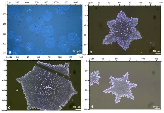
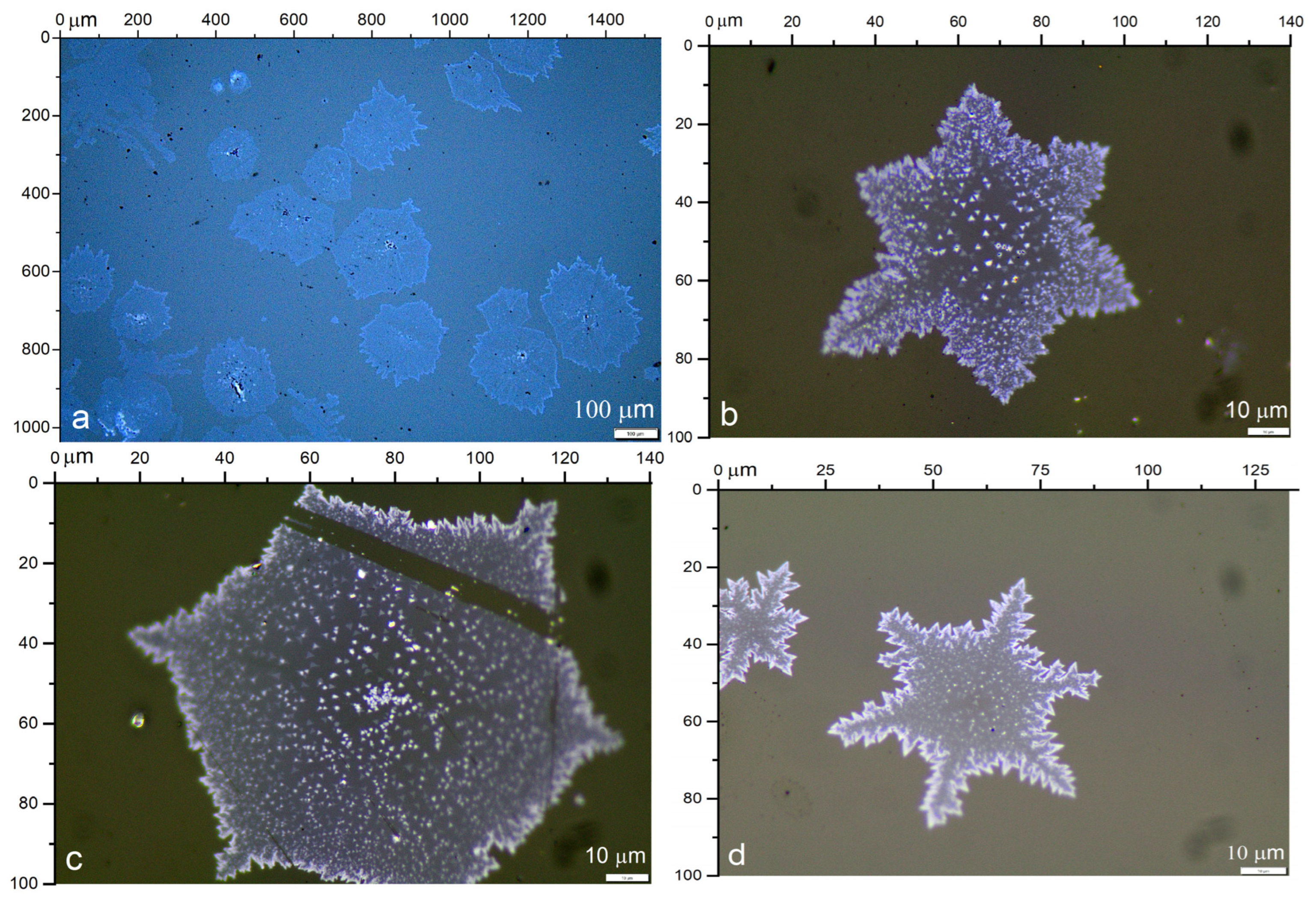
Through the mediation of the meta-tungstate, the WSe2 formation onto sapphire develops into polymorphic structures of various size, thickness and shapes. An optical microscopy gallery is presented in Figure 1a–d under different magnifications.
Figure 1.
Optical images of the largest polygonal WSe2 macroclusters (a) under reflected light and ×10 magnification. (b–d) Symmetrical star-like and hexagonal clusters under 100× magnification.
The major fraction consists of polygonal domains with multifaceted “saw-tooth” [31] edges. Their lateral dimensions can reach a typical macroscopic size up even to several hundreds of µm as shown under ×10 magnification in Figure 1a. Symmetrical hexagonal, star-like forms are also observed and a few representative clusters are presented in Figure 1b–d. The optical images under the highest magnification (×100) show sharp contrast differences for the thicker structure of the jagged peripheries.
Usually, the morphological disorder at the flake edges results from the imbalance between the growth dynamics of the deposited W-precursor and the rate of Se-diffusion [32]. Another factor leading to formation of irregular cluster boundaries is related to the particular edge-absorption of Na-based mediator complexes which is specific to salt-assisted liquid precursor deposition [15,33].
The miscellaneous cluster geometries of the TMDC materials have peculiar properties and practical functionalities [34,35]. These can be further developed towards specific shape and morphology engineering determined by the syntheses. For instance, the atypical fractal [36], dendritic [37], coralloid [38] and flower-like [39] patterns (similar to those observed in our study) show notable application potential, specifically in cases where the higher structural complexity [40] and edge irregularity [41] are favorable and lead to improved performance for electrocatalysis, hydrogen evolution reaction [40] and humidity-sensitive processes [42].
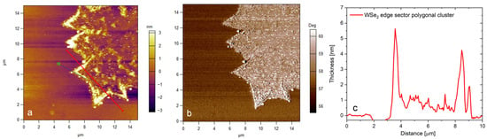
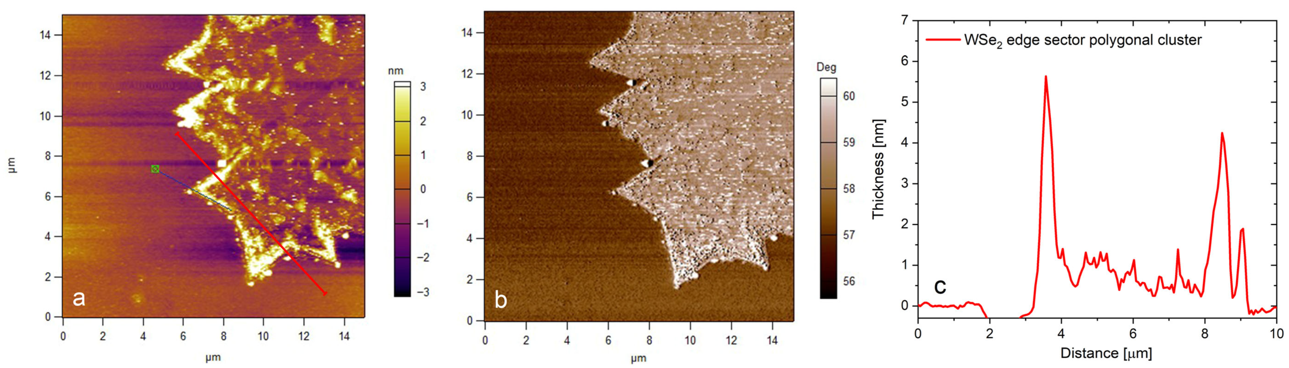
The interior of the polygonal formations also shows complex intergrowth consisting of densely positioned triangular islands. These are possibly formed due to coalescence of separate nucleation sites. This is probably a result of non-uniform molten precursor concentrations at the vapor–liquid–solid interfaces and locally variable Se-diffusion [43]. The thickness profiles and the nanomorphology of the large WSe2 polygonal cluster are identified by AFM. Selected topographical scans of local “saw-tooth” edge sectors are shown in Figure 2. The presented data includes both the nanometric thickness map (a) and the tapping mode phase (b) variations to highlight the growth features.
Figure 2.
2D maps of (a) AFM height, (b) phase contrast retraces and (c) thickness profile of WSe2 cluster.
The detected height profile (c) is in the 1–5 nm range, marking a mixed multilayered and single-layer structure of the WSe2 clusters. The multilayered WSe2 structures also show technologically promising valleytronic [44] and memristive [45] functionalities. In addition, WSe2 multilayer/monolayer homojunction structures (achieved with a similar approach) demonstrate semiconducting ambipolar characteristics and a p-n interface with diode rectification [46]. The observed surface irregularity of the relief also suggests uneven precursor deposition and/or rapid crystallization during the cluster formation.
The integral chemical composition (over a large area of the substrate) of meta-tungstate-synthesized WSe2 was analyzed by means of XPS. This is a powerful surface-sensitive method used for quantitative elemental and stoichiometric identification based on the analysis of sample’s chemical bond types and corresponding binding energy spectrum.
XPS probing penetration depth is on the order of 10 nanometers, which makes it especially suitable for characterization of nanostructured samples and ultra-thin films.
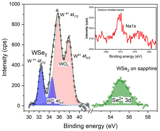
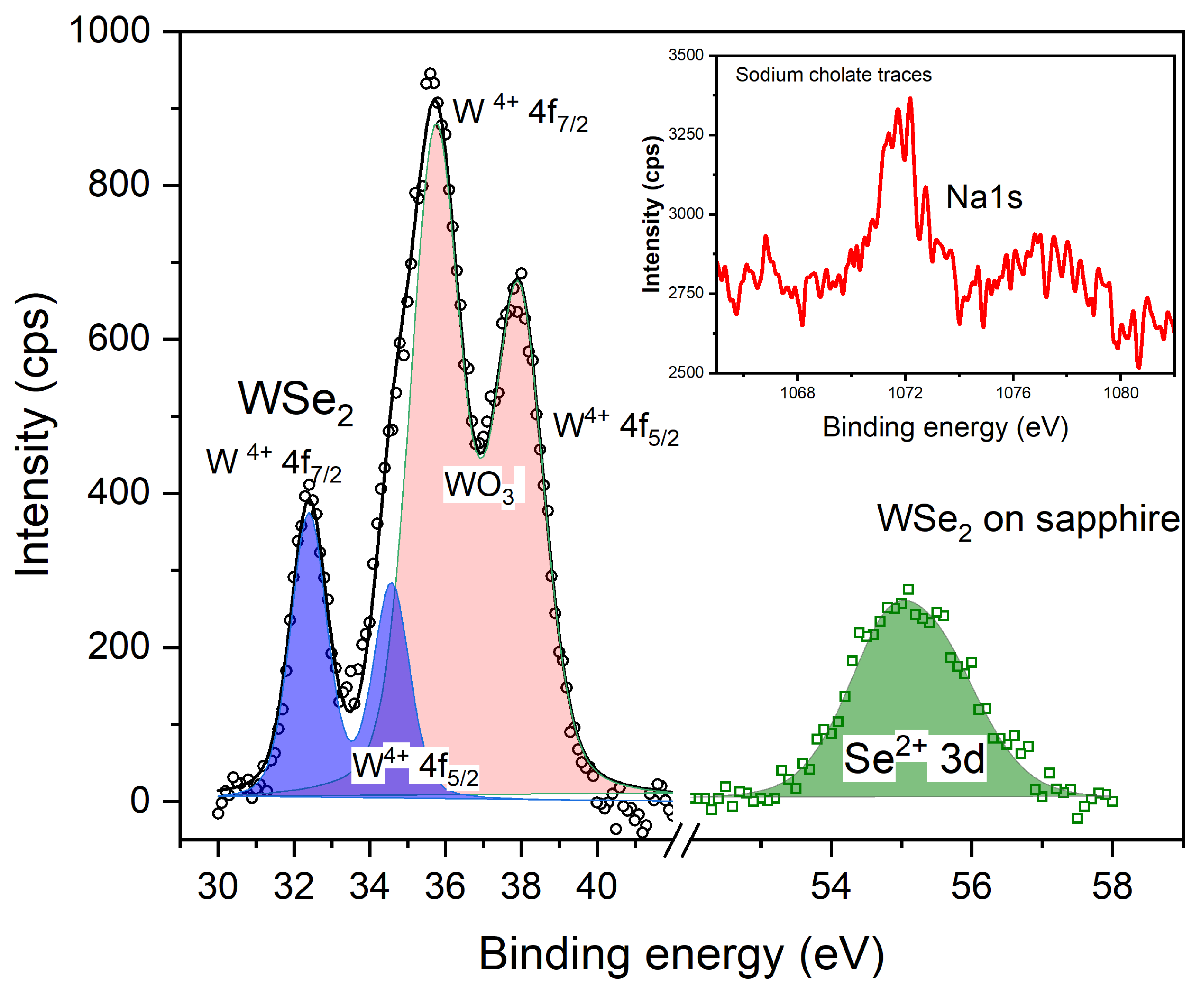
The acquired XPS spectra for the meta-tungstate WSe2 on sapphire is presented in Figure 3. The peak binding energy positions for both W and Se are consistent to similar studies reported in the literature [47]. The dataset uses 70% Gaussian, 30% Lorentzian fit following a simple procedure with Shirley background subtraction. The typical WSe2 strong electron-orbital degeneracy leads to splitting of the characteristic W4f states. The identified doublets correspond to W4f7/2 (binding energy = 32.4 eV) and W4f5/2 levels (binding energy = 34.5 eV). The second-strongest doublet in the same region W4f7/2 (35.7 eV) and W4f5/2 (37.9 eV) belongs to formation of WO3 oxide marking remnant precursor traces due to an incomplete selenization process. The Se-deficiency is also a factor for the increased edge and vertical morphology irregularities, formation of dendritic and fractal shapes [48] and clusterization, as observed in the optical images and AFM profiles.
Figure 3.
XPS spectra of W 4f and Se 3d binding energies for WSe2. The inset graph shows Na1s minor traces related to the SC.
The XPS peak deconvolution of W4f region provides an estimation of the chemical phase proportion of WSe2 (30%)/WO3 (70%). It can be noted that the formation of both WSe2/WO3 also has certain practical prospects since their interaction facilitates charge trapping and transfer processes [49] which are fundamental for resistive-switching memristive applications. The Se 3d (Se 3d5/2 and Se 3d3/2) peak has overlapping spin–orbit components (Δ = 0.86 eV), and are undistinguished for the spectral resolution of the instrument. We should point out here that in the same region a W 5p3/2 peak appears at around 37.9 eV (not included in the fit because its contribution is insignificant) for the first doublet and for the second that is associated with the oxide it is outside of the main W4f envelope. There is also a characteristic peak associated with minimal residual trace of Na from the dissolved sodium cholate (Figure 3 inset).
Raman spectroscopy is universally applied for crystal structure characterization of 2D materials, especially for identification of the layer number, electronic band and charge carrier effects, chemical (doping) and structural (strain) modifications, interlayer coupling, etc. [50,51,52,53]. The archetypical Raman spectra for 2D TMDC are characterized by two first-order modes: E2g—caused by the in-plane oscillations of both chalcogenide and transition metal atoms—and the A1g mode related to out-of-plane vibrations of the chalcogenide atom sub-lattice.
The Raman spectrum of WSe2 is specific and the complete interpretation and assignment of the phonon structure and dynamics is still in progress [54]. There are several unique spectral signatures with complex overlapping of both first and multiple second-order bands. A general overview of the relevant peak tendencies as spectral shifts and changes in the intensity also enable an indirect assessment of WSe2 layer numbers. The specific details are outlined below [55,56]:
- -
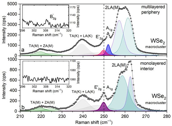
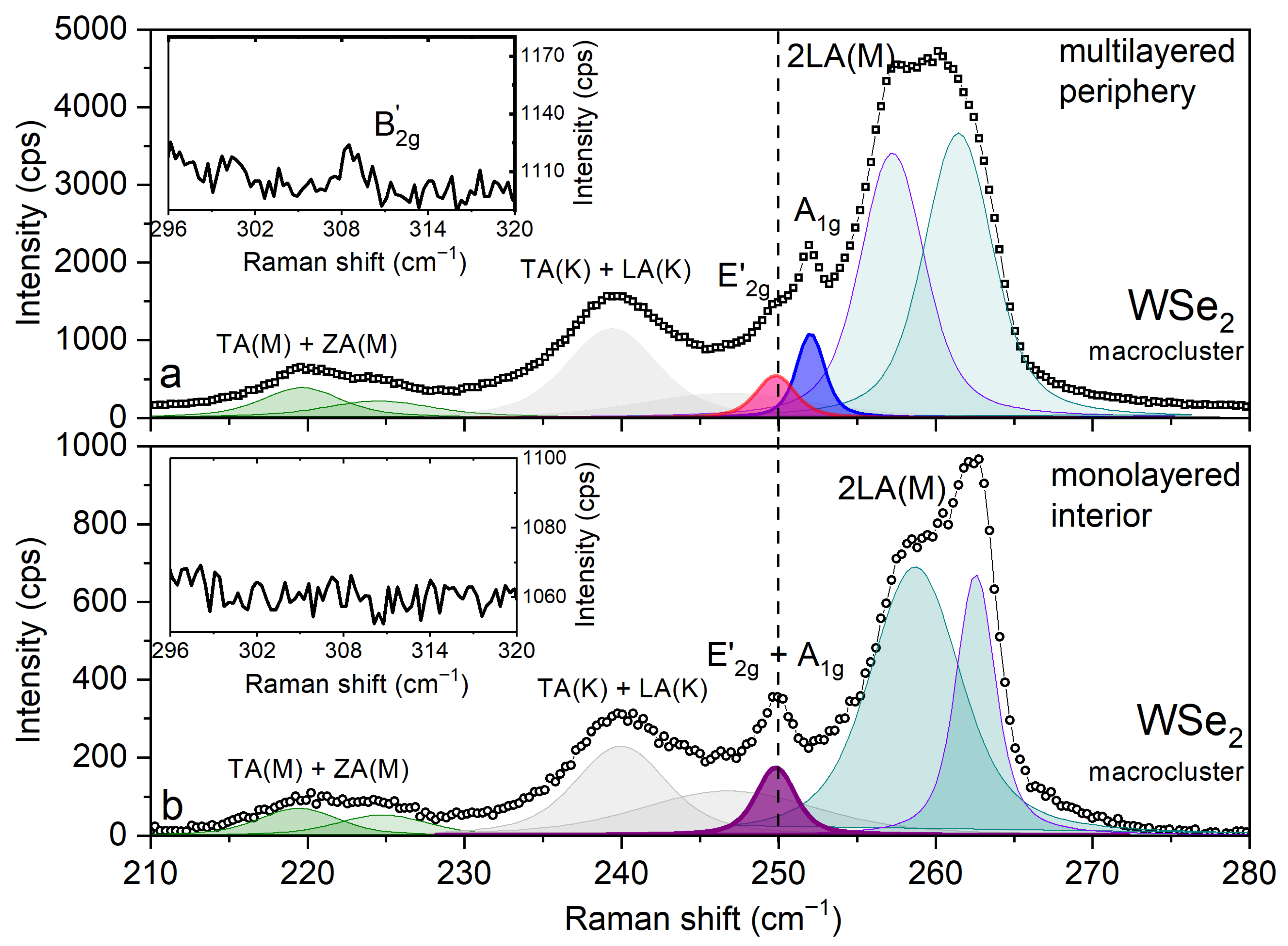
- The first-order Raman modes (E2g and A1g) are very close in frequency. For the single-atomic layer the corresponding phonon states are quasi degenerate and both peaks almost coincide in close proximity to 250 cm−1 [53]. With increasing of the layer numbers, the characteristic A1g and E2g modes exhibit opposite shifts and a good example for the separation is clearly visible in the deconvoluted spectra in Figure 4 for the investigated multilayered periphery of the WSe2 cluster.Figure 4. Deconvoluted Raman spectra of periphery (a) and interior (b) sector of part of WSe2 macrocluster with corresponding main peak identification. The inset graphs show enlarged view of the spectral interval with present/absent B2g.
- -
- The second-order phonon modes have a strong contribution all over the spectrum due to the enhancement effect of resonance Raman processes, especially when the laser excitation wavelength (in our case 633 nm/1.96 eV) is close to the specific (excitonic) inter-band transitions in the WSe2 electronic structure.
- -
- The most prominent resonant band is located around 260 cm−1 marking LA phonon overtone at the M point in the Brillouin zone (designated as 2LA(M)) and A(M) phonon activated by structural disorder (especially intense at 633 nm laser excitation). As this band principally undergoes a downshift upon WSe2 thickness increase [50,51,52,53], the observed splitting effects and spectral-weight shift within this band from Figure 4a to Figure 4b reflect the mixed multilayer/monolayer morphology of the examined WSe2 cluster.
The deconvoluted Raman spectra of the large WSe2 polygonal formations on sapphire are presented comparatively in Figure 4a,b with scans taken from different cluster positions: edge area and interior area. We observe previously noted thickness-sensitive spectral variations: the variable position and intensity change of the E2g peak and A1g peak along with prominent blue-shift of spectral weight within the second-order 2LA(M) band in the spectral interval around 260 cm−1. As noted for multilayer WSe2, E2g and A1g are well separated in frequency, while for monolayer they are virtually degenerate at 250 cm−1 and accordingly are both fitted with a common single peak. For the deconvolution of the main Raman band between 200 and 300 cm−1, several Voigt profiles are used to fit the second-order features and the first-order Raman active phonons (the 2LA(M) band was fitted with a two-peak combination).
The peaks for the Raman phonons are plotted with thicker traces. The data reveal the few-layer structure (separated E2g and A1g) in the periphery regions and a monolayer (both E2g and A1g in vicinity of 250 cm−1) in the interior of the WSe2 cluster in accordance with the AFM results in Figure 2a–c. Another typical signature of the multilayer van der Waals interactions in WSe2 is demonstrated by the appearance of the forbidden peak B2g close to 308 cm−1 caused by the vertical W-Se bond modulation (inset a) [50,51,52,53,55]. In comparison, B2g peak is absent in the Raman spectra of the cluster’s interior (inset b).
4. Conclusions
In this study we have presented a structural, chemical, morphological and spectral analysis on liquid-precursor-mediated CVD (ambient pressure and moderate temperatures) synthesis of WSe2 onto sapphire as an extension to the data published in a previous work [1].
The structural and surface quality of the sapphire substrate provide favorable conditions for CVD synthesis of large-size WSe2 domains. The following concluding remarks can be outlined:
- The predominant WSe2 macrocluster formations with random shapes and saw-tooth periphery can reach sizes up to several hundred micrometers. Large symmetrical hexagonal and/or polygonal star-like forms were also observed. To the best of our knowledge, the obtained structures are unique in terms of size, geometry and coverage when compared to the available studies using different variants of the liquid-precursor-mediated synthesis or the conventional CVD approaches.
- The XPS analysis verified the successful WSe2 formation with a significant amount of WO3 that belongs to still-incomplete selenization and minor residual traces from the growth promoter remained under the applied moderate thermal regime (TCVD ~710 °C).
- The Raman spectroscopy identified a mixed multilayer/monolayer morphology of the investigated polygonal macroclusters, also in accordance with the AFM results. The Raman spectra also show several unique features such as complex peak structure with remarkable splitting effects and spectral-weight shifts within the intense second-order 2LA(M) band related to excitonic-resonance processes. In this aspect, the analysis of the observed spectral behavior yields a valuable contribution to the Raman characterization methodology and database for WSe2 micro- and nanoclusters with variable thickness.
The presented data provide a base for further stages for improvement and development of liquid-precursor-mediated CVD synthesis of WSe2 onto sapphire and the numerous optical functionalities of both materials open many practical directions for opto-electronic applications.
Author Contributions
Conceptualization, K.B., P.R., V.M. and D.D.; methodology, K.B., P.R., I.A., N.M., V.V., V.S., T.L., D.D. and V.M.; software, K.B.; validation, K.B., P.R. and I.A.; formal analysis, K.B. and P.R.; investigation, K.B., P.R., I.A., N.M., V.V., V.S., T.L., D.D. and V.M.; resources, D.D., V.M. and P.R.; data curation, K.B.; writing—original draft preparation, K.B.; writing—review and editing, K.B., V.M., D.D. and P.R.; visualization, K.B.; supervision, D.D. and V.M.; project administration, D.D. and V.M.; funding acquisition, D.D. and V.M. All authors have read and agreed to the published version of the manuscript.
Funding
We acknowledge the Bulgarian Science Fund support under the project number KП-06-H 98/7 and FNI KП-06 KOCT/24 under the COST Action CA22123 European Materials Acceleration Center for Energy (EU-MACE). Financial support from the Research equipment of distributed research infrastructure INFRAMAT (part of Bulgarian national roadmap for research infrastructures) supported by the Bulgarian Ministry of Education and Science is also acknowledged. This work was supported by the European Regional Development Fund under the “Research Innovation and Digitization for Smart Transformation” program 2021–2027 under Project BG16RFPR002-1.014-0006 “National Centre of Excellence Mechatronics and Clean Technologies”.
Data Availability Statement
Dataset available on request from the authors.
Conflicts of Interest
The authors declare no conflicts of interest.
References
- Buchkov, K.; Rafailov, P.; Minev, N.; Videva, V.; Strijkova, V.; Lukanov, T.; Dimitrov, D.; Marinova, V. Metatungstate Chemical Vapor Deposition of WSe2: Substrate Effects, Shapes, and Morphologies. Crystals 2024, 14, 184. [Google Scholar] [CrossRef] [Scilit]
- Mohl, M.; Rautio, A.-R.; Asres, G.A.; Wasala, M.; Patil, P.D.; Talapatra, S.; Kordas, K. 2D Tungsten Chalcogenides: Synthesis, Properties and Applications. Adv. Mater. Interfaces 2020, 7, 2000002. [Google Scholar] [CrossRef] [Scilit]
- Eftekhari, A. Tungsten Dichalcogenides (WS2, WSe2, and WTe2): Materials Chemistry and Applications. J. Mater. Chem. A 2017, 5, 18299–18325. [Google Scholar] [CrossRef] [Scilit]
- Cheng, Q.; Pang, J.J.; Sun, D.; Wang, J.J.; Zhang, S.; Liu, F.; Chen, Y.; Yang, R.; Liang, N.; Lu, X.; et al. WSe2 2D P-Type Semiconductor-Based Electronic Devices for Information Technology: Design, Preparation, and Applications. InfoMat 2020, 2, 656–697. [Google Scholar] [CrossRef] [Scilit]
- Yao, Z.; Liu, J.; Xu, K.; Chow, E.K.C.C.; Zhu, W. Material Synthesis and Device Aspects of Monolayer Tungsten Diselenide. Sci. Rep. 2018, 8, 5221. [Google Scholar] [CrossRef] [Scilit]
- Xu, S.; Shen, J.; Long, G.; Wu, Z.; Bao, Z.Q.; Liu, C.C.; Xiao, X.; Han, T.; Lin, J.; Wu, Y.; et al. Odd-Integer Quantum Hall States and Giant Spin Susceptibility in p-Type Few-Layer WSe2. Phys. Rev. Lett. 2017, 118, 067702. [Google Scholar] [CrossRef] [Scilit]
- Courtade, E.; Semina, M.; Manca, M.; Glazov, M.M.; Robert, C.; Cadiz, F.; Wang, G.; Taniguchi, T.; Watanabe, K.; Pierre, M.; et al. Charged Excitons in Monolayer WSe2: Experiment and Theory. Phys. Rev. B 2017, 96, 085302. [Google Scholar] [CrossRef] [Scilit]
- Wang, J.; Xie, F.; Cao, X.H.; An, S.C.; Zhou, W.X.; Tang, L.M.; Chen, K.Q. Excellent Thermoelectric Properties in Monolayer WSe2 Nanoribbons Due to Ultralow Phonon Thermal Conductivity. Sci. Rep. 2017, 7, 41418. [Google Scholar] [CrossRef] [Scilit]
- Sortino, L.; Zotev, P.G.; Phillips, C.L.; Brash, A.J.; Cambiasso, J.; Marensi, E.; Fox, A.M.; Maier, S.A.; Sapienza, R.; Tartakovskii, A.I. Bright Single Photon Emitters with Enhanced Quantum Efficiency in a Two-Dimensional Semiconductor Coupled with Dielectric Nano-Antennas. Nat. Commun. 2021, 12, 6063. [Google Scholar] [CrossRef] [Scilit]
- Sierra, J.F.; Fabian, J.; Kawakami, R.K.; Roche, S.; Valenzuela, S.O. Van Der Waals Heterostructures for Spintronics and Opto-Spintronics. Nat. Nanotechnol. 2021, 16, 856–868. [Google Scholar] [CrossRef] [Scilit]
- Zhao, S.; Li, X.; Dong, B.; Wang, H.; Wang, H.; Zhang, Y.; Han, Z.; Zhang, H. Valley Manipulation in Monolayer Transition Metal Dichalcogenides and Their Hybrid Systems: Status and Challenges. Rep. Prog. Phys. 2021, 84, 026401. [Google Scholar] [CrossRef] [Scilit]
- Xia, Y.; Han, Z.; Watanabe, K.; Taniguchi, T.; Shan, J.; Mak, K.F. Superconductivity in Twisted Bilayer WSe2. Nature 2025, 637, 833–838. [Google Scholar] [CrossRef] [Scilit]
- Srivastava, A.; Sidler, M.; Allain, A.V.; Lembke, D.S.; Kis, A.; Imamoglu, A. Optically Active Quantum Dots in Monolayer WSe2. Nat. Nanotechnol. 2015, 10, 491–496. [Google Scholar] [CrossRef] [Scilit]
- Wang, Z.; Wang, W.; Liu, P.; Liu, G.; Li, J.; Zhao, J.; Zhou, Z.; Wang, J.; Pei, Y.; Zhao, Z.; et al. Superlow Power Consumption Artificial Synapses Based on WSe2 Quantum Dots Memristor for Neuromorphic Computing. Research 2022, 2022, 9754876. [Google Scholar] [CrossRef] [Scilit]
- Wu, J.; Zhang, Y.; Jia, Z.; Ma, Z.; Song, J. Study on the Morphological Mechanism of MoS2 Growth by NaCl-Assisted Chemical Vapor Deposition. ChemistrySelect 2023, 8, e202301599. [Google Scholar] [CrossRef] [Scilit]
- Cai, Z.; Liu, B.; Zou, X.; Cheng, H.M. Chemical Vapor Deposition Growth and Applications of Two-Dimensional Materials and Their Heterostructures. Chem. Rev. 2018, 118, 6091–6133. [Google Scholar] [CrossRef] [Scilit]
- Tang, L.; Tan, J.; Nong, H.; Liu, B.; Cheng, H.-M. Chemical Vapor Deposition Growth of Two-Dimensional Compound Materials: Controllability, Material Quality, and Growth Mechanism. Acc. Mater. Res. 2020, 2, 36–47. [Google Scholar] [CrossRef] [Scilit]
- Liu, J.; Zeng, M.; Wang, L.; Chen, Y.; Xing, Z.; Zhang, T.; Liu, Z.; Zuo, J.; Nan, F.; Mendes, R.G.; et al. Ultrafast Self-Limited Growth of Strictly Monolayer WSe2 Crystals. Small 2016, 12, 5741–5749. [Google Scholar] [CrossRef] [Scilit] [PubMed]
- Xie, C.; Yang, P.; Huan, Y.; Cui, F.; Zhang, Y. Roles of Salts in the Chemical Vapor Deposition Synthesis of Two-Dimensional Transition Metal Chalcogenides. Dalton Trans. 2020, 49, 10319–10327. [Google Scholar] [CrossRef] [Scilit]
- Wong, S.L.; Liu, H.; Chi, D. Recent Progress in Chemical Vapor Deposition Growth of Two-Dimensional Transition Metal Dichalcogenides. Prog. Cryst. Growth Charact. Mater. 2016, 62, 9–28. [Google Scholar] [CrossRef] [Scilit]
- You, J.; Hossain, M.D.; Luo, Z. Synthesis of 2D Transition Metal Dichalcogenides by Chemical Vapor Deposition with Controlled Layer Number and Morphology. Nano Converg. 2018, 5, 26. [Google Scholar] [CrossRef] [Scilit]
- Li, S. Salt-Assisted Chemical Vapor Deposition of Two-Dimensional Transition Metal Dichalcogenides. iScience 2021, 24, 103229. [Google Scholar] [CrossRef] [Scilit]
- Guan, H.; Zhao, B.; Zhao, W.; Ni, Z. Liquid-Precursor-Intermediated Synthesis of Atomically Thin Transition Metal Dichalcogenides. Mater. Horiz. 2023, 10, 1105–1120. [Google Scholar] [CrossRef] [Scilit] [PubMed]
- Seo, J.; Lee, J.; Baek, S.; Jung, W.; Oh, N.K.; Son, E.; Park, H. Liquid Precursor-Mediated Epitaxial Growth of Highly Oriented 2D van Der Waals Semiconductors toward High-Performance Electronics. ACS Appl. Electron. Mater. 2021, 3, 5528–5536. [Google Scholar] [CrossRef] [Scilit]
- Shen, D.; Jin, Y.; Zhang, Z.; Song, R.; Liu, M.; Li, W.; Li, X.; Wu, R.; Li, B.; Li, J.; et al. Recent Advances in Spin-Coating Precursor Mediated Chemical Vapor Deposition of Two-Dimensional Transition Metal Dichalcogenides. Precis. Chem. 2024, 2, 282–299. [Google Scholar] [CrossRef] [Scilit]
- Lee, Y.; Shin, N. Mechanistic Insights into Diffusion-Controlled 2D WSe2 Growth via Chemical Vapor Deposition in Confined Spaces. FlatChem 2025, 51, 100863. [Google Scholar] [CrossRef] [Scilit]
- Alahmadi, M.; Mahvash, F.; Szkopek, T.; Siaj, M. A Two-Step Chemical Vapor Deposition Process for the Growth of Continuous Vertical Heterostructure WSe2/h-BN and Its Optical Properties. RSC Adv. 2021, 11, 16962–16969. [Google Scholar] [CrossRef] [Scilit]
- Zhang, X.; Choudhury, T.H.; Chubarov, M.; Xiang, Y.; Jariwala, B.; Zhang, F.; Alem, N.; Wang, G.C.; Robinson, J.A.; Redwing, J.M. Diffusion-Controlled Epitaxy of Large Area Coalesced WSe2 Monolayers on Sapphire. Nano Lett. 2018, 18, 1049–1056. [Google Scholar] [CrossRef] [Scilit]
- Han, A.; Aljarb, A.; Liu, S.; Li, P.; Ma, C.; Xue, F.; Lopatin, S.; Yang, C.W.; Huang, J.K.; Wan, Y.; et al. Growth of 2H Stacked WSe2 Bilayers on Sapphire. Nanoscale Horiz. 2019, 4, 1434–1442. [Google Scholar] [CrossRef] [Scilit]
- Chen, L.; Liu, B.; Ge, M.; Ma, Y.; Abbas, A.N.; Zhou, C. Step-Edge-Guided Nucleation and Growth of Aligned WSe2 on Sapphire via a Layer-over-Layer Growth Mode. ACS Nano 2015, 9, 8368–8375. [Google Scholar] [CrossRef] [Scilit]
- Cai, L.; Shearer, M.J.; Zhao, Y.; Hu, Z.; Wang, F.; Zhang, Y.; Eliceiri, K.W.; Hamers, R.J.; Yan, W.; Wei, S.; et al. Chemically Derived Kirigami of WSe2. J. Am. Chem. Soc. 2018, 140, 10980–10987. [Google Scholar] [CrossRef] [Scilit] [PubMed]
- Dziobek-Garrett, R.; Hilliard, S.; Sriramineni, S.; Ambrozaite, O.; Zhu, Y.; Hudak, B.M.; Brintlinger, T.H.; Chowdhury, T.; Kempa, T.J. Controlling Morphology and Excitonic Disorder in Monolayer WSe2 Grown by Salt-Assisted CVD Methods. ACS Nanosci. Au 2023, 3, 441–450. [Google Scholar] [CrossRef] [Scilit]
- Lee, J.; Shin, N. Toward an Understanding of the Mechanism of Mixed-Salt-Mediated CVD Growth of MoSe2. Appl. Phys. Lett. 2023, 123, 181902. [Google Scholar] [CrossRef] [Scilit]
- Basu, P.; Chatterjee, K. Engineering of Layered Metal Dichalcogenides: Introducing Imperfections to Make It Perfect. Oxf. Open Mater. Sci. 2020, 1, itab012. [Google Scholar] [CrossRef] [Scilit]
- Lv, R.; Terrones, H.; Elías, A.L.; Perea-López, N.; Gutiérrez, H.R.; Cruz-Silva, E.; Rajukumar, L.P.; Dresselhaus, M.S.; Terrones, M. Two-Dimensional Transition Metal Dichalcogenides: Clusters, Ribbons, Sheets and More. Nano Today 2015, 10, 559–592. [Google Scholar] [CrossRef] [Scilit]
- Wang, P.; Luo, S.; Boyle, L.; Zeng, H.; Huang, S. Controlled Fractal Growth of Transition Metal Dichalcogenides. Nanoscale 2019, 11, 17065–17072. [Google Scholar] [CrossRef] [Scilit] [PubMed]
- Xu, W.; Li, S.; Zhou, S.; Lee, J.K.; Wang, S.; Sarwat, S.G.; Wang, X.; Bhaskaran, H.; Pasta, M.; Warner, J.H. Large Dendritic Monolayer MoS2 Grown by Atmospheric Pressure Chemical Vapor Deposition for Electrocatalysis. ACS Appl. Mater. Interfaces 2018, 10, 4630–4639. [Google Scholar] [CrossRef] [Scilit]
- Shao, G.; Xue, X.X.; Zhou, X.; Xu, J.; Jin, Y.; Qi, S.; Liu, N.; Duan, H.; Wang, S.; Li, S.; et al. Shape-Engineered Synthesis of Atomically Thin 1T-SnS2 Catalyzed by Potassium Halides. ACS Nano 2019, 13, 8265–8274. [Google Scholar] [CrossRef] [Scilit]
- Jiang, S.; Zhang, Z.; Zhang, N.; Huan, Y.; Gong, Y.; Sun, M.; Shi, J.; Xie, C.; Yang, P.; Fang, Q.; et al. Application of Chemical Vapor–Deposited Monolayer ReSe2 in the Electrocatalytic Hydrogen Evolution Reaction. Nano Res. 2018, 11, 1787–1797. [Google Scholar] [CrossRef] [Scilit]
- Wan, Y.; Zhang, Z.; Xu, X.; Zhang, Z.; Li, P.; Fang, X.; Zhang, K.; Yuan, K.; Liu, K.; Ran, G.; et al. Engineering Active Edge Sites of Fractal-Shaped Single-Layer MoS2 Catalysts for High-Efficiency Hydrogen Evolution. Nano Energy 2018, 51, 786–792. [Google Scholar] [CrossRef] [Scilit]
- Fu, W.; John, M.; Maddumapatabandi, T.D.; Bussolotti, F.; Yau, Y.S.; Lin, M.; Johnson Goh, K.E. Toward Edge Engineering of Two-Dimensional Layered Transition-Metal Dichalcogenides by Chemical Vapor Deposition. ACS Nano 2023, 17, 16348–16368. [Google Scholar] [CrossRef] [Scilit]
- Ren, J.; Guo, B.; Feng, Y.; Yu, K. Few-Layer MoS2 Dendrites as a Highly Active Humidity Sensor. Phys. E Low-Dimens. Syst. Nanostructures 2020, 116, 113782. [Google Scholar] [CrossRef] [Scilit]
- Chowdhury, S.; Roy, A.; Bodemann, I.; Banerjee, S.K. Two-Dimensional to Three-Dimensional Growth of Transition Metal Diselenides by Chemical Vapor Deposition: Interplay between Fractal, Dendritic, and Compact Morphologies. ACS Appl. Mater. Interfaces 2020, 12, 15885–15892. [Google Scholar] [CrossRef] [Scilit]
- Guan, H.; Tang, N.; Huang, H.; Zhang, X.; Su, M.; Liu, X.; Liao, L.; Ge, W.; Shen, B. Inversion Symmetry Breaking Induced Valley Hall Effect in Multilayer WSe2. ACS Nano 2019, 13, 9325–9331. [Google Scholar] [CrossRef] [Scilit]
- Shen, H.; Ren, J.; Li, J.; Chen, Y.; Lan, S.; Wang, J.; Wang, H.; Li, D. Multistate Memory Enabled by Interface Engineering Based on Multilayer Tungsten Diselenide. ACS Appl. Mater. Interfaces 2020, 12, 58428–58434. [Google Scholar] [CrossRef] [Scilit]
- Mandyam, S.V.; Zhao, M.Q.; Masih Das, P.; Zhang, Q.; Price, C.C.; Gao, Z.; Shenoy, V.B.; Drndić, M.; Johnson, A.T.C. Controlled Growth of Large-Area Bilayer Tungsten Diselenides with Lateral P–N Junctions. ACS Nano 2019, 13, 10490–10498. [Google Scholar] [CrossRef] [Scilit]
- Jiang, D.; Wang, X.; Chen, R.; Sun, J.; Kang, H.; Ji, D.; Liu, Y.; Wei, D. Self-Expanding Molten Salt-Driven Growth of Patterned Transition-Metal Dichalcogenide Crystals. J. Am. Chem. Soc. 2022, 144, 8746–8755. [Google Scholar] [CrossRef] [Scilit] [PubMed]
- Tyagi, M.; Dey, S.; Sahoo, P.; Sahdev, D. Systematic Study of CVD-Growth Parameters in NaCl-Assisted Growth of MoSe2 Nanostructures: Nanoribbons, Dendrites and Spirals. Mater. Adv. 2025, 6, 4833–4846. [Google Scholar] [CrossRef] [Scilit]
- Sivan, M.; Li, Y.; Veluri, H.; Zhao, Y.; Tang, B.; Wang, X.; Zamburg, E.; Leong, J.F.; Niu, J.X.; Chand, U.; et al. All WSe2 1T1R Resistive RAM Cell for Future Monolithic 3D Embedded Memory Integration. Nat. Commun. 2019, 10, 5201. [Google Scholar] [CrossRef] [Scilit]
- Shi, W.; Lin, M.L.; Tan, Q.H.; Qiao, X.F.; Zhang, J.; Tan, P.H. Raman and Photoluminescence Spectra of Two-Dimensional Nanocrystallites of Monolayer WS2 and WSe2. 2D Mater. 2016, 3, 025016. [Google Scholar] [CrossRef] [Scilit]
- Tonndorf, P.; Schmidt, R.; Böttger, P.; Zhang, X.; Börner, J.; Liebig, A.; Albrecht, M.; Kloc, C.; Gordan, O.; Zahn, D.R.T.; et al. Photoluminescence Emission and Raman Response of Monolayer MoS2, MoSe2, and WSe2. Opt. Express 2013, 21, 4908–4916. [Google Scholar] [CrossRef] [Scilit] [PubMed]
- Tangi, M.; Mishra, P.; Tseng, C.C.; Ng, T.K.; Hedhili, M.N.; Anjum, D.H.; Alias, M.S.; Wei, N.; Li, L.J.; Ooi, B.S. Band Alignment at GaN/Single-Layer WSe2 Interface. ACS Appl. Mater. Interfaces 2017, 9, 9110–9117. [Google Scholar] [CrossRef] [Scilit] [PubMed]
- Zhao, W.; Ghorannevis, Z.; Amara, K.K.; Pang, J.R.; Toh, M.; Zhang, X.; Kloc, C.; Tan, P.H.; Eda, G. Lattice Dynamics in Mono- and Few-Layer Sheets of WS2 and WSe2. Nanoscale 2013, 5, 9677–9683. [Google Scholar] [CrossRef] [Scilit]
- De Luca, M.; Cartoixà, X.; Martín-Sánchez, J.; López-Suárez, M.; Trotta, R.; Rurali, R.; Zardo, I. New Insights in the Lattice Dynamics of Monolayers, Bilayers, and Trilayers of WSe2 and Unambiguous Determination of Few-Layer-Flakes’ Thickness. 2D Mater. 2020, 7, 025004. [Google Scholar] [CrossRef] [Scilit]
- Terrones, H.; Del Corro, E.; Feng, S.; Poumirol, J.M.; Rhodes, D.; Smirnov, D.; Pradhan, N.R.; Lin, Z.; Nguyen, M.A.T.; Elías, A.L.; et al. New First Order Raman-Active Modes in Few Layered Transition Metal Dichalcogenides. Sci. Rep. 2014, 4, 4215. [Google Scholar] [CrossRef] [Scilit]
- Papanai, G.S.; Gupta, B.K. Spectroscopic Studies on CVD-Grown Monolayer, Bilayer, and Ribbon Structures of WSe2 Flakes. Mater. Chem. Front. 2023, 7, 3102–3115. [Google Scholar] [CrossRef] [Scilit]
Disclaimer/Publisher’s Note: The statements, opinions and data contained in all publications are solely those of the individual author(s) and contributor(s) and not of MDPI and/or the editor(s). MDPI and/or the editor(s) disclaim responsibility for any injury to people or property resulting from any ideas, methods, instructions or products referred to in the content. |
© 2026 by the authors. Licensee MDPI, Basel, Switzerland. This article is an open access article distributed under the terms and conditions of the Creative Commons Attribution (CC BY) license.