Article

Advancements in Complementary Metal-Oxide Semiconductor-Compatible Tunnel Barrier Engineered Charge-Trapping Synaptic Transistors for Bio-Inspired Neural Networks in Harsh Environments

1
Department of Electronic Materials Engineering, Kwangwoon University, Gwangun-ro 20, Nowon-gu, Seoul 01897, Republic of Korea
2
Department of Electronic Engineering, Kwangwoon University, Gwangun-ro 20, Nowon-gu, Seoul 01897, Republic of Korea
*
Author to whom correspondence should be addressed.
Biomimetics 2023, 8(6), 506; https://doi.org/10.3390/biomimetics8060506
Submission received: 17 August 2023 / Revised: 12 October 2023 / Accepted: 17 October 2023 / Published: 23 October 2023
(This article belongs to the Special Issue Bio-Inspired Neural Networks)

Abstract

:
This study aimed to propose a silicon-on-insulator (SOI)-based charge-trapping synaptic transistor with engineered tunnel barriers using high-k dielectrics for artificial synapse electronics capable of operating at high temperatures. The transistor employed sequential electron trapping and de-trapping in the charge storage medium, facilitating gradual modulation of the silicon channel conductance. The engineered tunnel barrier structure (SiO2/Si3N4/SiO2), coupled with the high-k charge-trapping layer of HfO2 and high-k blocking layer of Al2O3, enabled reliable long-term potentiation/depression behaviors within a short gate stimulus time (100 μs), even under elevated temperatures (75 and 125 °C). Conductance variability was determined by the number of gate stimuli reflected in the maximum excitatory postsynaptic current (EPSC) and the residual EPSC ratio. Moreover, we analyzed the Arrhenius relationship between the EPSC as a function of the gate pulse number (N = 1–100) and the measured temperatures (25, 75, and 125 °C), allowing us to deduce the charge trap activation energy. A learning simulation was performed to assess the pattern recognition capabilities of the neuromorphic computing system using the modified National Institute of Standards and Technology datasheets. This study demonstrates high-reliability silicon channel conductance modulation and proposes in-memory computing capabilities for artificial neural networks using SOI-based charge-trapping synaptic transistors.

1. Introduction

Synaptic devices have garnered considerable attention as potential replacements for conventional von Neumann computing architectures and Boolean logic [1,2]. Inspired by biological neurons and synapses in the human brain, synaptic devices are primarily used for artificial intelligence (AI) processing applications [3,4]. The fundamental roles of electrical synapses in brain-mimicking computing systems include massive parallelism, high operating speeds, low power consumption, and efficient storage/computation interconnection. Such systems demonstrate the capability of solving a wide range of problems in inference, recognition, optimization, and control [5,6].
Recently, diverse nonvolatile memory devices with various device structures and materials have been proposed for electronic synapses. In particular, two-terminal devices, such as phase-change and spintronic devices and memristors, have gained widespread attention owing to their potential for high integration in cross-array structures. However, these devices are susceptible to sneaking current issues and disturbances caused by excessive noise, necessitating additional control elements because of the structural connection between the stimulus and output domains [7,8]. In contrast, multiterminal synaptic transistors offer better suitability for complex neural computing functions and real-time processing owing to their independence from the stimulus/output domains. Multiterminal devices with various memory elements, such as floating-, electrolyte-, and ferroelectric-gate transistors, to implement synaptic behavior have been widely reported [9,10,11].
Meanwhile, the floating-gate device, a fundamental unit cell in modern flash memory, is rapidly approaching its intrinsic limits owing to its scaling down. Reducing the tunnel oxide thickness leads to inherent limitations in the scaling factors associated with floating-gate coupling, where the state of the adjacent cells is coupled via the gate leakage current and gate capacitance [12,13]. To address these challenges, charge trap flash (CTF) memory with advantageous structural attributes has emerged as an attractive candidate to ensure continuity in vertical scaling and overcome gate coupling limitations in conventional flash memory [14,15]. However, the SiO2/Si3N4/SiO2 structure in silicon–oxide–nitride–silicon (SONOS) presents fundamental issues in balancing data retention and erase speed. To enhance write and erase operations in SONOS memory, reducing the tunnel oxide thickness is essential [16,17,18]. On the other hand, maintaining a constant tunnel oxide thickness is crucial for long data retention to minimize leakage current problems caused by stress. To overcome the limitations of CTF-type nonvolatile memory, the use of high-k materials, such as zirconium, hafnium, tantalum, and aluminum oxides, in the tunneling and charge-trapping layers (CTLs) has been proposed to improve performance. These high-k materials exhibit relatively larger conduction band offsets with Si and higher dielectric constants and trap densities compared with conventional materials, resulting in superior charge-trapping characteristics [19,20,21].
In this study, we proposed a silicon-on-insulator (SOI)-based charge-trapping synaptic transistor with tunnel barrier engineering that utilizes high-k materials. The active application of charge trapping in nonvolatile memory devices has great potential for neural applications, offering high reliability, stable endurance, good data retention, and high fault tolerance [9]. Furthermore, its superior complementary metal-oxide semiconductor (CMOS) process compatibility enables ultrahigh device integration, making it a promising candidate for future artificial synaptic devices. We systematically evaluated the fundamental electrical properties and artificial neural behavior of the SOI-based charge-trapping synaptic transistors. Tunnel barrier engineering to enhance carrier injection by reducing the effective tunneling thickness is achieved via the ONO structure, where SiO2/Si3N4/SiO2 is laminated with a thin layer, and the HfO2 CTL and Al2O3 blocking layer (BL) are sequentially stacked to implement the charge-trapping synaptic transistor. By utilizing gate pulse stimuli, electrons are effectively trapped and de-trapped in a charge storage medium to mimic highly reliable synaptic action. The silicon channel conductance is gradually modulated via consecutive gate stimuli, and individual states are maintained for extended periods. This conductance variability is determined by the maximum excitatory-postsynaptic current (EPSC) and residual EPSC ratios, demonstrating a transition from short-term memory (STM) to long-term memory (LTM) mechanisms. We also evaluated the Arrhenius relationship between the EPSC and the number of gate pulse stimulations at measured temperatures (25, 75, and 125 °C) to gain insight into the trap activation energy (Ea). Moreover, the silicon channel conductance was successfully potentiated and depressed by short gate pulse stimuli (100 μs) during repeated endurance cycles at room temperature (25 °C) and even at high temperatures (75 and 125 °C). This highly reliable and discriminable conductance variability highlights the potential of SOI-based charge-trapping synaptic transistors for artificial neural network (ANN) systems. To demonstrate the performance of the proposed CMOS-compatible charge-trapping synaptic transistor in neuromorphic systems, we conducted recognition simulations using a modified National Institute of Standards and Technology (MNIST) dataset via a multilayer ANN model. The results exhibited high learning accuracy even at high temperatures, underscoring its potential as a viable component for neuromorphic computing and AI applications in harsh environments.

2. Materials and Methods

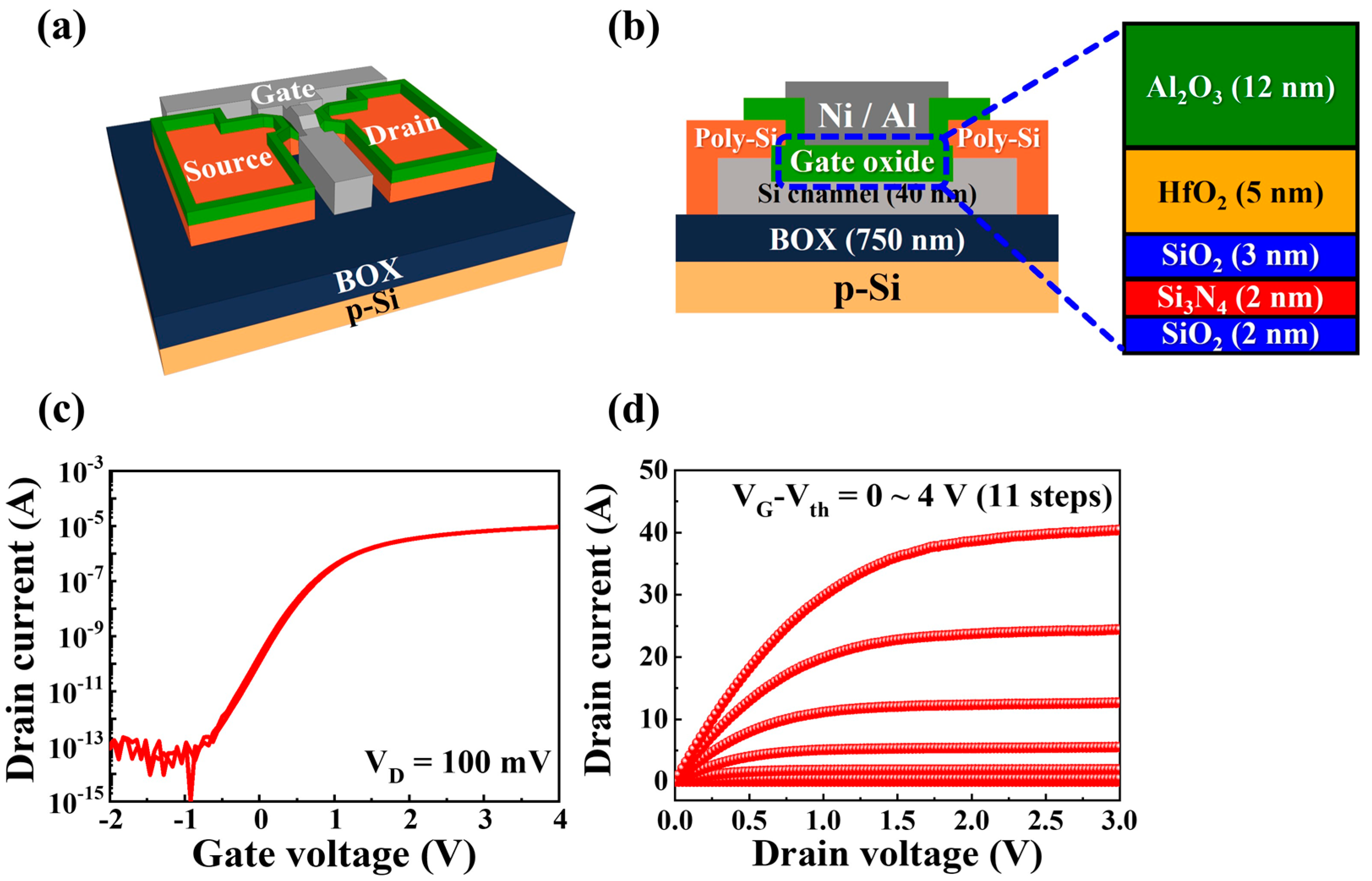
2.1. Fabrication of a Silicon-on-Insulator-Based Charge-Trapping Synaptic Transistor with Engineered Tunnel Barriers

The fabrication process for the charge-trapping synaptic transistors involves the utilization of (100) oriented p-type bonded and etch-back SOI wafers as the initial materials, followed by a standard Radio Corporation of America cleaning process to eliminate particles. The top silicon layer, with a doping concentration of 1 × 1015 cm−3, has a thickness of 100 nm, whereas the buried oxide layer measures 750 nm in thickness. The active regions of the top silicon undergo patterning using photolithography and are formed via CF4 reactive ion etching (RIE). Subsequently, a 100 nm thick in situ phosphorus-doped polysilicon layer is deposited for the source/drain (S/D) by employing a low-pressure chemical vapor deposition (LPCVD) process at 650 °C. Post-deposition annealing is performed via rapid thermal annealing at 850 °C for 30 s in an N2 ambient atmosphere. A 40 nm thick silicon channel layer with a low S/D series resistance is then achieved by RIE, which involves removing the n+-doped poly-Si layer (except for the S/D regions) and thinning the top silicon layer. Any surface damage and roughness on the silicon channel resulting from the thinning process are meticulously eliminated by treatment with an ammonia peroxide mixture solution. The channels are defined to have dimensions of 10 μm width and 10 μm length. The subsequent critical elements, engineered tunnel barriers CTL and BL, are established in the following sequence: A stack of ONO structures is deposited onto the silicon channel with layer thicknesses of 2 nm (SiO2, thermal oxidation), 2 nm (Si3N4, LPCVD), and 3 nm (SiO2, LPCVD), forming a variable oxide thickness (VARIOT) tunnel barrier. Subsequently, a 5 nm thick HfO2 film for the CTL and a 12 nm thick Al2O3 film for the BL is deposited using atomic layer deposition. The final step involves forming gas annealing at 450 °C in a 2% H2/N2 mixture at ambient temperature for 30 min following the deposition of a 20/100 nm thick Ni/Al gate electrode using an electron beam evaporator.

2.2. Characterizations

To ensure precise measurements and mitigate the effects of electrical noise and external light, CMOS-compatible charge-trapping synaptic transistors were placed within a shielded dark box on a probe station. The electrical characteristics of the proposed transistors were measured using an Agilent 4156 B Precision Semiconductor Parameter Analyzer (Hewlett-Packard Co., Palo Alto, CA, USA). Synaptic modulation was assessed by applying electrical pulse stimulation generated using an Agilent 8110A pulse generator (Hewlett-Packard Co.).

3. Results and Discussion

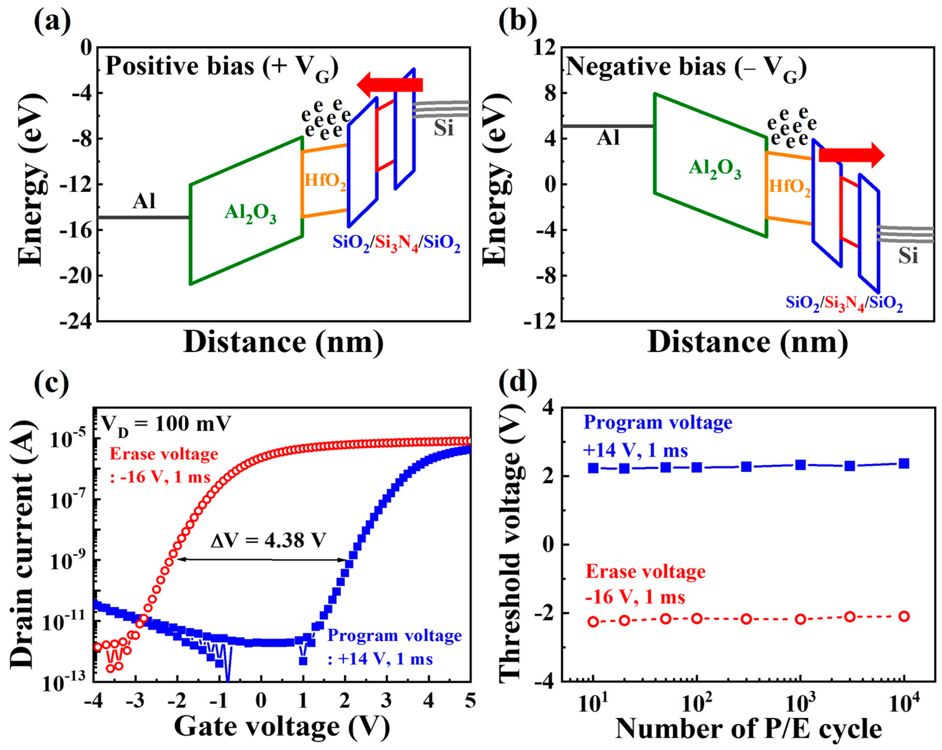
3.1. Electrical Characteristics of Complementary Metal-Oxide Semiconductor-Compatible Charge-Trapping Synaptic Transistors

Figure 1a,b present the schematics of the three-dimensional and vertical cross-sectional structures of the fabricated SOI-based charge-trapping synaptic transistor featuring an engineered tunnel barrier, known as the MAHONOS stack (gate metal/Al2O3/HfO2/SiO2/Si3N4/SiO2/Si), respectively. Figure 1c,d show the typical electrical characteristics of the transfer (ID-VG) and output (ID-VD) curves, respectively. In Figure 1c, the drain current (ID) is measured at a constant drain voltage (VD) of 100 mV while applying a gate voltage (VG) that ranges from −2 V to 4 V and then back to −2 V (VG sweep rate, 50 mV/step) for a dual-sweep operation. The threshold voltage (Vth) was extracted via linear extrapolation from the ID-VG curve in the linear region. Additionally, the hysteresis voltage (ΔVth) was defined as the difference between the forward sweep (Vthf) and backward sweep (Vthb), calculated as ΔVth = Vthf − Vthb. In Figure 1d, ID was measured as VG-Vth changes from 0 V to 4 V across 11 steps. The current linearly increased in the low VD region and subsequently pinched off as VD increased, resulting in saturation characteristics.
The electrical parameters of the SOI-based charge-trapping synaptic transistors were derived using the following equations [5,22]:
S S = d l o g I D d V G 1
and
μ F E = L g m W · C o x · V D , g m = I D V G
where W, L, Cox, and gm are the channel width, length, capacitance per unit area of the gate oxide, and transconductance, respectively. The extracted values for the Vth, on/off current ratio (Ion/Ioff), field-effect mobility (μFE), and subthreshold swing were approximately −0.09 V, 9.35 × 10⁷, 209.87 cm2/V∙s, and 204.52 mV/dec, respectively. Table 1 provides a summary of the electrical parameters extracted from the SOI-based charge-trapping synaptic transistors.
Figure 2a,b show the energy band diagrams of the MAHONOS stack under positive (VG > 0 V) and negative (VG < 0 V) gate bias conditions, respectively. In these diagrams, the Al2O3 layer serves as the BL, offering a high dielectric constant, a significantly large bandgap offset, and substantial physical oxide thickness (POT). The HfO2 layer was selected as the CTL because of its higher trap density, higher dielectric constant, and lower bandgap offset compared with the Al2O3 or SiO2 layers [23]. The engineered ONO structure, known as the VARIOT tunnel barrier, exhibits remarkable sensitivity to the electric field (E-field) generated by the gate bias [24]. When the energy of the electrons in the silicon channel is lower than that of the potential barrier, the thick ONO barrier prevents electron penetration. However, a substantial E-field causes significant band bending within the ONO barrier, allowing the electron wave function to tunnel through the thin triangular potential barrier [25]. Consequently, the channel conductance in the CTL can be modulated via charge trapping (resulting in a decrease in the conductance) or de-trapping (yielding an increase in the conductance). In retention mode, trapped charges remain stable in the CTL, and the charge-loss rate diminishes because of the substantial POT of the ONO barrier [26]. Figure 2c presents the transfer curve characteristics for the erase and program states. During programming, a gate bias of +14 V (for 1 ms) was applied, whereas erasing employed a bias of −16 V (for 1 ms). The threshold voltage shift attributed to charge trapping or de-trapping is approximately 4.38 V. Figure 2d shows the nonvolatile retention performance, demonstrating stable memory operation over 104 s based on the program/erase cycle counts. All Vth values remained unaltered during the 104-s observation period in both states.

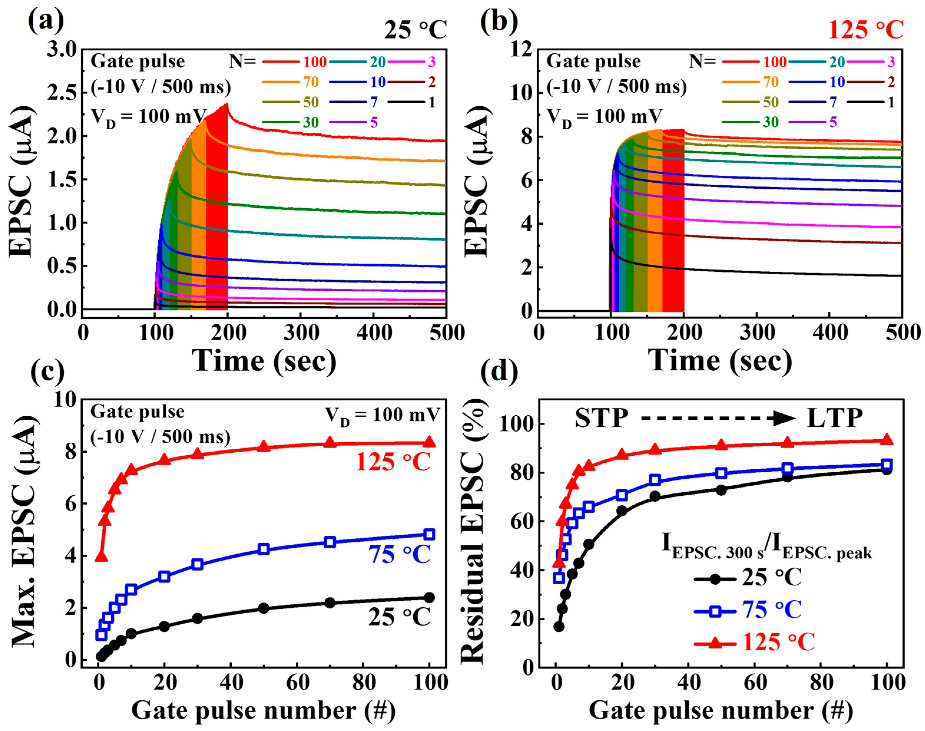
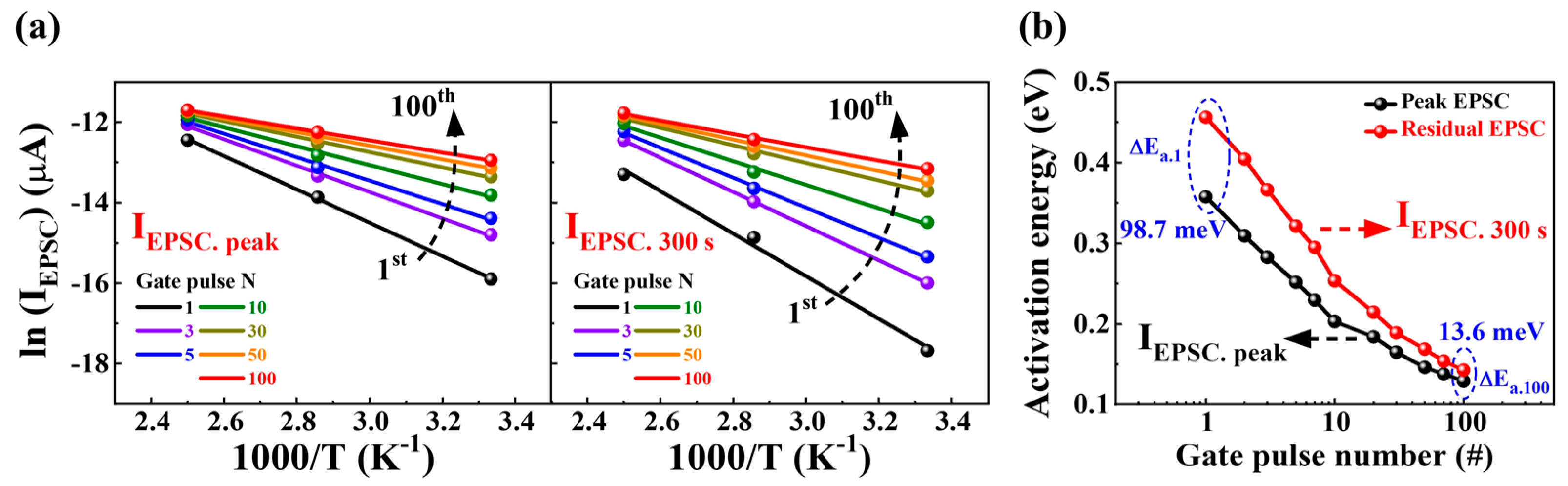
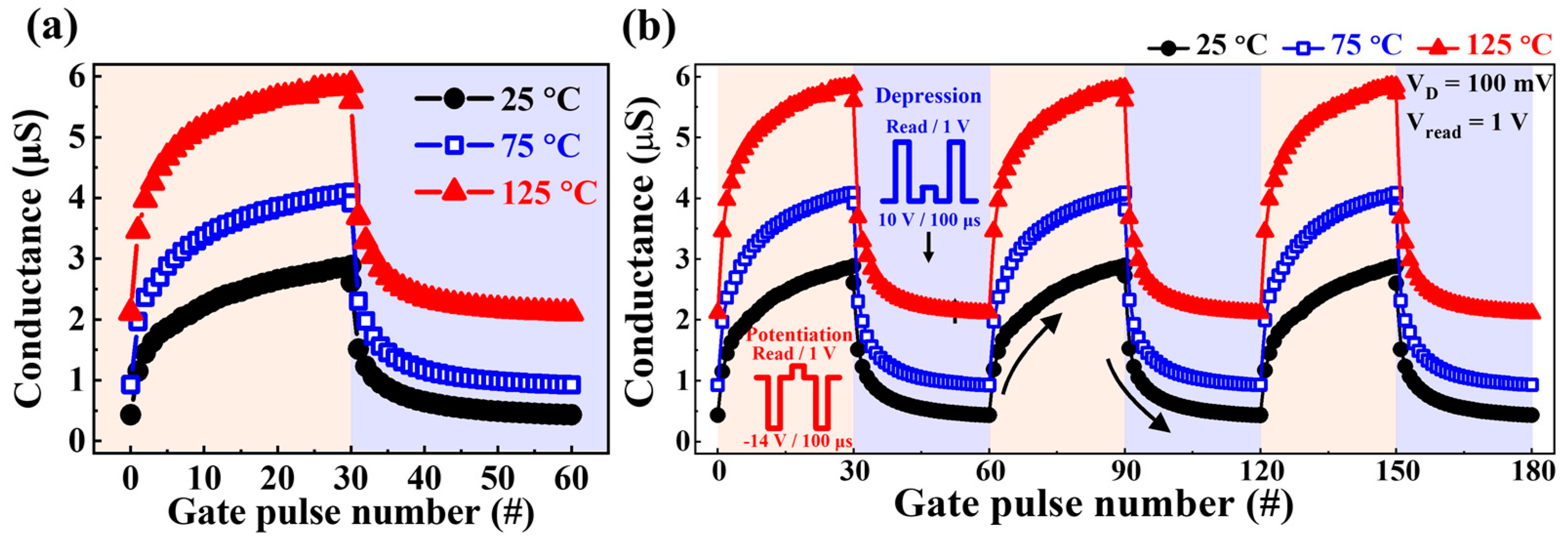
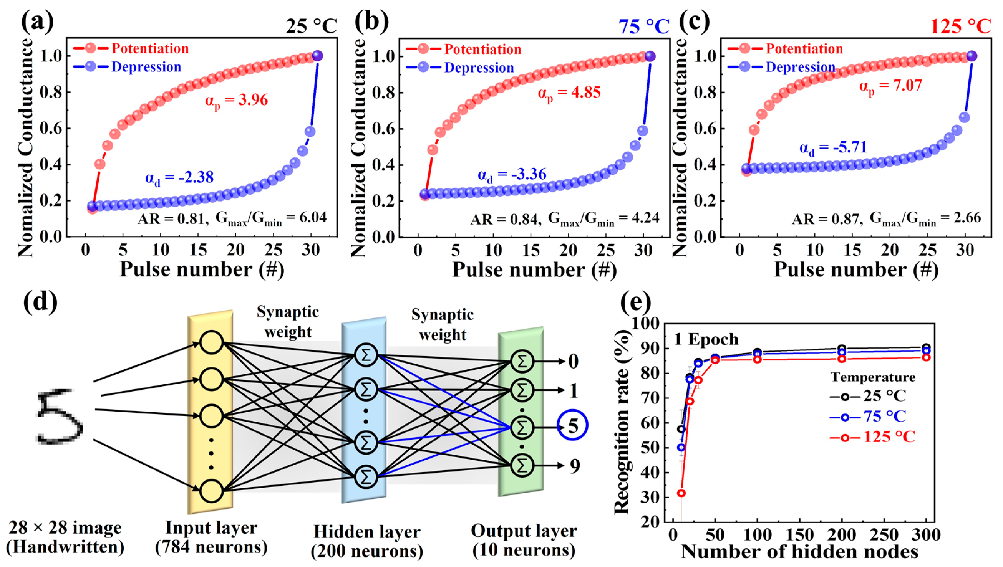
3.2. Synaptic Characteristics of CMOS-Compatible Charge-Trapping Synaptic Transistors

The operation of synaptic transistors, which are the fundamental computing engines in the human brain, is pivotal for emulating biological synaptic functions and mechanisms. In a synaptic transistor system, an additional gate electrode serves as the presynaptic terminal, and the drain current (ID) simulates the EPSC. As signals traverse presynaptic terminals, EPSCs synchronize via a specially functionalized gate oxide layer, thereby emulating neural actions [27,28].
Figure 3 shows the modulation of ID via controlled charge-trapping and charge-de-trapping dynamics in the CTL via an engineered ONO structure with a VARIOT tunneling barrier. This modulation was achieved by sequentially applying gate pulses. Positive or negative gate pulses caused differences in the barrier height within the E-field-sensitive VARIOT tunneling barrier, leading to charge trapping or de-trapping in the CTL via Fowler–Nordheim tunneling. Consequently, the channel conductance was gradually modulated based on the charge quantity within the CTL. Figure 3a illustrates the gradual trapping of electrons within the CTL via the consecutive application of N = 10 positive gate pulses (6 V/500 ms). Subsequently, ID sequentially decreased during the reading pulses at 0 V. Conversely, in Figure 3b, the application of 10 consecutive negative gate pulses (−10 V/500 ms) resulted in the gradual de-trapping of electrons within the CTL. Consequently, ID sequentially increased during the reading pulses at 0 V.
Electronic devices capable of operating in challenging high-temperature environments are crucial for control, computing, communication, surveillance, and reconnaissance. At elevated temperatures, the intrinsic carrier concentration (ni) of semiconductors is nonnegligible, which adds significance to neuromorphic AI systems for rapid automation and intelligent decision-making [29,30,31]. To comprehensively assess the reliable conductance modulation and temperature dependency of SOI-based charge-trapping synaptic transistors, we employed multiple gate pulses (N = 1–100) and measured the EPSC response under varying temperature conditions (25, 75, and 125 °C). Figure 4a,b illustrate typical EPSC responses as a function of gate pulse number (N = 1–100) at 25 and 125 °C, respectively. As the gate pulse numbers increased, the trapped charges within the CTL progressively de-trapped, resulting in a gradual increase in the EPSC. Notably, the individual EPSC states corresponding to the pulse number were sustained over extended periods after the gate pulse stimuli. Figure 4c summarizes the maximum EPSC (IEPSC-peak) values immediately following gate pulse stimuli under varying temperature conditions (25, 75, and 125 °C). The magnitude of the IEPSC-peak increased with an increase in the gate pulse number, showing further enhancement at higher temperatures. Particularly at elevated temperatures, even a few stimulus pulses yielded rapid EPSC escalation. This phenomenon occurs because the charges trapped within the CTL require less energy to tunnel via the VARIOT tunnel barrier under high-temperature conditions [32,33]. The conventional learning/memory mechanism proposed by Atkinson and Shiffrin for biological neural systems underscores the transition from STM to LTM via stimulus rehearsal. This transition is experimentally evident in synaptic transistors [34,35]. Figure 4d shows the transition from STM to LTM in charge-trapping synaptic transistors featuring an engineered tunnel barrier. This was achieved using the gate pulse number-dependent residual EPSC ratio (IEPSC-300s/IEPSC-peak), where IEPSC-300s represents the resting EPSC value at 300 s post-gate stimulus completion. At 25 °C, the residual EPSC ratio was 16.9% after a single-gate pulse, indicating STM marked by swift EPSC decay. With increasing pulses, the ratio progressively increased, culminating in an LTM ratio of 81.2% after the 100th gate pulse. At 75 °C (or 125 °C), the residual EPSC ratios were 36.7% (or 42.8%) after a single stimulus and 83.3% (or 93.1%) after the 100th stimulus. In STM operation, the EPSC rapidly decreased post-peak owing to the Coulombic repulsion of charges within the CTL [36]. Conversely, the LTM operation exhibited a prolonged EPSC duration owing to the lower Coulombic repulsion upon complete de-trapping of charges in the CTL. Consequently, trapped charge modulation via gate pulse stimulation facilitates channel conductance transition from STM to LTM, which is viable at both low and high temperatures [37,38].
To gain more insight into the charge-trapping behavior within the CTL, the activation energy (Ea) of the trap was derived from the temperature dependence between the IEPSC and the number of gate pulse stimuli (N = 1–100) using the following Arrhenius equation:
l n I E P S C E a / k B T
where kB and T represent the Boltzmann constant and the measured temperature (25, 75, and 125 °C, respectively) [39].
Figure 5a illustrates the Arrhenius plots of both IEPSC-peak and IEPSC-300s against the gate pulse number across the temperature range of 25–125 °C. Figure 5b shows the variation in Ea for both the IEPSC-peak and IEPSC-300s corresponding to different gate pulse numbers. In IEPSC-peak, Ea transitioned from 0.36 eV (for a single-gate pulse, Ea-1) to 0.13 eV (for the 100th gate pulse, Ea-100), indicating a decrease with increasing pulse number. Similar trends were observed for the IEPSC-300s domain, where Ea-1 decreased from 0.46 eV to Ea-100′s 0.14 eV as the number of gate pulses increased. The significant difference between Ea-1 and Ea-100 indicates that, initially, substantial band bending occurs because of the higher potential of the trapped charges within the CTL. Subsequent sequential gate pulse stimulations facilitate the de-trapping of charges, leading to a weakened potential of the less-trapped charges within the CTL. This de-trapping process consequently reduces the activation energy, contributing to the lowering of Ea values. Moreover, the difference in Ea between the IEPSC-peak and IEPSC-300s (ΔEa = Ea-300s − Ea-peak) provides insight into the number of trapped charges within the CTL. During the ΔEa-1 phase, the electrons induced in the silicon channel immediately after gate stimulation are hampered by the strong Coulombic repulsion of the charges trapped within the CTL. This dynamic reinforces the band-bending effect, significantly elevating ΔEa-1 post-pulse completion. Conversely, ΔEa-100 was significantly lower than ΔEa-1 due to the thorough de-trapping of charges within the CTL, indicating an LTM state characterized by reduced state changes over time.
The reinforcement of synaptic weight via repetitive stimuli signifies long-term changes, referred to as “long-term plasticity”, in contrast to “short-term plasticity.” Long-term potentiation and long-term depression represent the persistent strengthening and weakening of synaptic weights, respectively [40,41].
Figure 6a illustrates the sequential conductance potentiation and depression characteristics achieved by consecutive short gate pulse stimulation over three cycles of 100 μs each under temperature conditions of 25, 75, and 125 °C, respectively. Reliable modulation of channel conductance in individual synaptic transistors enables the realization of large-scale ANN systems via in-memory computing. Each conductance modulation cycle involves N = 30 potentiation pulses (−14 V/100 μs) followed by N = 30 depression pulses (10 V/100 μs). Depending on the sequence of potentiation and depression gate pulses, the channel conductance increased or decreased within the dynamic range (DR) of approximately 2.4, 3.2, and 3.7 μS at 25, 75, and 125 °C, respectively. Furthermore, as shown in Figure 6b, the channel conductance was consistently modulated during three repeated endurance cycles at both room and high temperatures. This remarkable weight variability at short stimulation times and elevated temperatures in the SOI-based charge-trapping synaptic transistors contributes to their versatility in applications as artificial synaptic devices.

3.3. Modified National Institute of Standards and Technology Artificial Neural Network Recognition Simulation of Devices

Finally, a three-layer perceptron network model was proposed to simulate the learning of MNIST handwritten digits to validate the neuromorphic computing performance using the proposed synaptic devices. To design the ANN model, the normalized conductance and other parameters were initially calculated.
Figure 7a–c illustrate the normalized conductance for potentiation and depression in CMOS-compatible charge-trapping synaptic transistors at temperatures of 25, 75, and 125 °C, respectively. The normalized conductance (G#/Gmax) was obtained by calculating the ratio of conductivity at each step (G#) to the maximum conductivity (Gmax). These values were used as synaptic weights to represent the strength of the connections between neurons in the developed model for the recognition simulation. Examination of nonlinearity in normalized conductance allowed us to gain insights into crucial factors, such as the asymmetry ratio (AR), DR, and linearity, which greatly affect learning and recognition accuracy. The DR, defined as the ratio of Gmax to Gmin, represents the conductance modulation range, with higher values indicating improved performance and accuracy in the simulations [42]. The proposed CMOS-compatible SOI-based charge-trapping synaptic transistors exhibited DR values of 6.04 (25 °C), 4.24 (75 °C), and 2.66 (125 °C) at different temperatures, reflecting a decrease as the temperature increased between 25 °C and 125 °C. AR quantified the asymmetry between the potentiation and depression conductivities and was calculated using the following equation [43]:
A R = M A X G p n G d n G p 30 G d 30   f o r   n = 1   t o   30
where Gp(n) and Gd(n) denote the conductivity values corresponding to the nth potentiation and depression pulses, respectively. An AR value close to 0 indicates optimal conditions with improved learning accuracy. The extracted AR values for the proposed device under different temperature conditions are 0.81 (25 °C), 0.84 (75 °C), and 0.87 (125 °C), respectively, indicating their proximity to the most ideal value at room temperature and symmetric conductivity changes.
To assess the linearity of the crucial conductance in the recognition simulations, the nonlinearity coefficient was defined using the following equation [44]:
G = { ( G m a x α G m i n α ) × w + G m i n α } 1 α G m i n × ( G m a x / G m i n ) w i f   α 0 , i f   α = 0 .
where Gmax and Gmin represent the maximum and minimum conductivity values, respectively, and w ranges from 0 to 1. The ideal values for αp and αd are both 1, signifying the nonlinear factors controlling potentiation (αp) and depression (αd). The values of αp and αd extracted at different temperatures for the proposed CTF-type synaptic transistors were 3.96 and −2.38 (25 °C), 4.85 and −3.36 (75 °C), and 7.07 and −5.71 (125 °C), respectively, indicating higher linearity in conductivity modulation at relatively lower temperatures [45].
Subsequently, the obtained parameters and normalized conductance characteristics were used to design the ANN model. Figure 7d shows the fully connected synaptic weight network among the input, hidden, and output layers of the designed multilayer ANN model. The input layer consisted of 784 neurons connected to 28 × 28 pixels of the MNIST data, whereas the output layer comprised 10 neurons corresponding to digits 0–9. Each layer composed of multiple neurons represents an output value using a sigmoid activation function. The strength of the connections between the neurons in each layer was determined using the normalized conductance of the proposed CMOS-compatible SOI-based charge-trapping synaptic transistors. This model was used to assess the neuromorphic computing capability of the MNIST learning task. The ANN was trained using approximately 60,000 MNIST images from the training dataset for the simulation, and the recognition rate was evaluated by varying the number of hidden nodes from 10 to 300. Figure 7e depicts how the recognition rate changed with the number of hidden nodes during epoch 1, demonstrating an increase in the recognition rate as the number of hidden nodes increased. Notably, the recognition rates with 300 hidden nodes were 90.45% (25 °C), 89.07% (75 °C), and 86.3% (125 °C). The proposed CMOS-compatible SOI-based charge-trapping synaptic transistors exhibited relatively high recognition rates at room temperature, 75 °C, and 125 °C. This highlights the significant potential of the proposed device as a building block for AI applications and neuromorphic computing in high-temperature environments.

4. Conclusions

We introduced CMOS-compatible SOI-based charge-trapping synaptic transistors featuring engineered tunnel barriers utilizing high-k dielectrics for applications in artificial synaptic electronics. A comprehensive evaluation of their essential electrical properties and artificial neural behaviors was systematically conducted. Tunnel barrier engineering realized using an ONO-stacked VARIOT structure with sequential HfO2 and Al2O3 stacking for the CTL and BL, respectively, yielded exceptional results. The fabricated MAHONOS-stacked synaptic transistors exhibit outstanding electrical characteristics. In the context of multiterminal synaptic behavior, we observed the modulation of silicon channel conductance via charge trapping and de-trapping at the CTL facilitated by gate pulse stimulation. Furthermore, the meticulously engineered tunnel barrier, which is responsive to gate pulses, enabled the reliable establishment of long-term potentiation and depression properties. The intrinsic variability of the silicon channel weights was demonstrated by the maximal EPSC aligned with the number of gate stimuli. This phenomenon signifies a transition from STM to LTM and is succinctly expressed by the residual EPSC ratio. Moreover, the charge trapping of the CTL was extensively elucidated by examining Ea according to the Arrhenius relationship between the IEPSC and the corresponding measured temperatures. Additionally, the successive potentiation and depression of channel conductance, executed via short 100 μs gate stimuli, were consistently observed at both room and elevated temperatures, reaffirming their robustness. In conclusion, our learning simulations conducted on the MNIST handwritten digit dataset impressively demonstrate the capacity to achieve high recognition rates, even under high-temperature conditions. This underscores the viability of effectively emulating biological synapses. As a result, the proposed SOI-based charge-trapping synaptic transistor, specifically engineered with tunnel barriers, aligns seamlessly with CMOS processes and attests to exceptional versatility and reliability in in-memory computing for ANN applications, particularly when confronted with demanding environments characterized by elevated temperatures.

Author Contributions

Conceptualization, D.-H.L. and W.-J.C.; investigation, D.-H.L. and W.-J.C.; writing—original draft preparation, D.-H.L. and W.-J.C.; MNIST simulation, H.P.; writing—review and edition, D.-H.L., H.P. and W.-J.C.; supervision, W.-J.C.; project administration, W.-J.C.; funding acquisition, W.-J.C. All authors have read and agreed to the published version of the manuscript.

Funding

This work was supported by the Korea Institute for Advancement of Technology grant funded by the Korean government (MOTIE) (P0020967, The Competency Development Program for Industry Specialists).

Institutional Review Board Statement

Not applicable.

Data Availability Statement

Not applicable.

Acknowledgments

This study was funded by a research grant from Kwangwoon University in 2023 and the Excellent Research Support Project of Kwangwoon University in 2023. The work reported in this paper was conducted during a sabbatical year at Kwangwoon University in 2023.

Conflicts of Interest

The authors declare no conflict of interest.

References

  1. Kuzum, D.; Yu, S.; Wong, H.P. Synaptic electronics: Materials, devices, and applications. Nanotechnology 2013, 24, 382001. [Google Scholar] [CrossRef] [PubMed]
  2. Indiveri, G.; Liu, S.C. Memory and information processing in neuromorphic systems. Proc. IEEE 2015, 103, 1379–1397. [Google Scholar] [CrossRef]
  3. Wan, Q.; Sharbati, M.T.; Erickson, J.R.; Du, Y.; Xiong, F. Emerging artificial synaptic devices for neuromorphic computing. Adv. Mater. Technol. 2019, 4, 1900037. [Google Scholar] [CrossRef]
  4. Budiman, F.; Hernowo, D.G.O.; Pandey, R.R.; Tanaka, H. Recent progress on the fabrication of memristor and transistor-based neuromorphic devices for high signal processing speed with low power consumption. Jpn. J. Appl. Phys. 2018, 57, 03EA06. [Google Scholar] [CrossRef]
  5. Du, H.; Lin, X.; Xu, Z.; Chu, D. Electric double-layer transistors: A review of recent progress. J. Mater. Sci. 2015, 50, 5641–5673. [Google Scholar] [CrossRef]
  6. He, Y.; Yang, Y.; Nie, S.; Liu, R.; Wan, Q. Electric-double-layer transistors for synaptic devices and neuromorphic systems. J. Mater. Chem. C 2018, 6, 5336–5352. [Google Scholar] [CrossRef]
  7. Rehman, S.; Khan, M.F.; Rahmani, M.K.; Kim, H.; Patil, H.; Khan, S.A.; Kang, M.H.; Kim, D.-K. Neuro-transistor based on uv-treated charge trapping in mote for artificial synaptic features. Nanomaterials 2020, 10, 2326. [Google Scholar] [CrossRef]
  8. Du, Y.; Du, L.; Gu, X.; Du, J.; Wang, X.S.; Hu, B.; Jiang, M.; Chen, X.; Iyer, S.; Chang, M.-C.F. An analog neural network computing engine using CMOS-compatible charge-trap-transistor (CTT). IEEE Trans. Comput.-Aided Des. Integr. Circuits Syst. 2018, 38, 1811–1819. [Google Scholar] [CrossRef]
  9. Park, M.K.; Yoo, H.N.; Seo, Y.T.; Woo, S.Y.; Bae, J.H.; Park, B.G.; Lee, J.H. Field effect transistor-type devices using high-κ gate insulator stacks for neuromorphic applications. ACS Appl. Electron. Mater. 2019, 2, 323–328. [Google Scholar] [CrossRef]
  10. Shrivastava, S.; Chavan, T.; Ganguly, U. Ultra-low energy charge trap flash-based synapse enabled by parasitic leakage mitigation. arXiv 2019, arXiv:1902.09417. [Google Scholar]
  11. Dai, M.; Song, Z.; Lin, C.H.; Dong, Y.; Wu, T.; Chu, J. Multi-functional multi-gate one-transistor process-in-memory electronics with foundry processing and footprint reduction. Commun. Mater. 2022, 3, 41. [Google Scholar] [CrossRef]
  12. Sugizaki, T.; Kobayashi, M.; Ishidao, M.; Minakata, H.; Yamaguchi, M.; Tamura, Y.; Sugiyama, Y.; Nakanishi, T.; Tanaka, H. Novel multi-bit SONOS type flash memory using a high-k charge trapping layer. In Proceedings of the 2003 Symposium on VLSI Technology; Digest of Technical Papers (IEEE Cat. No. 03CH37407), Kyoto, Japan, 10–12 June 2003; IEEE: New York, NY, USA, 2003; pp. 27–28. [Google Scholar] [CrossRef]
  13. Sun, L.; Pan, L.; Luo, X.; Wu, D.; Zhu, J. Discussion on the CHE programming characteristics with the scaling down of charge trapping flash memory. In Proceedings of the 2006 8th International Conference on Solid-State and Integrated Circuit Technology Proceedings, Shanghai, China, 23–26 October 2006; IEEE: New York, NY, USA, 2006; pp. 824–826. [Google Scholar] [CrossRef]
  14. Zhao, C.; Zhao, C.Z.; Taylor, S.; Chalker, P.R. Review on non-volatile memory with high-k dielectrics: Flash for generation beyond 32 nm. Materials 2014, 7, 5117–5145. [Google Scholar] [CrossRef] [PubMed]
  15. Park, S.K. Technology scaling challenge and future prospects of DRAM and NAND flash memory. In Proceedings of the 2015 IEEE International Memory Workshop (IMW), Monterey, CA, USA, 17–20 May 2015; IEEE: New York, NY, USA, 2015; pp. 1–4. [Google Scholar] [CrossRef]
  16. You, H.W.; Cho, W.J. Charge trapping properties of the HfO2 layer with various thicknesses for charge trap flash memory applications. Appl. Phys. Lett. 2010, 96, 093506. [Google Scholar] [CrossRef]
  17. Yoo, J.; Kim, S.; Jeon, W.; Park, A.; Choi, D.; Choi, B. A study on the charge trapping characteristics of high-k laminated traps. IEEE Electron. Device Lett. 2019, 40, 1427–1430. [Google Scholar] [CrossRef]
  18. Congedo, G.; Lamperti, A.; Lamagna, L.; Spiga, S. Stack engineering of TANOS charge-trap flash memory cell using high-k ZrO2 grown by ALD as charge trapping layer. Microelectron. Eng. 2011, 88, 1174–1177. [Google Scholar] [CrossRef]
  19. Spassov, D.; Paskaleva, A.; Krajewski, T.A.; Guziewicz, E.; Luka, G.; Ivanov, T. Al2O3/HfO2 multilayer high-k dielectric stacks for charge trapping flash memories. Phys. Status Solidi A Appl. Mater. Sci. 2018, 215, 1700854. [Google Scholar] [CrossRef]
  20. Tsai, P.H.; Chang-Liao, K.S.; Liu, T.C.; Wang, T.K.; Tzeng, P.J.; Lin, C.-H.; Lee, L.; Tsai, M. Charge-trapping-type flash memory device with stacked high-$ k $ charge-trapping layer. IEEE Electron. Device Lett. 2009, 30, 775–777. [Google Scholar] [CrossRef]
  21. Lee, C.H.; Hur, S.H.; Shin, Y.C.; Choi, J.H.; Park, D.G.; Kim, K. Charge-trapping device structure of SiO2∕SiN∕high-k dielectric Al2O3 for high-density flash memory. Appl. Phys. Lett. 2005, 86, 152908. [Google Scholar] [CrossRef]
  22. Trinh, T.T.; Ryu, K.; Jang, K.; Lee, W.; Baek, S.; Raja, J.; Yi, J. Improvement in the performance of an InGaZnO thin-film transistor by controlling interface trap densities between the insulator and active layer. Semicond. Sci. Technol. 2011, 26, 085012. [Google Scholar] [CrossRef]
  23. You, H.W.; Oh, S.M.; Cho, W.J. Thickness dependence of high-k materials on the characteristics of MAHONOS structured charge trap flash memory. Thin Solid Films 2010, 518, 6460–6464. [Google Scholar] [CrossRef]
  24. Park, G.H.; Jung, M.H.; Kim, K.S.; Chung, H.B.; Cho, W.J. Tunneling barrier engineered charge trap flash memory with ONO and NON tunneling dielectric layers. Curr. Appl. Phys. 2010, 10, e13–e17. [Google Scholar] [CrossRef]
  25. Chiu, F.C. A review on conduction mechanisms in dielectric films. Adv. Mater. Sci. Eng. 2014, 2014, 578168. [Google Scholar] [CrossRef]
  26. Park, G.H.; Cho, W.J. Reliability of modified tunneling barriers for high performance nonvolatile charge trap flash memory application. Appl. Phys. Lett. 2010, 96, 043503. [Google Scholar] [CrossRef]
  27. Veletić, M.; Mesiti, F.; Floor, P.A.; Balasingham, I. Communication theory aspects of synaptic transmission. In Proceedings of the 2015 IEEE International Conference on Communications (ICC), London, UK, 8–12 June 2015; IEEE: New York, NY, USA, 2015; pp. 1116–1121. [Google Scholar] [CrossRef]
  28. Veletić, M.; Balasingham, I. An information theory of neuro-transmission in multiple-access synaptic channels. IEEE Trans. Commun. 2019, 68, 841–853. [Google Scholar] [CrossRef]
  29. Noh, J.; Bae, H.; Li, J.; Luo, Y.; Qu, Y.; Park, T.J.; Si, M.; Chen, X.; Charnas, A.R.; Chung, W.; et al. First experimental demonstration of robust HZO/β-Ga₂O₃ ferroelectric field-effect transistors as synaptic devices for artificial intelligence applications in a high-temperature environment. IEEE Trans. Electron. Devices 2021, 68, 2515–2521. [Google Scholar] [CrossRef]
  30. Zhou, J.; Li, W.; Chen, Y.; Lin, Y.H.; Yi, M.; Li, J.; Qian, Y.; Guo, Y.; Cao, K.; Xie, L.; et al. A monochloro copper phthalocyanine memristor with high-temperature resilience for electronic synapse applications. Adv. Mater. 2021, 33, 2006201. [Google Scholar] [CrossRef]
  31. Zhao, Y.; Haseena, S.; Ravva, M.K.; Zhang, S.; Li, X.; Jiang, J.; Fu, Y.; Inal, S.; Wang, Q.; Wang, Y.; et al. Side chain engineering enhances the high-temperature resilience and ambient stability of organic synaptic transistors for neuromorphic applications. Nano Energy 2022, 104, 107985. [Google Scholar] [CrossRef]
  32. Xia, Z.; Kim, D.S.; Lee, J.Y.; Lee, K.H.; Park, Y.K.; Yoo, M.H.; Chung, C. Investigation of charge loss mechanisms in planar and raised STI charge trapping flash memories. In Proceedings of the 2010 International Conference on Simulation of Semiconductor Processes and Devices, Bologna, Italy, 6–8 September 2010; IEEE: New York, NY, USA, 2010; pp. 233–236. [Google Scholar] [CrossRef]
  33. Oh, C.; Jo, M.; Son, J. All-solid-state synaptic transistors with high-temperature stability using proton pump gating of strongly correlated materials. ACS Appl. Mater. Interfaces 2019, 11, 15733–15740. [Google Scholar] [CrossRef]
  34. Atkinson, R.C.; Shiffrin, R.M. Human memory: A proposed system and its control processes. Psychol. Learn. Motiv. 1968, 2, 89–195. [Google Scholar] [CrossRef]
  35. Bi, G.Q.; Poo, M.M. Synaptic modifications in cultured hippocampal neurons: Dependence on spike timing, synaptic strength, and postsynaptic cell type. J. Neurosci. 1998, 18, 10464–10472. [Google Scholar] [CrossRef]
  36. Zhang, M.; Fan, Z.; Jiang, X.; Zhu, H.; Chen, L.; Xia, Y.; Yin, J.; Liu, X.; Sun, Q.; Zhang, D.W. MoS2-based charge-trapping synaptic device with electrical and optical modulated conductance. Nanophotonics 2020, 9, 2475–2486. [Google Scholar] [CrossRef]
  37. Seo, Y.T.; Park, M.K.; Bae, J.H.; Park, B.G.; Lee, J.H. Implementation of synaptic device using various high-k gate dielectric stacks. J. Nanosci. Nanotechnol. 2020, 20, 4292–4297. [Google Scholar] [CrossRef] [PubMed]
  38. Fan, Z.H.; Zhang, M.; Gan, L.R.; Chen, L.; Zhu, H.; Sun, Q.Q.; Zhang, D.W. ReS2 charge trapping synaptic device for face recognition application. Nanoscale Res. Lett. 2020, 15, 2. [Google Scholar] [CrossRef] [PubMed]
  39. Ievtukh, V.A.; Ulyanov, V.V.; Nazarov, A.N. The charge trapping/emission processes in silicon nanocrystalline nonvolatile memory assisted by electric field and elevated temperatures. Semicond. Phys. Quantum Electron. Optoelectron. 2016, 19, 116–123. [Google Scholar] [CrossRef]
  40. Tang, Z.; Li, R.; Zhang, X.; Geng, H.; Zang, S.; Zheng, H.; Lian, M.; Hu, N. Correlation between memory characteristics and energy band bending resulted from composition distribution of trapping layer for charge trap memory. Semicond. Sci. Technol. 2018, 33, 125006. [Google Scholar] [CrossRef]
  41. Bliss, T.V.; Collingridge, G.L. A synaptic model of memory: Long-term potentiation in the hippocampus. Nature 1993, 361, 31–39. [Google Scholar] [CrossRef]
  42. Ohno, T.; Hasegawa, T.; Tsuruoka, T.; Terabe, K.; Gimzewski, J.K.; Aono, M. Short-term plasticity and long-term potentiation mimicked in single inorganic synapses. Nat. Mater. 2011, 10, 591–595. [Google Scholar] [CrossRef]
  43. Wang, C.; Li, Y.; Wang, Y.; Xu, X.; Fu, M.; Liu, Y.; Lin, Z.; Ling, H.; Gkoupidenis, P.; Yi, M.; et al. Thin-film transistors for emerging neuromorphic electronics: Fundamentals, materials, and pattern recognition. J. Mater. Chem. 2021, 9, 11464–11483. [Google Scholar] [CrossRef]
  44. Jang, J.W.; Park, S.; Burr, G.W.; Hwang, H.; Jeong, Y.H. Optimization of conductance change in Pr1–xCaxMnO3-based synaptic devices for neuromorphic systems. IEEE Electron. Device Lett. 2015, 36, 457–459. [Google Scholar] [CrossRef]
  45. Chen, X.; Li, E.; Zhang, X.; Chen, Q.; Yu, R.; Ye, Y.; Chen, H.; Guo, T. Printed organic synaptic transistor array for one-to-many neural response. IEEE Electron. Device Lett. 2022, 43, 394–397. [Google Scholar] [CrossRef]
Figure 1. (a) Three-dimensional schematic of silicon-on-insulator (SOI)-based charge-trapping synaptic transistors with SiO2/Si3N4/SiO2-engineered tunnel barriers. (b) Vertical cross-section of gate metal/Al2O3/HfO2/SiO2/Si3N4/SiO2/Si (MAHONOS) stack. Typical electrical characteristics of (c) transfer (ID-VG) and (d) output (ID-VD) curves.
Biomimetics 08 00506 g001
Figure 2. Energy band diagrams of the MAHONOS stack under (a) positive (VG > 0 V) and (b) negative (VG < 0 V) gate bias conditions. (c) Transfer curves and (d) endurance characteristics for erase and program states.
Biomimetics 08 00506 g002
Figure 3. Gradual modulation of silicon channel conductance in ID via (a) charge trapping (using positive VG pulses) and (b) charge de-trapping (employing negative VG pulses) in the charge-trapping layer.
Biomimetics 08 00506 g003
Figure 4. Excitatory-postsynaptic current (EPSC) responses in relation to gate pulse number (N = 1–100) at (a) 25 °C and (b) 125 °C. (c) Maximum EPSC values and (d) residual EPSC ratio as a function of gate pulse number across different temperatures (25, 75, and 125 °C).
Biomimetics 08 00506 g004
Figure 5. (a) Arrhenius plots depicting the relationship between IEPSC-peak and IEPSC-300s and the gate pulse number across the temperature range of 25–125 °C. (b) Gate pulse number-dependent activation energy (Ea) for both IEPSC-peak and IEPSC-300s.
Biomimetics 08 00506 g005
Figure 6. (a) Sequential channel conductance potentiation/depression behaviors induced by presynaptic pulses at temperatures of 25, 75, and 125 °C. (b) Endurance characteristics were demonstrated via repeated three-cycle cycles at temperatures of 25, 75, and 125 °C.
Biomimetics 08 00506 g006
Figure 7. Normalized potentiation and depression (G#/Gmax) by nonlinearity at (a) 25, (b) 75, and (c) 125 °C of complementary metal-oxide semiconductor-compatible silicon-on-insulator-based charge-trapping synaptic transistors. (d) The architecture of a fully connected artificial neural network model comprising input, hidden, and output layers via synaptic weights for modified National Institute of Standards and Technology recognition simulation. (e) Recognition rates vary with the number of hidden neurons during epoch 1.
Biomimetics 08 00506 g007
Table 1. Electrical parameters of silicon-on-insulator-based charge-trapping synaptic transistors: threshold voltage (Vth), on/off current ratio, field-effect mobility (μFE), and subthreshold swing (SS).
Total Parameter
Vth [V]On/Off Current RatioµFE [cm2/V×s]SS [mV/dec]
−0.099.35 × 107209.87204.52
Disclaimer/Publisher’s Note: The statements, opinions and data contained in all publications are solely those of the individual author(s) and contributor(s) and not of MDPI and/or the editor(s). MDPI and/or the editor(s) disclaim responsibility for any injury to people or property resulting from any ideas, methods, instructions or products referred to in the content.

