Article

Organic Spintronics: A Theoretical Investigation of a Graphene-Porphyrin Based Nanodevice

by
Elisabetta del Castillo
,
Fausto Cargnoni
,
Raffaella Soave
and
Mario Italo Trioni
*
National Research Council of Italy, Institute of Chemical Science and Technologies “Giulio Natta”, 20133 Milano, Italy
*
Author to whom correspondence should be addressed.
Current address: L.S.S. “A. Volta”, 20124 Milano, Italy.
Magnetochemistry 2020, 6(2), 27; https://doi.org/10.3390/magnetochemistry6020027
Submission received: 1 May 2020 / Revised: 10 June 2020 / Accepted: 15 June 2020 / Published: 18 June 2020
(This article belongs to the Section Spin Crossover and Spintronics)

Abstract

:
Spintronics is one of the most exciting applications of graphene-based devices. In this work Density Functional Theory is used to study a nanojunction consisting of two semi-infinite graphene electrodes contacted with an iron-porphyrin (FeP) molecule, which plays the role of spin filter for the incoming unpolarized electrons. The graphene-FeP contact closely resembles the recently synthesized porphyrin-decorated graphene [He et al., Nat. Chem. 2017, 9, 33–38]. The analysis of the spectral properties of the system shows a variation of the orbital occupancy with respect to the isolated FeP molecule and an hybridization with the delocalized states of the substrate, while the overall magnetic moment remains unchanged. Doping the electrodes with boron or nitrogen atoms induces a relevant rearrangement in the electronic structure of the junction. Upon B doping the current becomes significantly spin polarized, while N doping induces a marked Negative Differential Resistivity effect. We have also investigated the possible exploitation of the FeP junction as a gas sensor device. We demonstrate that the interaction of CO and O2 molecules with the Fe atom, while being strong enough to be stable at room temperature (2.0 eV and 1.1 eV, respectively), induces only minor effects on the electronic properties of the junction. Interestingly, a quenching of the spin polarization of the current is observed in the B-doped system.

1. Introduction

In 1974, Aviram and Ratner proposed for the first time the use of an organic molecule contacting two electrodes as a current rectifier [1]. Since then, the idea of using single molecules as the functional units of electronic devices has been widely developed. The small dimension of the contacts, in the range of nm, gives rise to a variety of interesting phenomena including tunneling electron transport, conductance switching, photo-induced conductance changes and high density molecular memory [2,3,4,5].
A relatively new field of investigation is molecular spintronics, in which magnetic molecular junctions are used as spin transport channels [6,7]. Recently a number of experimental and theoretical studies suggested that organic materials can offer similar and perhaps superior performances in spin-devices than the more conventional inorganic metals and semiconductors [8,9,10]. Among organic materials, magnetic porphyrins, like iron-porphyrin (FeP), are considered promising candidates because they offer a variety of desirable features such as highly conjugated bond structure, rigid planar geometry and good chemical stability [11].
In previous studies FeP molecules have been contacted with gold, which is the standard electrode material for metal-molecule junctions [12,13,14,15]. High spin-filter efficiency has already been theoretically demonstrated for FeN4 complexes contacted to graphene nanoribbons or single-walled carbon nanotubes [16,17,18]. Since the electronic current can be controlled by varying the chemical composition of the molecular junction, FeP have also been investigated as possible component in gas sensing devices [12,13,14,15].
Contacting single molecules in molecular electronics devices is a challenging task because it requires adaptable and robust atomic-size electrodes energetically aligned with the molecular orbitals [19]. A variety of fabrication approaches have been exploited including mechanical [20] and electromigrated [21] break-junctions, as well as scanning probe techniques [22]. Single-molecule rectifiers [23], transistors [24], and switches [25] have been experimentally demonstrated, and the read-out and manipulation of a single-molecule nuclear spin has been achieved [26]. As to the fabrication of molecular devices, it has been reported that a phthalocyanine molecule can be located between gold wires by manipulating single gold atoms with a STM tip [27]. At last, in 2017 the covalent linking of a single porphine to graphene edges was experimentally observed for the first time through scanning probe techniques with submolecular resolution [28], stimulating the efforts of both theoreticians and experimental researchers towards organic spintronic nanodevices [5,29].
In this context, we study the structural, electronic and spin-dependent transport properties of a molecular junction composed of a single iron-porphyrin molecule contacted with two graphene electrodes. Due to its peculiar electronic properties, graphene has been utilized in a variety of spintronic devices. Indeed, this material is exploited either as a passivating agent embedded between magnetic layers in “vertical” tunnel junctions [30] and as a zero-gap “lateral” transport medium [31], as in the present investigation.
In order to investigate its possible exploitation in gas sensor devices we also analyze the interaction of our system with selected gas molecules. In fact, sensing gas molecules is critical to environmental monitoring, control of chemical processes, agricultural and medical applications. Due to this wide range of applications the need of cheap, small, low power consuming and reliable solid state gas sensors has grown over the years. The sensors most frequently reported are metal oxide semiconductors, based on the change in conductivity upon interaction with gas molecules [32,33,34].
Although these metal oxide gas sensors have considerable applications, several problems related to stability, sensitivity and selectivity must be overcome. To get over these issues a huge research is under way to obtain sensors which are stable, selective, highly sensitive and with a quick response mechanism. In this regard, an increasing number of theoretical and experimental studies have demonstrated that nanoengineered devices and materials are the key to reach the desired target [35,36].
Thanks to their unique functions of molecular recognition and chemical selectivity, organic molecules are interesting candidates for gas sensing devices. In particular, cyclic conjugated molecules are attracting great attention because their electronic properties can be tuned by changing the size of the rings or by incorporating functional coordination groups [37]. Extensive theoretical and experimental investigations have proved that in iron-porphyrin molecules the electronic current flowing through the coordination ion can be modulated with the adsorption of a target molecule [38,39,40]. Thus, nanoscale sensors utilizing porphyrins have a great potential to reach high sensitivity and chemical selectivity.
In this study we investigate the electronic structure and the changes in the spin-polarized currents of a graphene-based FeP junction owing to the adsorption of CO and O2 gas molecules. To offer a throughout analysis of the potential performance of this device we considered the cases of undoped, B-doped and N-doped graphene electrodes.

2. Computational Details

To study the spin dependence of the electron transport properties, we have considered the molecular junction reported in Figure 1 and described in Section 3. The ab initio electronic properties have been obtained within the framework of the Density Functional Theory (DFT), adopting the GGA-PBE exchange correlation functional [41] and Troullier-Martins pseudopotentials [42] as implemented in the SIESTA package [43]. As for the computational parameters, we used a localized standard double- ζ polarized basis set for all the atomic species but carbon, for which we used an optimized single- ζ basis. We adopted an energy cutoff of 250 Ry and the monodimensional first Brillouin zone is sampled with 7 k-points.
The determination of the electronic transport properties requires a step further with respect to standard DFT techniques. Indeed, more than seventy years ago Landauer proposed that the conduction through a junction should be viewed as a transmission problem, and faced it adopting a phenomenological approach within the scattering formalism [44,45]. Nowadays, most methods that tackle the problem of electron (or phonon) transport between two semi-infinite leads contacted via an “atomically disordered” (i.e., scattering) region are based alternatively on the matching of wavefunctions at the interfaces, or Green’s function techniques. Apart from their specific implementation, the two approaches can be considered equivalent to each other, as was definitely proved very recently [46]. As for the latter one, the derivation of Green’s functions for particles in statistical systems deviating from equilibrium (NEGF) was proposed by Keldysh in 1965 [47] and firstly exploited by Caroli et al. [48] few years later, in order to determine the electronic current in a metal-insulator-metal tunnel junction upon application of an external bias.
The present investigation is based on the combination of the NEGF technique and the DFT approach to the electronic structure of periodic systems, as extensively described in Refs. [49,50] and implemented in the TranSIESTA code [49]. Within DFT-NEGF, the overall system is divided in three regions: a semi-infinite left electrode (L), a central contact region (C) and a semi-infinite right electrode (R). The density matrices of L and R are assumed to coincide with bulk ones, while the central part C is fully treated as an open quantum system coupled with L and R. Though each electrode is assumed to keep local equilibrium, non-equilibrium between the two leads (for example due to an external field) induces a non-equilibrium electron density distribution and an effective self-consistent Hamiltonian in C, both recovered through NEGF techniques. The transmission function of the junction, which is strictly related to the conductance, can be easily obtained by post processing of the DFT-NEGF self-consistent solution for the contact region. Adopting the scattering matrix formalism and using the generalized Fisher-Lee relation [51,52,53], the transmission T ( E ) reads as:
T ( E ) = Tr Γ L ( E ) G R ( E ) Γ R ( E ) G A ( E ) ,
where G R / A ( E ) are the retarded/advanced non-equilibrium Green’s functions of the central region, while Γ L / R ( E ) represent the coupling between the electrodes and the scattering region (given by the self-energies of the leads). To gain more insight into the machinery of DFT-NEGF, the derivation of the transmission function and the electronic current, we address the interested reader to Ref. [54].
In the present study we considered only the ballistic regime of the electronic current through a molecular junction (the scattering region) upon application of a finite bias voltage between two semi-infinite graphene electrodes [55]. Though in principle also inelastic scattering processes should be taken into account, this approximation is widely used in this field and is likely to be appropriate in our case, since the scattering length of electrons in graphene is much larger than the molecular junction.

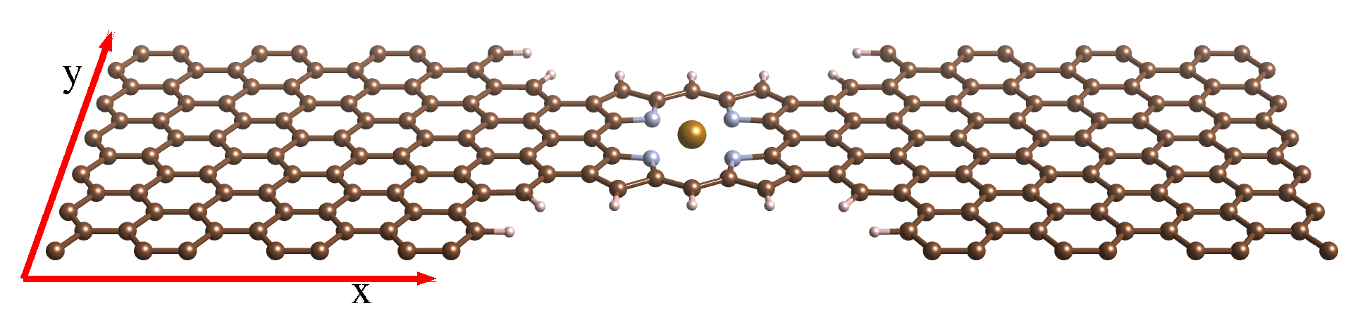
3. FeP Molecular Junction between Graphene Electrodes

The system under study consists of an iron-porphyrin molecule bonded to two semi-infinite graphene layers as shown in Figure 1. The graphene sheet extends continuously in the x y plane, and the dangling bonds of carbon atoms are saturated with hydrogens. The width of the nanojunction is three carbon-pair lines in the transverse direction, i.e., the smallest one in which the FeP molecule can be embedded. The lateral separation between periodically repeated porphyrins ensures that no interaction between them occurs. With this geometric arrangement we want to stress the 1-dimensional character of the junction, since the current is forced to flow through the FeP molecule.
In previous studies, FeP molecules are contacted with gold, which is the standard electrode material for metal-molecule junctions [12,13,14,15]. In all cases the molecule is bonded to the lead via a thiol anchor group, forcing the current to flow through a single atom. Besides this arrangement, also carbon-based electrodes such as graphene nanoribbons or carbon nanotubes have been proposed for contacting molecules [16,17,18,56,57], taking advantage of the low atomic mobility of graphene at room temperature, resulting in atomically stable electrodes [58]. In particular, the synthesis of an iron-porphyrin-like carbon nanotube has been reported, where a seamless incorporation of the FeP molecule in graphene results in excellent contacts between the active site and the conducting wires [59]. Given this background, we simulate a system in which the current is indeed forced to flow through the magnetic region and, at the same time, the 2D nature of graphene is fruitfully exploited in the contacts. In our junction the single bonding atom is replaced with a more extended contact with pure graphene leads.
Before performing geometric relaxation we determine the optimal size of the structure minimizing its total energy. The calculation is done considering only the central region and neglecting the outer 48 carbon atoms on each side, 24 belonging to the electrodes and 24 belonging to the buffer region where the perturbation effects induced in the scattering region should decay. The relaxation of the molecule contacted with graphene should indeed be influenced only by the first neighbors and not by the presence of additional external C atoms. The geometric optimization is performed considering the complete junction and relaxing all the atoms but the two electrodes plus an additional transverse line of C atoms. The embedding of an iron-porphyrin in a graphene junction has small effects on the structural properties of the molecule. The N–N distance in the direction parallel to the junction remains unchanged, while in the perpendicular direction the two N atoms approach by 0.03 Å. Consistently, Fe–N measures 1.98 Å to be compared with 1.99 Å in the isolated FeP.

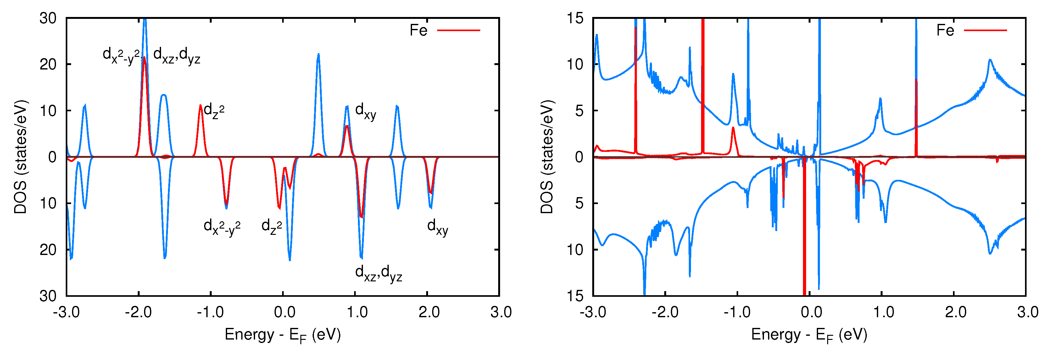
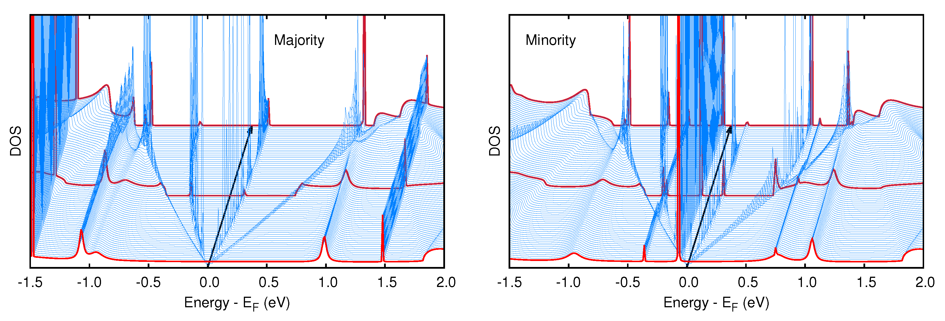
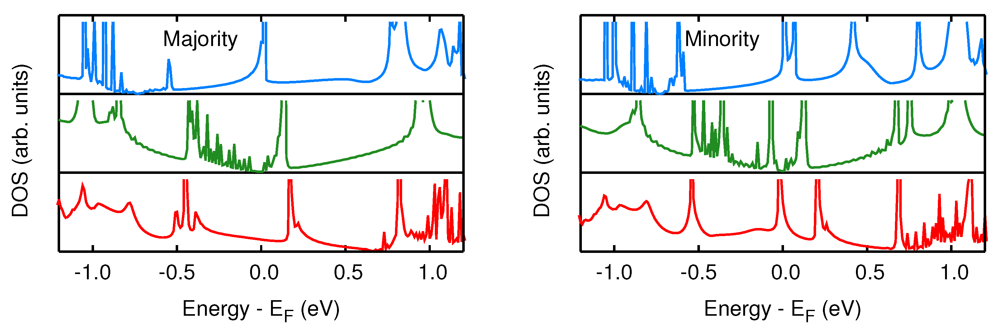
3.1. Spectral and Electronic Properties

The magnetic moment of the isolated FeP molecule measures 2.0 μ B and is localized on the Fe atom. In agreement with literature results [60] the occupancy of the 3d shell is ( d z 2 ) 2 ( d x 2 y 2 ) 2 ( d x z ) 1 ( d y z ) 1 (see Figure 2, left panel), the last two orbitals being degenerate as a consequence of the molecular symmetry.
The highest occupied molecular orbital (HOMO) of both spin components is a d z 2 Fe state. The spin-up and spin-down lowest unoccupied molecular orbitals (LUMO) have π character, and they are delocalized over the entire molecule, including minor contributions from Fe.
In the graphene-FeP nanojuction, the magnetic moment remains equal to 2.0 μ B . However, the longitudinal and transverse directions are no more equivalent, which implies the splitting of the d x z and d y z pair. This effect, together with a modification of the properties of FeP electronic states, induces a rearrangement of the orbital occupancy of FeP.
In the right panel of Figure 2 we report the total density of states of the nanojunction, along with its projection on the central Fe atom. The typical shape due to pristine graphene is clearly recognizable, along with several features related to the junction. The FeP fragment presents four occupied majority states and two minority ones. The former are the d z 2 and d x 2 y 2 orbitals, which display a localized character (sharp peaks at 2.4 eV and 1.44 eV), along with two d π states with strong hybridization between FeP and graphene. As concerns the minority component, only two sharp peaks d x 2 y 2 and d y z are visible below the Fermi level ( 0.34 and 0.05 eV, respectively). The unoccupied states are a localized d x y majority one and a more delocalized minority d y z overlaying to the sharp d z 2 . The non spin split state visible just above E F is in fact the unoccupied molecular orbital of lower energy. The slightly magnetic broad peaks situated at 1 eV are π molecular states hybridized with graphene.
The dispersion of different states can be analyzed considering the DOS for each k , as reported in Figure 3. The projected energy gap of the graphene electrodes is clearly visible in both spin components. As concerns the majority component, the hybridized states at 1.05 and 1.0 eV display a negligible dispersion. A similar behavior is found for the strictly localized state at ∼1.5 eV.
The dispersing state below the Fermi level and belonging to the projected gap is prevented to propagate into the bulk substrate, and displays a 1D character. In fact, in the region where the FeP molecule is connected with the electrodes the junction has a zig-zag edge of carbon atoms saturated with hydrogen, and these states are strictly localized [61,62,63]. The tiny dispersion shown by the molecular state just above E F indicates that the interaction between the molecule replicas along the y direction is negligible, and hence the transverse size of the junction is appropriately selected. In the minority component similar features can be pointed out, the main difference being an unoccupied edge state that enters in the gap in correspondence of the the mid-point of the Γ ¯ X ¯ path.

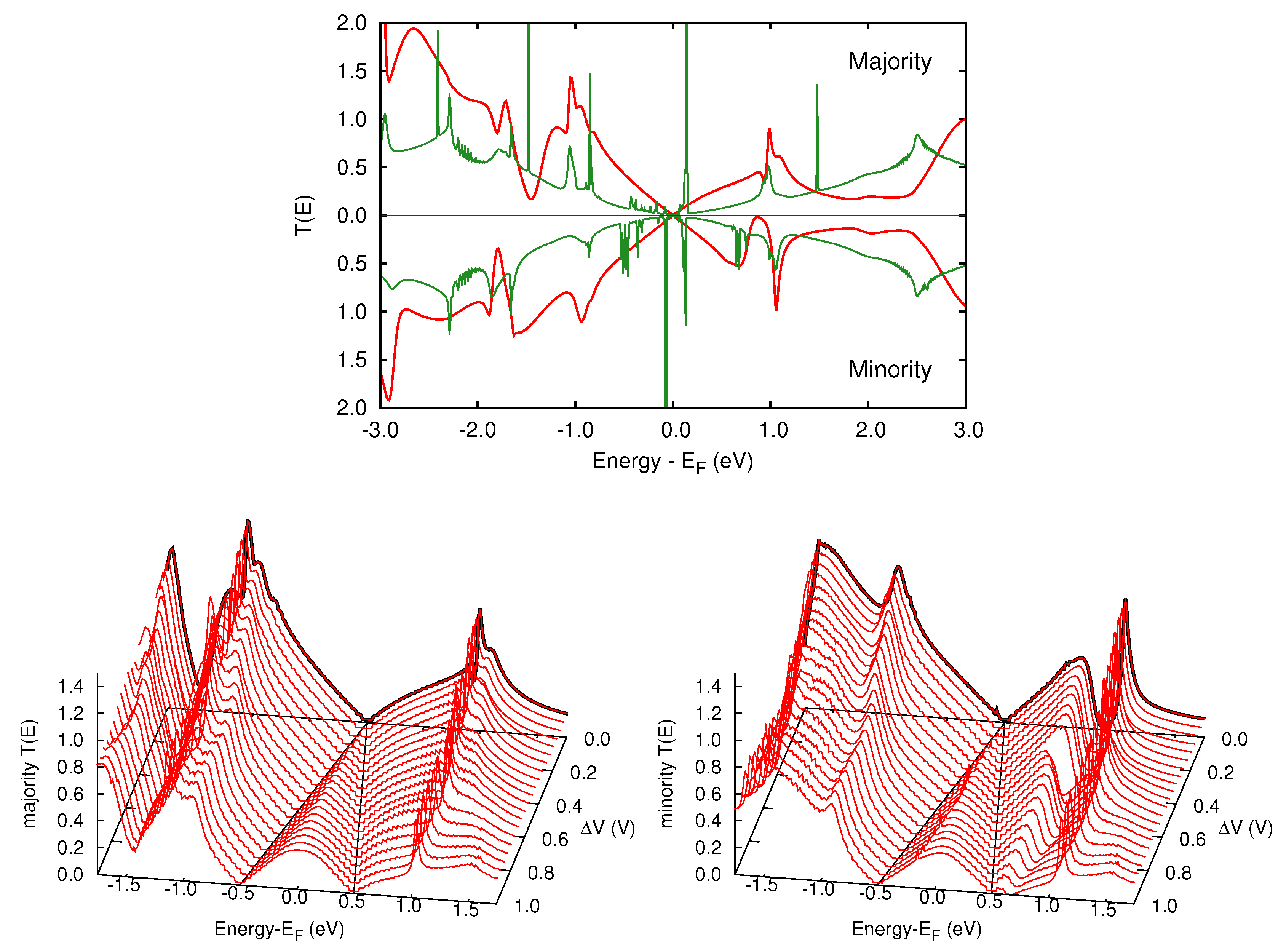
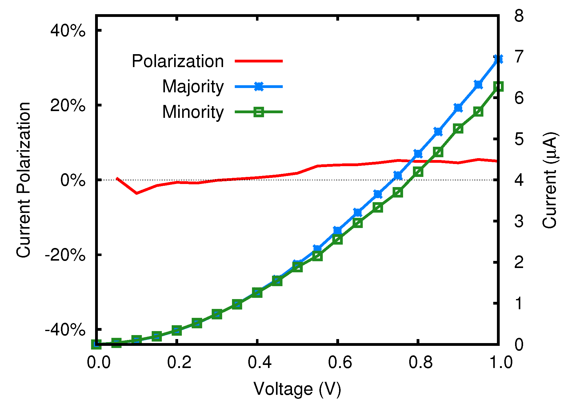
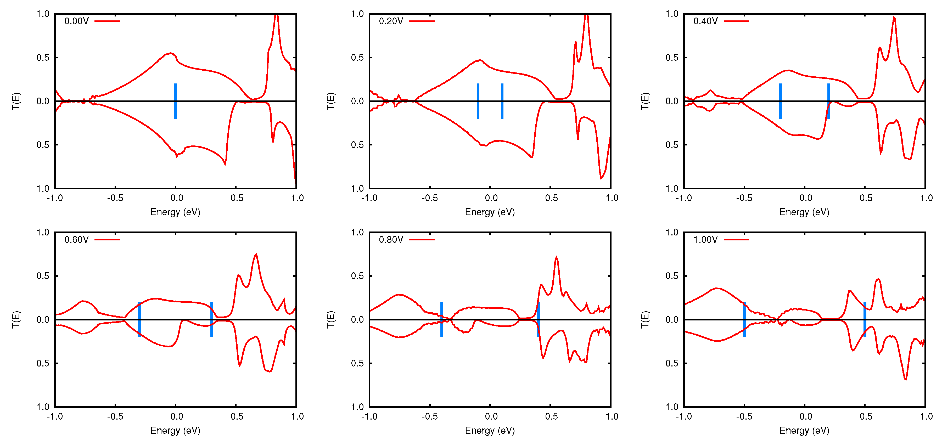
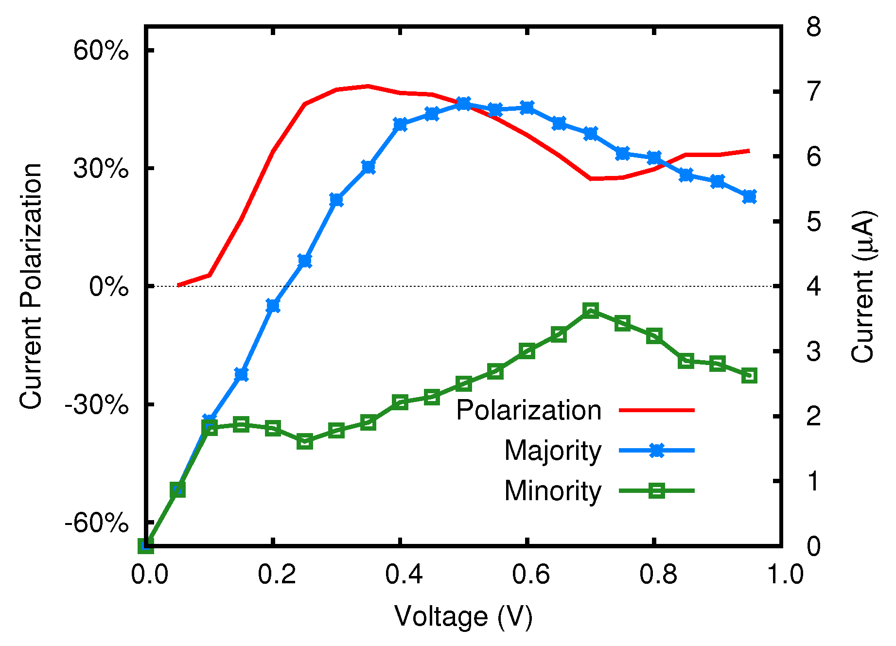
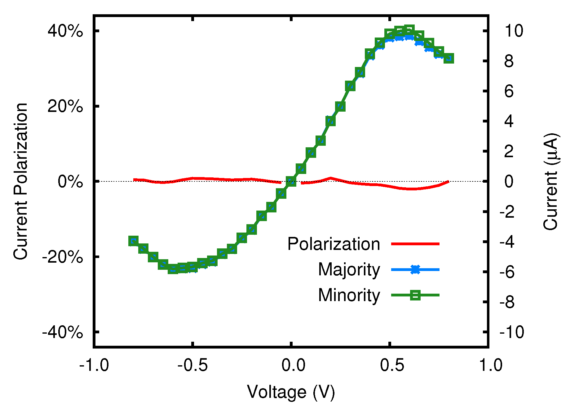
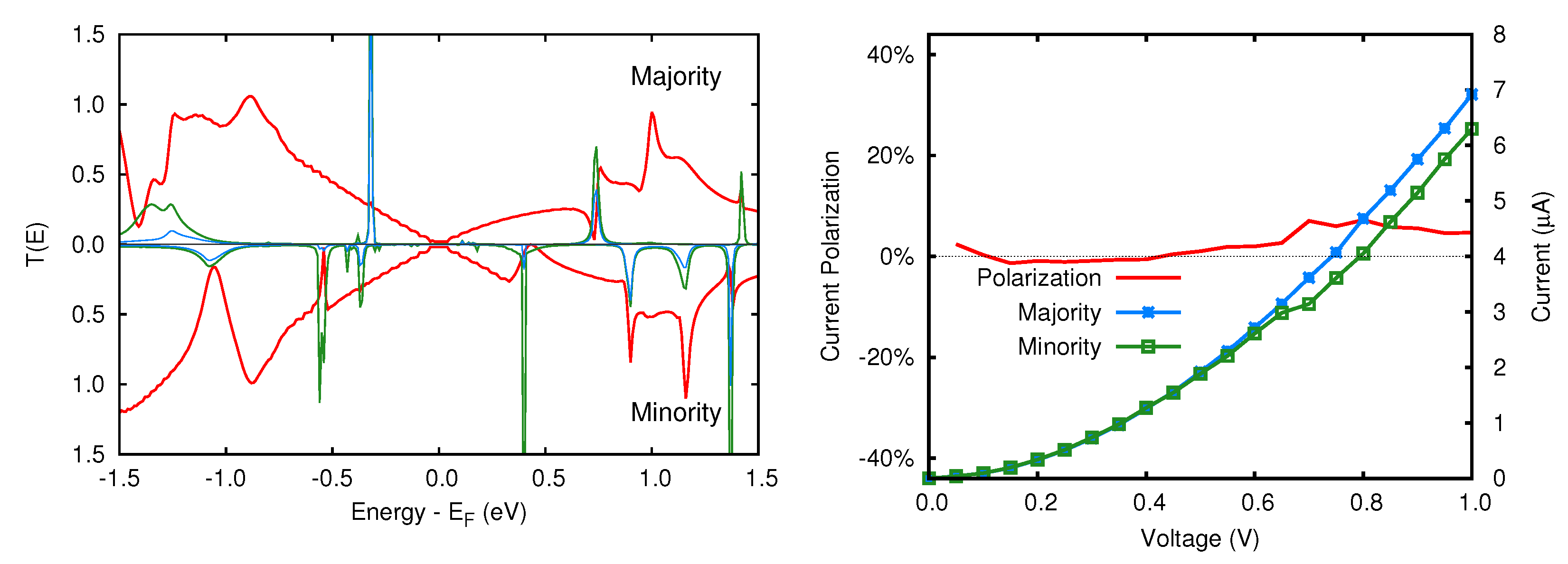
3.2. Transmission Properties

As extensively discussed in the case of transition metals adsorbed on graphene [64,65,66], the electronic states of iron produce different effects depending on their features. In this case study, since the two spin components of the FeP molecule are different, their hybridization with graphene induces an asymmetry (i.e., magnetism) also in its electronic structure and hence in its transport properties. The two spin components of the transmission function of the nanojunction with no applied bias are reported in the upper panel of Figure 4. In the same plot a green line represents the total density of states (DOS) of the nanojunction: several sharp peaks around the Fermi level are present, which can be attributed to the FeP moiety bridging the two semi-infinite graphene sheets. Due to the extremely localized nature of these states, the T ( E ) has a smooth shape, nicely reminding that of pristine graphene. Quite interestingly, this feature does not change even upon bias application Δ V , as can be seen in the lower panels of Figure 4.
Figure 5 shows the electronic current in the nanojunction, which is given by the following equation for each spin component:
I = e h d E f ( E , μ L ) f ( E , μ R ) T ( E ) ,
where μ L / R are the chemical potentials of the two electrodes and f the Fermi-Dirac distribution. At low biases the majority and minority spin components, I M a j and I M i n , are indistinguishable, and slightly differentiate only starting from 0.5 V. Accordingly, the spin polarization of the electronic current, defined as the percentage ratio ( I M a j I M i n ) / ( I M a j + I M i n ) [66], remains negligible along the entire bias range considered. We conclude that, despite the magnetic character of the junction, no relevant spin dependent behavior can be exploited in the bias range considered and the trends of the current at varying bias are almost graphene-like. A closer inspection of Figure 4 suggests however that a breakthrough in the design of a graphene-FeP based spintronic device is still possible. Indeed, though the electronic states localized onto the FeP moiety and close to the Fermi level have no relevant effect on the transmission function, this is not so for the FeP states at about 1.0 and 1.0 eV with respect to E F , and hence a strategy to build a spintronic device can be envisaged, as discussed in the next section.

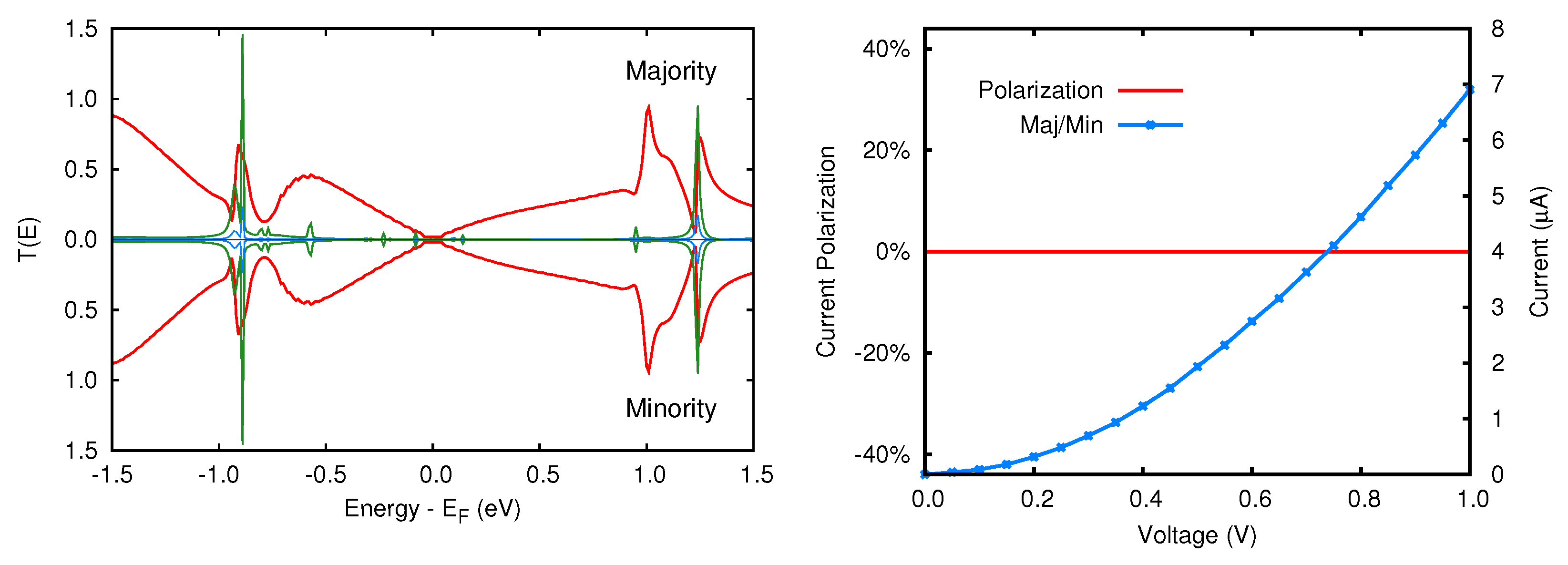
4. Effects of Doped Electrodes
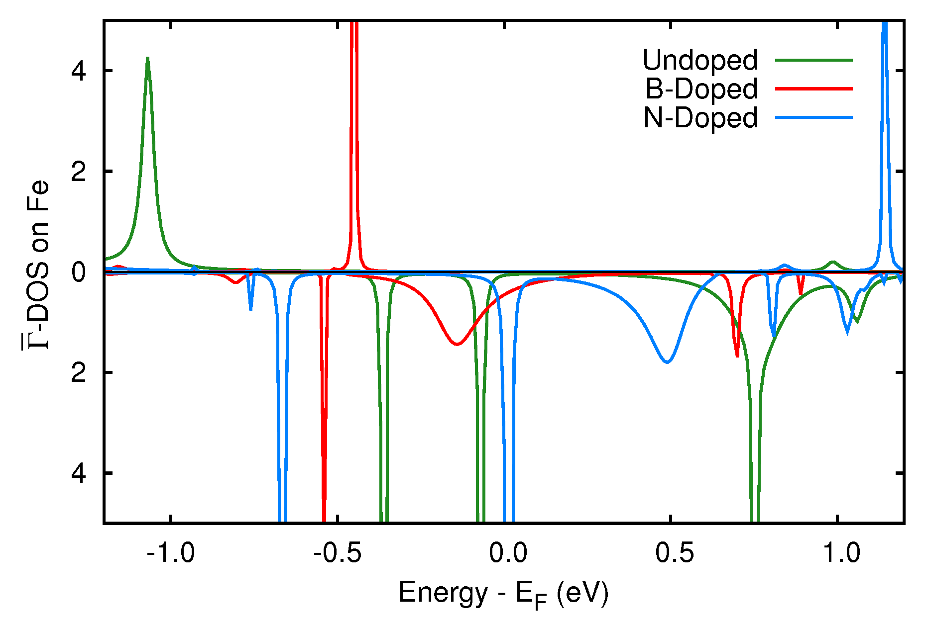
Chemical doping represents a natural way of increasing charge carriers density in graphene while preserving its remarkable transport properties [67,68]. Furthermore, doping of graphene with the elements adjacent to carbon in the periodic table, i.e., boron and nitrogen, has been experimentally demonstrated [67,69]. When dopants are introduced in the electrodes, the Fermi level is expected to shift with respect to the Dirac point, thus increasing significantly the DOS around E F . Remarkably, the shift of the Fermi level obtained by substituting C atoms with B or N is analogous to the common practice of applying a gate voltage to the device, thus controlling the nature and the concentration of charge carriers in transistors. Besides being interesting in itself, the case studies of B or N doped electrodes have therefore this more general valence. As for the system treated here, upon doping the states of FeP hybridized with graphene might get close to E F , producing remarkable effects on the transmission function of the device. The group III element boron introduces a hole in the electronic structure, i.e., it acts as a p-type dopant, while the group V element nitrogen donates an electron and thus acts as an n-type dopant. In the present investigation we simulated three different systems, obtained by introducing a quite diluted dopant concentration (∼2%, 1 substitutional atom on every 48 carbons) in both the left and the right electrodes. In the first case they are both doped with boron, in the second with nitrogen, and in the third one the left electrode contains boron atom and the right one contains nitrogen. Considering just the electrodes, doping does not alter the electronic structure in the proximity of the Dirac cone. However, substitution of carbon with boron induces a downshift of the Fermi level of about 0.75 eV, while the opposite is found in the case of nitrogen doping.
To understand whether the effects of the substitutional atoms on the electronic structure of the nanojunction are confined in the leads or involve the whole system, we calculated the spin-resolved DOS of the scattering regions, shown in Figure 6 together with the DOS of the undoped system. A careful inspection of the DOS reveals that the shift of the Fermi level of the electrodes induces an analogous effect in the whole system, and hence in the proximity of E F the DOS is no longer negligible.
The spin polarization of the current is related to the hybridization of the electronic states of Fe with the band structure of graphene close to the Fermi level. We therefore calculated the density of states projected on the Fe atoms in presence of dopants, to be compared with the case of pure electrodes (see Figure 7). In the majority component no states are visible in a wide energy region comprising the Fermi level, thus no differences with respect to the undoped system are expected. The single state at about 0.45 eV in the boron doped system is very sharp, does not hybridize with carbon and most likely has no influence on the transmission function. Differently, in the minority component many Fe states are present in the range from 1 to 1 eV. In particular, in the B-doped case a state at 0.2 eV displays a hybridized character, and a similar feature is visible in the N-doped system at 0.5 eV. The other peaks of Fe are very sharp and hence they are not expected to produce relevant effects on the transport properties. Overall, the electronic structure of the doped devices are very promising and worth of further investigation, as discussed in the next sections.

4.1. N-Doped System

When the graphene electrode is doped with a nitrogen atom the Fermi level is shifted 0.75 eV above the Dirac point (see Figure 6). The current flowing through the junction is shown in Figure 8. As the bias voltage increases, the current increases almost linearly up to about 0.4 V in the majority component, and up to 0.6 V in the minority case. At higher biases both components decrease, showing a marked Negative Differential Resistance (NDR) effect up to 0.8 V, where the trend is reversed. Overall, the spin polarization of the current does not reach appreciable values in the entire range considered. It is worth noting however that the polarization changes sign at about 0.6 V, where the majority spin current becomes greater than the minority component.
To investigate the causes of the NDR behavior we analyzed the transmission functions for different applied biases, as reported in Figure 9. At any voltage considered the transmission function of both spin components presents two vanishing regions. Those at energies below the Fermi level (∼−0.75 eV at 0.0 V bias) come from the shifting of the Dirac cone upon doping (see Figure 6). As the voltage increases, these gaps shift at higher energies, and eventually enter the bias window at voltages larger than 0.6 V, thus reducing the amplitude of T ( E ) and hence the current. Vanishing regions of T ( E ) at about 0.6 eV above the Fermi level are instead due to features peculiar of the nanojunction. As can be seen from Figure 9, already at 0.0 V the minority spin component presents a larger gap in the T ( E ) with respect to the majority one. Most likely, this is due to the electronic state of Fe strongly hybridized with the nanojunction (see Figure 7, broad blue peak at 0.5 eV). As the voltage increases these gaps in the T ( E ) shift at lower energies and, as can be seen in the 0.4 V panel of Figure 9, the dip in the minority spin component of the T ( E ) becomes structured and much larger than happens for the majority spin T ( E ) . These features provide a rationale for the NDR observed in the N-doped nanojunction, and for the steeper decrease of the minority spin current at high voltages with respect to the majority spin component. More importantly, they certify that to evaluate the transport properties of a system based on its electronic structure at zero voltage bias represents an unreliable approximation.

4.2. B-Doped System

In Figure 10 we report the current of the device with boron-doped electrodes. As observed in the case of N-doping, at very low biases the relation between I and V is linear, most likely due to the non vanishing DOS at the Fermi level. At ∼0.1 V the minority spin current reaches a plateau, while the majority spin current continues increasing. This effect is determined by a dip in the T ( E ) of the minority spin only, located at energies slightly lower than E F (see Figure 7, broad red peak at 0.2 eV). This feature is due to an electronic state partially localized on Fe and hybridized with the atoms of the nanojunction. The unbalance between majority and minority spin electronic states reflects in the spin polarization of the current, which reaches the remarkable value of about 50%.
At high voltages both spin components of the current decrease, and therefore also in the case of B-doped electrodes the nanojunction exhibits a range of negative differential resistance. This, in turn, is determined by the absence of electronic states at the Dirac point, upshifted by ∼0.75 eV with respect to the undoped system.

4.3. BN-Doped System

When the left and right electrodes are doped with boron and nitrogen, respectively, the system looses the left/right symmetry and hence the resulting current might exhibit different trends depending on the sign of the applied voltage. As can be seen in Figure 11, the current varies very regularly in both components at varying bias, and the relation between I and V is almost linear for small voltages. Starting from ± 0.5 V a NDR behavior is observed, most likely due to the inclusion in the bias window of the dips in the T ( E ) typical of the Dirac cone.
No spin polarization can be detected, which means that no electronic state partially localized on iron and hybridized with the remaining portion of the junction enters the bias window inducing a dip in the transmission function. The positive current, flowing from the B-doped electrode to the N-doped one, reaches a maximum value of about 10 μA at a voltage of 0.5 V. When the bias is reversed, the current measures just 6 μA, thus this system displays a partial rectification behavior.

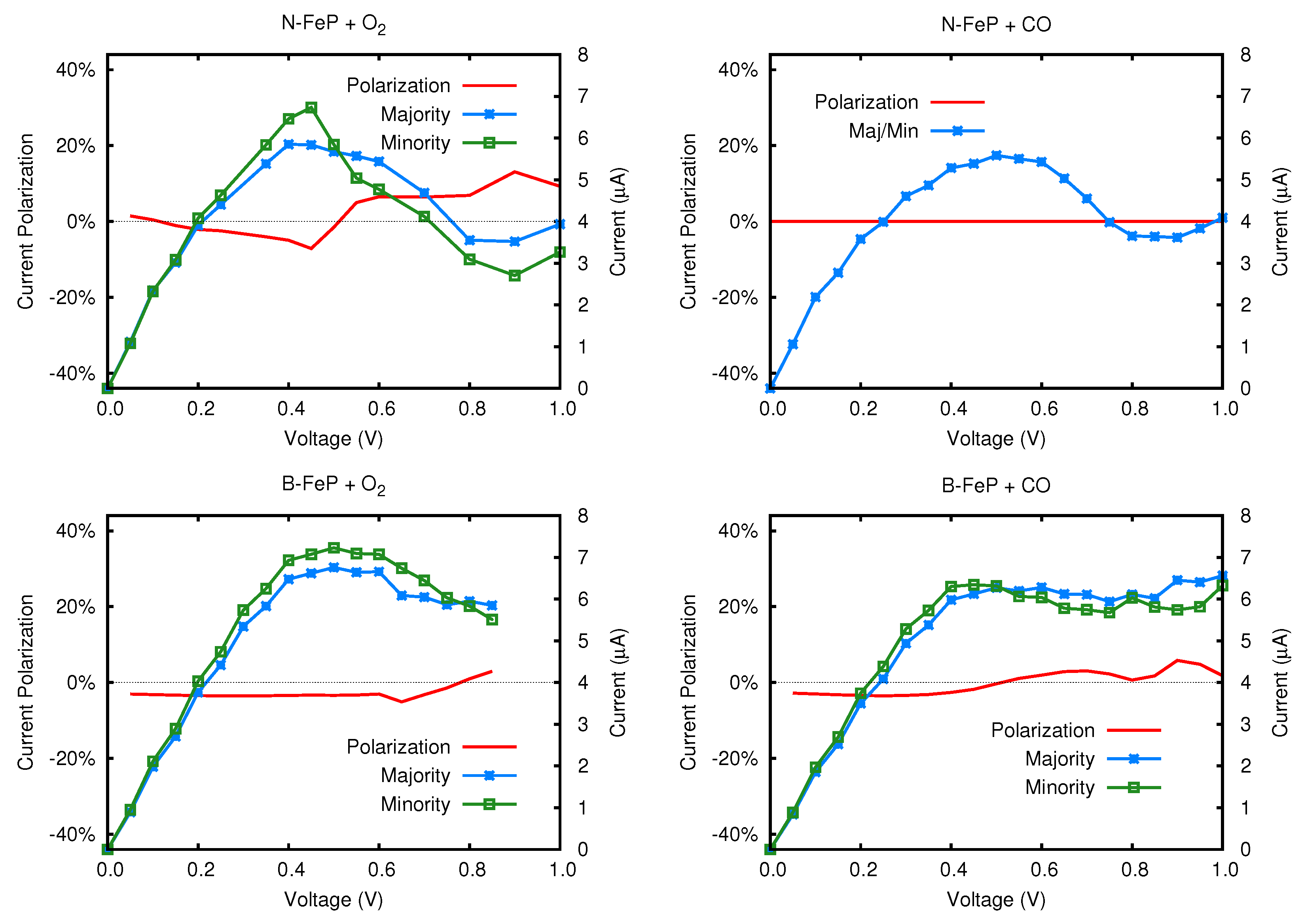
5. Gas Molecules Adsorption

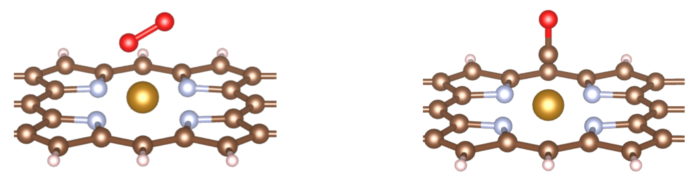
5.1. Geometric Structures

As can be seen in Figure 12, upon adsorption onto the junction the oxygen molecule connects to the Fe atom in an end-on geometry, driven by the interaction between Fe d z 2 and O2 π * orbitals. The –O2–FeP structure is bent with a Fe–O–O angle of about 107°. The O–O internuclear distance increases from 1.21 Å in the isolated gas phase molecule to 1.29 Å when adsorbed onto FeP. The adsorption energy is just 1.10 eV and, quite interestingly, the magnetic character of the junction is preserved. As concerns the carbonyl moiety, in the minimum energy configuration CO stands on top of the Fe atom, perpendicular to the graphene plane, with carbon pointing downwards. The C–O bond slightly elongates with respect to the free molecule, moving from 1.13 Å to 1.17 Å. The adsorption energy measures 2.00 eV, markedly larger than the value found for O2 and, at variance with this case, the electronic structure of the junction becomes non magnetic. These results compare well with available theoretical and experimental studies [70,71].

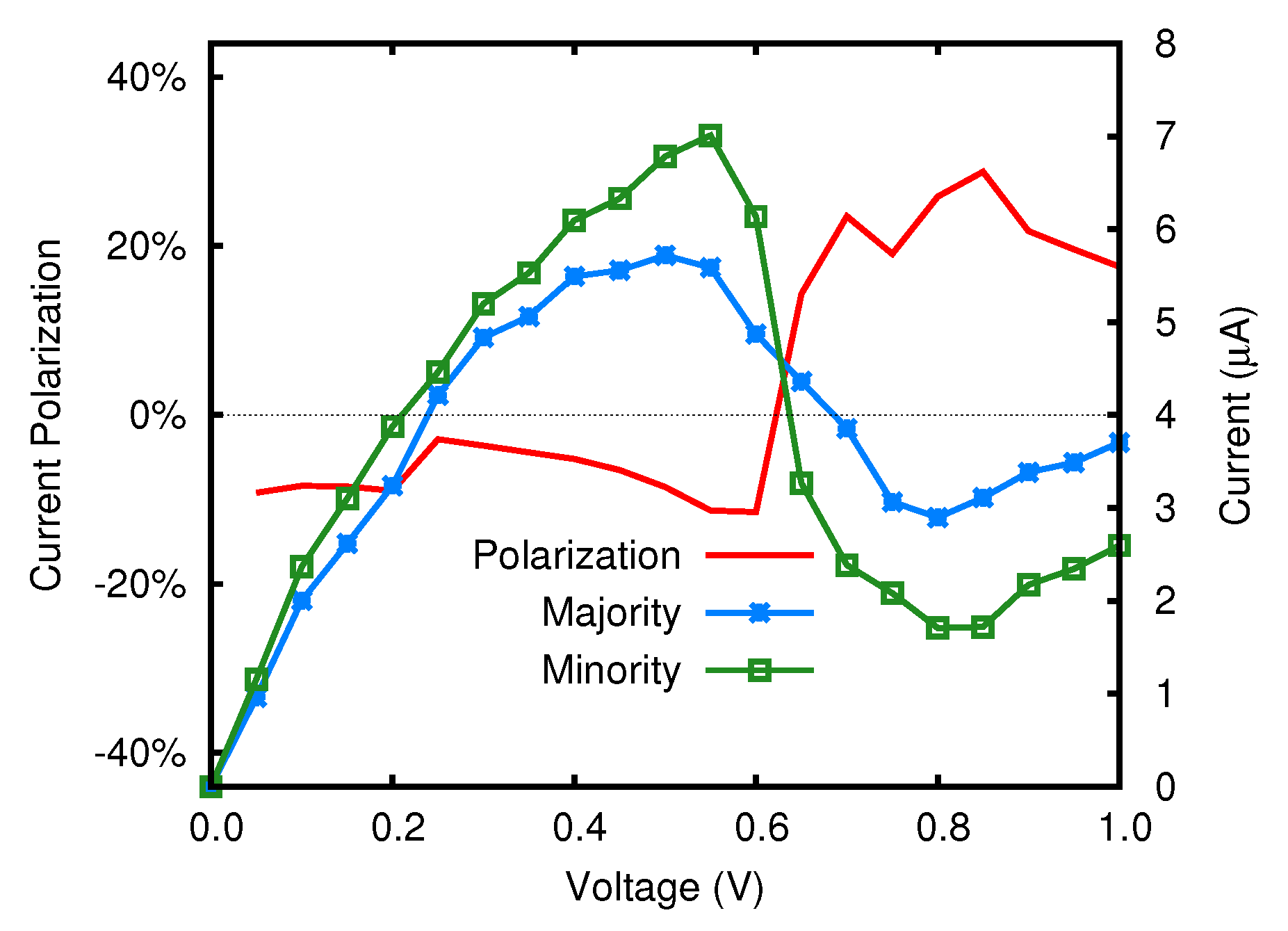
5.2. Transmission Function and Electronic Current

The transmission functions and the current of the FeP junction with an oxygen molecule adsorbed are reported in Figure 13. In detail, focusing on the majority spin component, the largely hybridized state around −1.3 eV causes a noticeable decrease in the T ( E ) , while the sharp peak at −0.3 eV does not influence the smooth trend of the transmission function in that energy region.
The two sharp states above the Fermi level give rise to Fano resonances [72,73]. As concerns the minority spin component, an analogous picture can be traced. A peculiar feature is due to the peak at ∼0.45 eV, which is responsible for a significant dip in the transmission function. The analysis of the electronic current indicates that for low biases the two spin components are indistinguishable, but at 0.7 V the minority component increases less steeply than the majority one, due to the inclusion in the bias window of the minority electronic state above mentioned. Overall, the current has the smooth trend typical of pristine graphene as already observed in the FeP nanojunction (see Figure 5), where the spin polarization is indeed minimal. In conclusion, the role played by oxygen interaction with iron is negligible, despite a sizable hybridization of its electronic states with the ones of Fe.
The features described for the O2-adsorbed junction apply also in the case of the CO molecule, and even more so, as can be observed in Figure 14. First, the system becomes non magnetic. Second, the mixed Fe/CO electronic states that perturb the transmission function fall at −0.9 and +1.25 eV, i.e., out of the bias window considered in this study. As a result, the two spin components of the current are identical, and closely match the trend already discussed for the majority spin component in the pristine nanojunction.
In Figure 15 we reported the spin-polarized current for the nanojunction with O2 or CO adsorbed molecules, when contacted with N- or B-doped electrodes. As can be seen by comparing the upper panels of the figure with Figure 8, no relevant effect due to adsorption of gas molecules can be devised when N-doped electrodes are considered. The main trends of both spin components of the current are preserved, including the NDR effect starting at about 0.5 V. The carbonyl moiety is indeed able to quench magnetism in the junction, thus annihilating the spin polarization of the current. However, its values are very small even in the pristine junction, thus preventing any practical application of such system. A comparison between bottom panels in Figure 15 and Figure 10 reveals that quite interesting effects might be detected when p-doped electrodes are considered. Indeed, either upon adsorption of O2 and CO the minority spin component of the current is largely enhanced, and it becomes very similar to the majority spin component. This means that spin polarization of the current, which in the pristine junction ranges from 25% to 50%, is almost completely quenched upon molecules adsorption, thus disclosing the possibility to build up spintronic nanosensors based on a graphene-FeP junction.

6. Conclusions

We investigated an iron-porphyrin junction contacted to graphene leads and we characterized its electron transport properties to verify its potential applications as a gas sensor device. We tackled the complex topic of electron transport with particular attention to the spin dependent properties. We dealt with open, non periodic systems whose electronic structure cannot be easily obtained with standard methods. For the calculation of the charge transport we adopted non-equilibrium Green’s Function formalism, which provides a rigorous description of the ballistic quantum transport and enables self-consistent calculations of the charge density under a finite bias voltage, a fundamental requirement to obtain reliable results [74].
When the magnetic junction contacts pristine graphene electrodes, no significant effects can be pointed out. However, our study clearly highlights the role played by the hybridization between the electronic states of Fe and the propagating graphene ones on the electron transmission function of the junction. When the electrodes are doped with boron atoms a relevant current polarization is observed. The doping of electrodes with nitrogen atoms gives instead rise to an interesting effect, namely the Negative Differential Resistance, consisting in a reduction of the current at increasing voltages.
Finally, we addressed the problem of the possible exploitation of this molecular junction in a gas sensor device. We investigated the changes in the charge transport properties upon adsorption of gas molecules, O2 and CO, and demonstrated that they induce quite small effects on the current. However, an almost complete quenching of the spin-polarized current is observed when B-doped electrons are considered, which is a challenging topic for future advances in the field.

Author Contributions

Conceptualization, E.d.C. and M.I.T.; Formal analysis, E.d.C. and R.S.; Investigation, E.d.C., Fausto Cargnoni and M.I.T.; Methodology, E.d.C.; Supervision, M.I.T.; Writing—original draft, E.d.C.; Writing—review and editing, F.C. and R.S. All authors have read and agreed to the published version of the manuscript.

Funding

This research received no external funding.

Acknowledgments

Several discussions with Davide Ceresoli are acknowledged.

Conflicts of Interest

The authors declare no conflict of interest.

References and Note

  1. Aviram, A.; Ratner, M.A. Molecular rectifiers. Chem. Phys. Lett. 1974, 29, 277. [Google Scholar] [CrossRef]
  2. Tao, N.J. Probing Potential-Tuned Resonant Tunneling through Redox Molecules with Scanning Tunneling Microscopy. Phys. Rev. Lett. 1996, 76, 4066. [Google Scholar] [CrossRef] [PubMed]
  3. Green, J.E.; Choi, J.W.; Boukai, A.; Bunimovich, Y.; Johnston-Halperin, E.; DeIonno, E.; Luo, Y.; Sheriff, B.A.; Xu, K.; Shin, Y.S.; et al. A 160-kilobit molecular electronic memory patterned at 1011 bits per square centimetre. Nature 2007, 445, 414. [Google Scholar] [CrossRef] [PubMed]
  4. Benesch, C.; Rode, M.F.; Čížek, M.; Härtle, R.; Rubio-Pons, O.; Thoss, M.; Sobolewski, A.L. Switching the Conductance of a Single Molecule by Photoinduced Hydrogen Transfer. J. Phys. Chem. C 2009, 113, 10315. [Google Scholar] [CrossRef]
  5. Li, Y.; Yang, C.; Guo, X. Single-Molecule Electrical Detection: A Promising Route toward the Fundamental Limits of Chemistry and Life Science. Acc. Chem. Res. 2020, 53, 159. [Google Scholar] [CrossRef] [PubMed]
  6. Rocha, A.R.; Garcia-Suarez, V.M.; Bailey, S.W.; Lambert, C.J.; Ferrer, J.; Sanvito, S. Towards molecular spintronics. Nat. Mater. 2005, 5, 335. [Google Scholar] [CrossRef]
  7. Liu, X.; Wang, T.; Niu, L.; Wang, Y.; Zhang, Q. Magnetic proximity, magnetoresistance and spin filtering effect in a binuclear ferric phthalocyanine from first principles. J. Phys. D Appl. Phys. 2020, 53, 035305. [Google Scholar] [CrossRef]
  8. Sanvito, S. Spintronics goes plastic. Nat. Mater. 2007, 6, 803. [Google Scholar] [CrossRef]
  9. Szulczewski, G.; Sanvito, S.; Coey, M. A spin of their own. Nat. Mater. 2009, 8, 693. [Google Scholar] [CrossRef]
  10. Sanvito, S. Molecular spintronics. Chem. Soc. Rev. 2011, 40, 3336. [Google Scholar] [CrossRef]
  11. Lee, S.U.; Belosludov, R.V.; Mizuseki, H.; Kawazoe, Y. The Role of Aromaticity and the π-Conjugated Framework in Multiporphyrinic Systems as Single-Molecule Switches. Small 2008, 7, 962. [Google Scholar] [CrossRef] [PubMed]
  12. Wang, N.; Liu, H.; Zhao, J.; Cui, Y.; Xu, Z.; Ye, Y.; Kiguchi, M.; Murakoshi, K. Theoretical investigation on the electron transport path through the Porphyrin molecules and chemisorption of CO. J. Phys. Chem. C 2009, 113, 7416. [Google Scholar] [CrossRef]
  13. Li, Y.W.; Yao, J.H.; Liu, C.J.; Yang, J.W.; Yang, C.L. Theoretical investigation of the O2 adsorption effect in the electron transport of single Fe-porphyrin molecule. Phys. Lett. A 2009, 373, 3974. [Google Scholar] [CrossRef]
  14. Kondo, H.; Nara, J.; Ohno, T. Possibility of gas sensor using electronic transport properties of iron-porphyrin molecular junction system. J. Phys. Chem. C 2011, 115, 6886. [Google Scholar] [CrossRef]
  15. Toyoda, K. Theoretical investigation of chemical spin doping into single porphyrin junctions toward ultrahigh-sensitive nitric oxide sensor. Jpn. J. Appl. Phys. 2012, 51, 045202. [Google Scholar] [CrossRef]
  16. Huang, J.; Wang, W.; Yang, S.; Su, H.; Li, Q.; Yang, J. A theoretical study of spin-polarized transport properties of planar four-coordinate Fe complexes. Chem. Phys. Lett. 2012, 539, 102. [Google Scholar] [CrossRef]
  17. Huang, J.; Xu, K.; Lei, S.; Su, H.; Yang, S.; Li, Q.; Yang, J. Iron-phthalocyanine molecular junction with high spin filter efficiency and negative differential resistance. J. Chem. Phys. 2012, 136, 064707. [Google Scholar] [CrossRef]
  18. Huang, J.; Wang, W.; Yang, S.; Li, Q.; Yang, J. Efficient spin filter based on FeN4 complexes between carbon nanotube electrodes. Nanotechnology 2012, 23, 255202. [Google Scholar] [CrossRef]
  19. Lörtscher, E. Wiring molecules into circuits. Nat. Nanotech. 2013, 8, 381. [Google Scholar] [CrossRef]
  20. Bruot, C.; Hihath, J.; Tao, N. Mechanically controlled molecular orbital alignment in single molecule junctions. Nat. Nanotech. 2011, 7, 35. [Google Scholar] [CrossRef]
  21. Liang, W.; Shores, M.O.; Bockrath, M.; Long, J.R.; Park, H. Kondo resonance in a single-molecule transistor. Nature 2002, 417, 725. [Google Scholar] [CrossRef] [PubMed]
  22. Guédon, C.M.; Valkenier, H.; Markussen, T.; Thygesen, K.S.; Hummelen, J.C.; van der Molen, S.J. Observation of quantum interference in molecular charge transport. Nat. Nanotech. 2012, 7, 305. [Google Scholar] [CrossRef] [PubMed] [Green Version]
  23. Metzger, R.M.; Chen, B.; Höpfner, U.; Lakshmikantham, M.V.; Vuillaume, D.; Kawai, T.; Wu, X.; Tachibana, H.; Hughes, T.V.; Sakurai, H.; et al. Unimolecular Electrical Rectification in Hexadecylquinolinium Tricyanoquinodimethanide. J. Am. Chem. Soc. 1997, 119, 10455. [Google Scholar] [CrossRef]
  24. Kubatkin, S.; Danilov, A.; Hjort, M.; Cornil, J.; Brédas, J.L.; Stuhr-Hansen, N.; Hedegard, P.; Bjornholm, T. Single-electron transistor of a single organic molecule with access to several redox states. Nature 2003, 425, 698. [Google Scholar] [CrossRef] [PubMed]
  25. Quek, S.Y.; Kamenetska, M.; Steigerwald, M.L.; Choi, H.J.; Louie, S.G.; Hybertsen, M.S.; Neaton, J.B.; Venkataraman, L. Mechanically-Controlled Binary Conductance Switching of a Single-Molecule Junction. Nat. Nanotech. 2009, 4, 230. [Google Scholar] [CrossRef] [PubMed] [Green Version]
  26. Thiele, S.; Balestro, F.; Ballou, R.; Klyatskaya, S.; Ruben, M.; Wernsdorfer, W. Electrically driven nuclear spin resonance in single-molecule magnets. Science 2014, 344, 1135. [Google Scholar] [CrossRef]
  27. Nazin, G.V.; Qiu, X.H.; Ho, W. Visualization and Spectroscopy of a Metal-Molecule-Metal Bridge. Science 2003, 302, 77. [Google Scholar] [CrossRef]
  28. He, Y.; Garnica, M.; Bischoff, F.; Ducke, J.; Bocquet, M.L.; Batzill, M.; Auwärter, W.; Barth, J.V. Fusing tetrapyrroles to graphene edges by surface-assisted covalent coupling. Nat. Chem. 2017, 9, 33. [Google Scholar] [CrossRef]
  29. Zeng, J.; Chen, K.Q. A nearly perfect spin filter and a spin logic gate based on a porphyrin/graphene hybrid material. Phys. Chem. Chem. Phys. 2018, 20, 3997. [Google Scholar] [CrossRef]
  30. Dayen, J.F.; Ray, S.J.; Karis, O.; Vera-Marun, I.J.; Kamalakar, M.V. Two-dimensional van der Waals spinterfaces and magnetic-interfaces. App. Phys. Rev. 2020, 7, 011303. [Google Scholar] [CrossRef] [Green Version]
  31. Han, W.; Kawakami, R.K.; Gmitra, M.; Fabian, J. Graphene spintronics. Nat. Nanotech. 2014, 9, 794. [Google Scholar] [CrossRef] [PubMed]
  32. Huang, J.; Wan, Q. Gas Sensors Based on Semiconducting Metal Oxide One-Dimensional Nanostructures. Sensors 2009, 9, 9903. [Google Scholar] [CrossRef] [PubMed]
  33. Kim, H.W.; Kwon, Y.J.; Mirzaei, A.; Kang, S.Y.; Choi, M.S.; Bang, J.H.; Kim, S.S. Synthesis of zinc oxide semiconductors-graphene nanocomposites by microwave irradiation for application to gas sensors. Sensor Actuators B Chem. 2017, 249, 590–601. [Google Scholar] [CrossRef]
  34. Chen, H.; Bo, R.; Shrestha, A.; Xin, B.; Nasiri, N.; Zhou, J.; Di Bernardo, I.; Dodd, A.; Saunders, M.; Lipton-Duffin, J.; et al. NiO–ZnO Nanoheterojunction Networks for Room-Temperature Volatile Organic Compounds Sensing. Adv. Opt. Mater. 2018, 6, 1800677. [Google Scholar] [CrossRef]
  35. Yang, J.; Liu, J.; Xu, Y.; Li, X.; Wu, J.; Han, Y.; Wang, Z.; Zhang, X. Enhanced selective acetone-sensing performance of hierarchical hollow SnO2/a-Fe2O3 microcubes. J. Mater. Chem. C 2019, 7, 11984. [Google Scholar] [CrossRef]
  36. Hittini, W.; Abu-Hani, A.F.; Reddy, N.; Mahmoud, S.T. Cellulose-copper oxide hybrid nanocomposites membranes for H2S gas detection at low temperatures. Sci. Rep. 2020, 10, 2940. [Google Scholar] [CrossRef] [Green Version]
  37. Park, J.; Pasupathy, A.N.; Goldsmith, J.I.; Chang, C.; Yaish, Y.; Petta, J.R.; Rinkoski, M.; Sethna, J.P.; Abruña, H.D.; McEuen, P.L.; et al. Coulomb blockade and the Kondo effect in single-atom transistors. Nature 2002, 417, 722. [Google Scholar] [CrossRef]
  38. Chen, Y.; Prociuk, A.; Perrine, T.; Dunietz, B.D. Spin-dependent electronic transport through a porphyrin ring ligating an FeII atom: An ab initio study. Phys. Rev. B 2006, 74, 245320. [Google Scholar] [CrossRef]
  39. Okuno, Y.; Yokoyama, S. Theoretical study of molecular rectification in porphyrin dimer. Thin Solid Films 2008, 516, 2630. [Google Scholar] [CrossRef]
  40. Salazar-Salinas, K.; Jauregui, L.A.; Kubli-Garfias, C.; Seminario, J.M. Molecular biosensor based on a coordinated iron complex. J. Chem. Phys. 2009, 130, 105101. [Google Scholar] [CrossRef] [PubMed]
  41. Perdew, J.P.; Burke, K.; Ernzerhof, M. Generalized gradient approximation made simple. Phys. Rev. Lett. 1996, 77, 3865. [Google Scholar] [CrossRef] [PubMed] [Green Version]
  42. Troullier, N.; Martins, J.L. Efficient pseudopotentials for plane-wave calculations. Phys. Rev. B 1991, 43, 1993. [Google Scholar] [CrossRef] [PubMed]
  43. Soler, J.M.; Artacho, E.; Gale, J.D.; García, A.; Junquera, J.; Ordejón, P.; Sánchez-Portal, D. The SIESTA method for ab initio order-N materials simulations. J. Phys. Condens. Matter 2002, 14, 2745. [Google Scholar] [CrossRef] [Green Version]
  44. Landauer, R. Spatial Variation of Currents and Fields Due to Localized Scatterers in Metallic Conduction. IBM J. Res. Dev. 1957, 1, 233. [Google Scholar] [CrossRef]
  45. Landauer, R. Electrical resistance of disordered one-dimensional lattices. Phil. Mag. 1970, 21, 863. [Google Scholar] [CrossRef]
  46. Boumrar, H.; Hamidi, M.; Zenia, H.; Lounis, S. Equivalence of wave function matching and Green’s functions methods for quantum transport: Generalized Fisher-Lee relation. J. Phys. Cond. Matter 2020. [Google Scholar] [CrossRef] [Green Version]
  47. Keldysh, L.V. Diagram technique for nonequilibrium processes. Sov. Phys. JETP 1965, 20, 1018. [Google Scholar]
  48. Caroli, C.; Combescot, R.; Nozieres, P.P.; Saint-James, D. Direct calculation of the tunneling current. J. Phys. C Solid State Phys. 1971, 4, 916. [Google Scholar] [CrossRef]
  49. Brandbyge, M.; Mozos, J.L.; Ordejón, P.; Taylor, J.; Stokbro, K. Density-Functional Method for Nonequilibrium Electron Transport. Phys. Rev. B 2002, 65, 165401. [Google Scholar] [CrossRef] [Green Version]
  50. Papior, N.; Lorente, N.; Frederiksen, T.; García, A.; Brandbyge, M. Improvements on non-equilibrium and transport Green function techniques: The next-generation transiesta. Comput. Phys. Commun. 2017, 212, 8. [Google Scholar] [CrossRef] [Green Version]
  51. Fisher, D.S.; Lee, P.A. Relation between conductivity and transmission matrix. Phys. Rev. B 1981, 23, 6851. [Google Scholar] [CrossRef] [Green Version]
  52. Sanvito, S.; Lambert, C.J.; Jefferson, J.H.; Bratkovsky, A.M. General Green’s-function formalism for transport calculations with spd Hamiltonians and giant magnetoresistance in Co- and Ni-based magnetic multilayers. Phys. Rev. B 1999, 59, 11936. [Google Scholar] [CrossRef] [Green Version]
  53. Levy Yeyati, A.; Buttiker, M. Scattering phases in quantum dots: An analysis based on lattice models. Phys. Rev. B 2000, 62, 7307. [Google Scholar] [CrossRef] [Green Version]
  54. Paulsson, M. Non Equilibrium Green’s Functions for Dummies: Introduction to the One Particle NEGF equations. arXiv 2008, arXiv:cond-mat/0210519. [Google Scholar]
  55. For the calculation of the non-equilibrium Green’s function we used an integration path in the complex-energy plane constituted by 38 points for the Gaussian quadrature, 32 energy point near the real axis (m(E) = 10−5 eV) in the bias windows and 16 poles on the imaginary axis of the energy. To work-out the values of the electron current we used a finer k-point mesh equal to 50 points in the 1D Brillouin zone.
  56. Guo, X.; Small, J.P.; Klare, J.E.; Wang, Y.; Purewal, M.S.; Tam, I.M.; Hong, B.H.; Caldwell, R.; Huang, L.; O’Brien, S.; et al. Covalently Bridging Gaps in Single-Walled Carbon Nanotubes with Conducting Molecules. Science 2006, 311, 356. [Google Scholar] [CrossRef] [PubMed] [Green Version]
  57. Marquardt, C.W.; Grunder, S.; Baszczyk, A.; Dehm, S.; Hennrich, F.; von Löhneysen, H.; Mayor, M.; Krupke, R. Electroluminescence from a single nanotube-molecule-nanotube junction. Nat. Nanotech. 2010, 5, 863. [Google Scholar] [CrossRef]
  58. Prins, F.; Barreiro, A.; Ruitenberg, J.W.; Seldenthuis, J.S.; Aliaga-Alcalde, N.; Vandersypen, L.M.K.; van der Zant, H.S.J. Room-Temperature Gating of Molecular Junctions Using Few-Layer Graphene Nanogap Electrodes. Nano Lett. 2011, 11, 4607. [Google Scholar] [CrossRef] [Green Version]
  59. Lee, D.H.; Lee, W.J.; Lee, W.J.; Kim, S.O.; Kim, Y.H. Theory, synthesis and oxygen reduction catalysis of Fe-porphyrin-like carbon nanotube. Phys. Rev. Lett. 2011, 106, 175502. [Google Scholar] [CrossRef]
  60. Liao, M.S.; Watts, J.D.; Huang, M.J. FeII in Different Macrocycles: Electronic Structures and Properties. J. Phys. Chem. A 2005, 109, 7988. [Google Scholar] [CrossRef]
  61. Wassmann, T.; Seitsonen, A.P.; Saitta, A.M.; Lazzeri, M.; Mauri, F. Structure, Stability, Edge States, and Aromaticity of Graphene Ribbons. Phys. Rev. Lett. 2008, 101, 096402. [Google Scholar] [CrossRef] [Green Version]
  62. Ijäs, M.; Ervasti, M.; Uppstu, A.; Liljeroth, P.; van der Lit, J.; Swart, I.; Harju, A. Electronic states in finite graphene nanoribbons: Effect of charging and defects. Phys. Rev. B 2013, 88, 075429. [Google Scholar] [CrossRef] [Green Version]
  63. Yamanaka, A.; Okada, S. Energetics and electronic structure of graphene nanoribbons under a lateral electric field. Carbon 2016, 96, 351. [Google Scholar] [CrossRef] [Green Version]
  64. del Castillo, E.; Cargnoni, F.; Achilli, S.; Tantardini, G.; Trioni, M.I. Spin asymmetric band gap opening in graphene by Fe adsorption. Surf. Sci. 2015, 634, 62–67. [Google Scholar] [CrossRef]
  65. del Castillo, E.; Cargnoni, F.; Soave, R.; Trioni, M.I. Spin-polarized charge transfer induced by transition metal adsorption on graphene. Phys. Scripta 2016, 91, 1–7. [Google Scholar] [CrossRef]
  66. del Castillo, E.; Achilli, S.; Cargnoni, F.; Ceresoli, D.; Soave, R.; Trioni, M.I. Spin-filtering in graphene junctions with Ti and Co adsorbates. Chem. Phys. 2016, 478, 91–96. [Google Scholar] [CrossRef]
  67. Panchakarla, L.S.; Subrahmanyam, K.S.; Saha, S.K.; Govindaraj, A.; Krishnamurthy, H.R.; Waghmare, U.V.; Rao, C.N.R. Synthesis, Structure, and Properties of Boron- and Nitrogen-Doped Graphene. Adv. Mater. 2009, 21, 4726. [Google Scholar] [CrossRef]
  68. Lherbier, A.; Blase, X.; Niquet, Y.M.; Triozon, F.; Roche, S. Charge Transport in Chemically Doped 2D Graphene. Phys. Rev. Lett. 2008, 101, 036808. [Google Scholar] [CrossRef] [Green Version]
  69. Lin, Y.C.; Lin, C.Y.; Chiu, P.W. Controllable graphene N-doping with ammonia plasma. Appl. Phys. Lett. 2010, 96, 133110. [Google Scholar] [CrossRef]
  70. Rovira, C.; Ballone, P.; Parrinello, M. A density functional study of iron-porphyrin complexes. Chem. Phys. Lett. 1997, 271, 247. [Google Scholar] [CrossRef]
  71. Momenteau, M.; Reed, C.A. Synthetic Heme Dioxygen Complexes. Chem. Rev. 1994, 94, 659. [Google Scholar] [CrossRef]
  72. Fano, U. Effects of Configuration Interaction on Intensities and Phase Shifts. Phys. Rev. 1961, 124, 1866–1878. [Google Scholar] [CrossRef]
  73. Nöckel, J.U.; Stone, A.D. Resonance line shapes in quasi-one-dimensional scattering. Phys. Rev. B 1994, 50, 17415–17432. [Google Scholar] [CrossRef] [PubMed] [Green Version]
  74. Datta, S. Electronic Transport in Mesoscopic Systems; Cambridge University Press: Cambridge, UK, 1995. [Google Scholar]
Figure 1. Fe porphyrin molecule contacted to graphene electrodes.
Magnetochemistry 06 00027 g001
Figure 2. Left panel: Spin-resolved energy levels of the isolated FeP molecule. The red lines represent the contribution of Fe to the molecular orbitals of the porphyrin. Right panel: Spin-resolved total density of states (DOS) of the FeP junction (blue line), along with its projection on the atomic orbitals of Fe (red line).
Magnetochemistry 06 00027 g002
Figure 3. k -resolved DOS for the two spin components. The red lines at Γ ¯ , X ¯ and at the mid-point of the Γ ¯ X ¯ path are highlighted for a better reading of the plot ( Γ ¯ being in the foreground and X ¯ in the background). The black arrow represents the Fermi level.
Magnetochemistry 06 00027 g003
Figure 4. Upper panel: T ( E ) at zero bias of the nanojunction (red line), along with the total DOS (green line). Lower panels: transmission functions of the majority (left) and the minority (right) charge carriers at varying bias.
Magnetochemistry 06 00027 g004
Figure 5. I ( V ) curve in the FeP nanojunction.
Magnetochemistry 06 00027 g005
Figure 6. DOS of the nanojunction with undoped (green) and doped electrodes (B in red, N in blue).
Magnetochemistry 06 00027 g006
Figure 7. Γ ¯ -density of states projected on the Fe atom for the undoped (green) and doped (B in red and N in blue) systems.
Magnetochemistry 06 00027 g007
Figure 8. I ( V ) curve in the FeP nanojunction with N-doped electrodes.
Magnetochemistry 06 00027 g008
Figure 9. Transmission functions for the different applied biases in the N-doped FeP junction. The blue lines represent the bias window.
Magnetochemistry 06 00027 g009
Figure 10. I ( V ) curve in the FeP nanojunction with B-doped electrodes.
Magnetochemistry 06 00027 g010
Figure 11. I ( V ) curve in the FeP nanojunction with B/N-doped electrodes.
Magnetochemistry 06 00027 g011
Figure 12. FeP junction with the adsorbed O2 (left panel) and CO (right panel) molecules.
Magnetochemistry 06 00027 g012
Figure 13. O2 adsorbed junction. Left panel: spin-resolved transmission function at zero bias. The green line represents the density of states projected on both the O2 molecule and iron atom, while the blue one only on the latter. Right panel: spin-resolved electronic current and current polarization.
Magnetochemistry 06 00027 g013
Figure 14. CO adsorbed junction. Left panel: spin-resolved transmission function at zero bias. The green line represents the density of states projected on both the CO molecule and iron atom, while the blue one only on the latter. Even if the system is non magnetic both spin components are shown for consistency. Right panel: spin-resolved electronic current and current polarization.
Magnetochemistry 06 00027 g014
Figure 15. I ( V ) curves for the B- and N-doped nanojunctions with O2 and CO adsorbed molecules.
Magnetochemistry 06 00027 g015

