
Rhenium-Induced Negative Magnetoresistance in Monolayer Graphene

 ,
, 
Abstract
1. Introduction
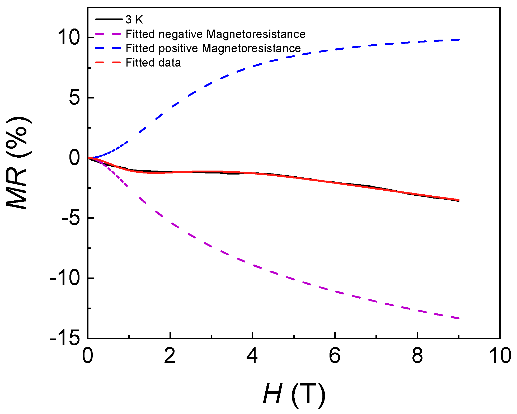
2. Results
3. Discussion
4. Conclusions
5. Methods
5.1. Preparation of a Re-Doped Graphene Device:
5.2. Transport Measurements
5.3. Raman Measurements
Author Contributions
Funding
Institutional Review Board Statement
Informed Consent Statement
Data Availability Statement
Acknowledgments
Conflicts of Interest
References
- Rein, M.; Richter, N.; Parvez, K.; Feng, X.; Sachdev, H.; Kläui, M.; Müllen, K. Magnetoresistance and Charge Transport in Graphene Governed by Nitrogen Dopants. ACS Nano 2015, 9, 1360–1366. [Google Scholar] [CrossRef] [PubMed]
- Ruan, H.; Guo, J.; Zhang, S.; Gao, Y.; Shang, W.; Liu, Y.; Su, M.; Liu, Y.; Wang, H.; Xie, T.; et al. In Situ Local Band Engineering of Monolayer Graphene Using Triboelectric Plasma. Small 2024, 20, 2309318. [Google Scholar] [CrossRef] [PubMed]
- Novoselov, K.S.; Geim, A.K.; Morozov, S.V.; Jiang, D.; Zhang, Y.; Dubonos, S.V.; Grigorieva, I.V.; Firsov, A.A. Electric field effect in atomically thin carbon films. Science 2004, 306, 666–669. [Google Scholar] [CrossRef] [PubMed]
- Bakalis, J.; Chernov, S.; Li, Z.; Kunin, A.; Withers, Z.H.; Cheng, S.; Adler, A.; Zhao, P.; Corder, C.; White, M.G.; et al. Momentum-Space Observation of Optically Excited Nonthermal Electrons in Graphene with Persistent Pseudospin Polarization. Nano Lett. 2024, 24, 9353–9359. [Google Scholar] [CrossRef]
- Hikami, S.; Larkin, A.I.; Nagaoka, Y. Spin-Orbit Interaction and Magnetoresistance in the Two Dimensional Random System. Prog. Theor. Phys. 1980, 63, 707–710. [Google Scholar] [CrossRef]
- Chen, A.; Maciejko, J.; Boettcher, I. Anderson Localization Transition in Disordered Hyperbolic Lattices. Phys. Rev. Lett. 2024, 133, 066101. [Google Scholar] [CrossRef]
- Aleiner, I.L.; Efetov, K.B. Effect of Disorder on Transport in Graphene. Phys. Rev. Lett. 2006, 97, 236801. [Google Scholar] [CrossRef]
- Altland, A. Low-Energy Theory of Disordered Graphene. Phys. Rev. Lett. 2006, 97, 236802. [Google Scholar] [CrossRef]
- McCann, E.; Kechedzhi, K.; Fal’ko, V.I.; Suzuura, H.; Ando, T.; Altshuler, B.L. Weak-Localization Magnetoresistance and Valley Symmetry in Graphene. Phys. Rev. Lett. 2006, 97, 146805. [Google Scholar] [CrossRef]
- Morpurgo, A.F.; Guinea, F. Intervalley Scattering, Long-Range Disorder, and Effective Time-Reversal Symmetry Breaking in Graphene. Phys. Rev. Lett. 2006, 97, 196804. [Google Scholar] [CrossRef]
- Ostrovsky, P.M.; Gornyi, I.V.; Mirlin, A.D. Electron transport in disordered graphene. Phys. Rev. B 2006, 74, 235443. [Google Scholar] [CrossRef]
- Chen, J.H.; Jang, C.; Adam, S.; Fuhrer, M.S.; Williams, E.D.; Ishigami, M. Charged-impurity scattering in graphene. Nat. Phys. 2008, 4, 377–381. [Google Scholar] [CrossRef]
- Chen, J.-H.; Cullen, W.G.; Jang, C.; Fuhrer, M.S.; Williams, E.D. Defect Scattering in Graphene. Phys. Rev. Lett. 2009, 102, 236805. [Google Scholar] [CrossRef] [PubMed]
- Li, X.; Sagar, R.U.R.; Zhong, L.; Liu, Y.; Hui, D.; Zhang, M. Nonsaturating negative magnetoresistance in laser-induced graphene. Mater. Lett. 2019, 248, 43–47. [Google Scholar] [CrossRef]
- Zeng, J.; Ma, P.C.; Zhang, S.X.; Xu, L.J.; Li, Z.Z.; Zhai, P.F.; Hu, P.P.; Maaz, K.; Sun, Y.M.; Liu, J. Unrecovered ion-irradiated damage after thermal annealing in graphene field effect transistors. Appl. Surf. Sci. 2022, 588, 153005. [Google Scholar] [CrossRef]
- Muszynski, R.; Seger, B.; Kamat, P.V. Decorating Graphene Sheets with Gold Nanoparticles. J Phys. Chem. C 2008, 112, 5263–5266. [Google Scholar] [CrossRef]
- Zhang, W.; van Dijk, B.; Wu, L.; Maheu, C.; Tudor, V.; Hofmann, J.P.; Jiang, L.; Hetterscheid, D.; Schneider, G.F. Role of Vacancy Defects and Nitrogen Dopants for the Reduction of Oxygen on Graphene. ACS Catal. 2024, 14, 11065–11075. [Google Scholar] [CrossRef]
- Williams, G.; Seger, B.; Kamat, P.V. TiO2-Graphene Nanocomposites. UV-Assisted Photocatalytic Reduction of Graphene Oxide. ACS Nano 2008, 2, 1487–1491. [Google Scholar] [CrossRef]
- Zhang, Y.; Wang, W.; Huang, M.; Liu, P.; Hu, G.; Feng, C.; Lei, X.; Gu, M.; Yang, H.; Liu, K.; et al. MnPS3 spin-flop transition-induced anomalous Hall effect in graphite flake via van der Waals proximity coupling. Nanoscale 2020, 12, 23266–23273. [Google Scholar] [CrossRef]
- Wang, Z.; Tang, C.; Sachs, R.; Barlas, Y.; Shi, J. Proximity-Induced Ferromagnetism in Graphene Revealed by the Anomalous Hall Effect. Phys. Rev. Lett. 2015, 114, 016603. [Google Scholar] [CrossRef]
- Wang, Y.; Luo, X.; Tseng, L.; Ao, Z.; Li, T.; Xing, G.; Bao, N.; Suzukiis, K.; Ding, J.; Li, S.; et al. Ferromagnetism and Crossover of Positive Magnetoresistance to Negative Magnetoresistance in Na-Doped ZnO. Chem. Mater. 2015, 27, 1285–1291. [Google Scholar] [CrossRef]
- Majumder, C.; Bhattacharya, S.; Saha, S.K. Anomalous large negative magnetoresistance in transition-metal decorated graphene: Evidence for electron-hole puddles. Phys. Rev. B 2019, 99, 045408. [Google Scholar] [CrossRef]
- Li, W.; He, Y.; Wang, L.; Ding, G.; Zhang, Z.; Lortz, R.W.; Sheng, P.; Wang, N. Electron localization in metal-decorated graphene. Phys. Rev. B 2019, 84, 045431. [Google Scholar] [CrossRef]
- Rehman Sagar, R.U.; Shehzad, K.; Ali, A.; Stadler, F.J.; Khan, Q.; Zhao, J.; Wang, X.; Zhang, M. Defect-induced, temperature-independent, tunable magnetoresistance of partially fluorinated graphene foam. Carbon 2019, 143, 179–188. [Google Scholar] [CrossRef]
- Zhou, Y.-B.; Han, B.-H.; Liao, Z.-M.; Wu, H.-C.; Yu, D.-P. From positive to negative magnetoresistance in graphene with increasing disorder. Appl. Phys. Lett. 2011, 98, 222502. [Google Scholar] [CrossRef]
- Rappoport, T.G.; Uchoa, B.; Castro Neto, A.H. Magnetism and magnetotransport in disordered graphene. Phys. Rev. B 2009, 80, 245408. [Google Scholar] [CrossRef]
- Khosla, R.P.; Fischer, J.R. Magnetoresistance in Degenerate CdS: Localized Magnetic Moments. Phys. Rev. B 1970, 2, 4084–4097. [Google Scholar] [CrossRef]
- Takiguchi, K.; Anh, L.D.; Chiba, T.; Koyama, T.; Chiba, D.; Tanaka, M. Giant gate-controlled proximity magnetoresistance in semiconductor-based ferromagnetic–non-magnetic bilayers. Nat. Phys. 2019, 15, 1134–1139. [Google Scholar] [CrossRef]
- Hong, X.; Cheng, S.H.; Herding, C.; Zhu, J. Colossal negative magnetoresistance in dilute fluorinated graphene. Phys. Rev. B 2011, 83, 085410. [Google Scholar] [CrossRef]
- Mayorov, A.S.; Gorbachev, R.V.; Morozov, S.V.; Britnell, L.; Jalil, R.; Ponomarenko, L.A.; Blake, P.; Novoselov, K.S.; Watanabe, K.; Taniguchi, T.; et al. Micrometer-Scale Ballistic Transport in Encapsulated Graphene at Room Temperature. Nano Lett. 2011, 11, 2396–2399. [Google Scholar] [CrossRef]
- Zhang, Y.; Wang, S.; Hu, G.; Huang, H.; Zheng, B.; Zhou, Y.; Feng, Y.; Ma, X.; He, J.; Lu, Y.; et al. Giant Carrier Mobility in Graphene with Enhanced Shubnikov–de Haas Quantum Oscillations: Implications for Low-Power-Consumption Device Applications. ACS Appl. Nano Mater. 2022, 5, 10860–10866. [Google Scholar] [CrossRef]


Disclaimer/Publisher’s Note: The statements, opinions and data contained in all publications are solely those of the individual author(s) and contributor(s) and not of MDPI and/or the editor(s). MDPI and/or the editor(s) disclaim responsibility for any injury to people or property resulting from any ideas, methods, instructions or products referred to in the content. |
© 2025 by the authors. Licensee MDPI, Basel, Switzerland. This article is an open access article distributed under the terms and conditions of the Creative Commons Attribution (CC BY) license (https://creativecommons.org/licenses/by/4.0/).
Share and Cite
Zhang, Y.; You, J.; Li, W.; Huang, Z.; Feng, Y.; Liu, Y.; Li, J. Rhenium-Induced Negative Magnetoresistance in Monolayer Graphene. Magnetochemistry 2025, 11, 39. https://doi.org/10.3390/magnetochemistry11050039
Zhang Y, You J, Li W, Huang Z, Feng Y, Liu Y, Li J. Rhenium-Induced Negative Magnetoresistance in Monolayer Graphene. Magnetochemistry. 2025; 11(5):39. https://doi.org/10.3390/magnetochemistry11050039
Chicago/Turabian StyleZhang, Ying, Jiali You, Weiwei Li, Zijie Huang, Yuxiang Feng, Yuyu Liu, and Jing Li. 2025. "Rhenium-Induced Negative Magnetoresistance in Monolayer Graphene" Magnetochemistry 11, no. 5: 39. https://doi.org/10.3390/magnetochemistry11050039
APA StyleZhang, Y., You, J., Li, W., Huang, Z., Feng, Y., Liu, Y., & Li, J. (2025). Rhenium-Induced Negative Magnetoresistance in Monolayer Graphene. Magnetochemistry, 11(5), 39. https://doi.org/10.3390/magnetochemistry11050039