Article

Hands-On Quantum Sensing with NV Centers in Diamonds

1
IMDEA Nanociencia, Faraday, 9, 28049 Madrid, Spain
2
Facultad de Ciencias, Universidad Autónoma de Madrid, 28049 Madrid, Spain
*
Author to whom correspondence should be addressed.
Submission received: 14 November 2022 / Revised: 16 December 2022 / Accepted: 18 December 2022 / Published: 29 January 2023

Abstract

:
The physical properties of diamond crystals, such as color or electrical conductivity, can be controlled via impurities. In particular, when doped with nitrogen, optically active nitrogen-vacancy centers ( N V ), can be induced. The center is an outstanding quantum spin system that enables, under ambient conditions, optical initialization, readout, and coherent microwave control with applications in sensing and quantum information. Under optical and radio frequency excitation, the Zeeman splitting of the degenerate states allows the quantitative measurement of external magnetic fields with high sensitivity. This study provides a pedagogical introduction to the properties of the N V centers as well as a step-by-step process to develop and test a simple magnetic quantum sensor based on color centers with significant potential for the development of highly compact multisensor systems.

1. Introduction

The word diamond comes from the Greek “adamantem” which means “invincible”. The diamond is an electrical insulator with strong covalent bonds that make it a material with extraordinary hardness, broadband optical transparency, and extremely high thermal conductivity. In addition, it can withstand large electric fields and, when doped, behaves like a semiconductor.
Diamonds are associated with the idea of perfection. However they are rarely perfect, and lattice irregularities or impurities are very common. By using artificial growth techniques, the nature and density of impurities can be controlled. This alters their physical properties, such as color or electrical conductivity. Optically active defects are called color centers.
In the N V color center, a nitrogen atom substitutes a carbon atom and a vacancy, in one of four adjacent positions, replaces another carbon atom. In this configuration, one electron is unpaired and remains trapped inside the vacancy. The center is charged negatively when it captures an additional electron, usually from a nitrogen atom donor in the lattice. The spin state of the two-electron quantum system can be controlled by using microwave pulses and optically addressed by measuring the photoluminescence [1].
All this, together with the long coherence time of the quantum state, and possibility of working at room temperature, makes them an ideal physical platform for the development of a magnetic sensor with unprecedented performance.
The spin orientation of the two electrons trapped inside the center is aligned with the axis of symmetry (the line joining the vacancy and the nitrogen).
Under a laser light illumination pulse in the range of 465 nm to 565 nm, the center fluoresces, emitting a photon in the red spectrum. When excited with microwaves, the fluorescence changes in such a way that it is possible to determine the external magnetic field [2].
Current technologies providing a high magnetic sensitivity, such as optical pumped magnetometry (OPM) [3], superconducting quantum interference devices (SQUID) [4], microelectromechanical systems (MEMS) [5], and magnetic resonance force microscopy (MRFM) [6], are highly successful technologies that have made possible the measurement of the magnetic field generated by neuronal activity with great precision. These systems have been previously described and compared [7].
A SQUID is based on superconducting loops containing Josephson junctions [8]. It is a very sensitive magnetometer used to measure extremely small magnetic fields, sensitive enough to measure fields as low as 5 × 10 14 T with a noise equivalent field of approximately 3 fT·Hz 1 / 2 . For the sake of comparison, it is important to notice that a common, small neodymium magnet produces a magnetic field of about 10 2 T, and neural activity in animals produces magnetic fields between 10 6 T and 10 9 T. Spin exchange relaxation-free (SERF) magnetometers measure magnetic fields by using lasers to detect the interaction of the magnetic field with alkali metal atoms in a vapor. They are potentially more sensitive and do not require cryogenic refrigeration but are orders of magnitude larger in size (1 cm 3 ).
SQUID requires cryogenics, OPM reduces the sensitivity when the device reduces its dimension [9] due to the atomic collisions that alter the spin, and they require operation in a near-zero magnetic field; consequently, the ambient 50 μ T Earth magnetic field must be properly screened. These technologies show limitations for miniaturization, because they either require special conditions and bulky instrumentation or their temporal resolution decreases when trying to reduce their dimensions.
In contrast, the quantum state of a color center in a diamond can be read out optically because the fluorescence is spin dependent, allowing its use in high-precision magnetometry at room temperature [10,11] and under an ambient magnetic field, such as the Earth’s magnetic field. Its properties have demonstrated temporal resolution [12] and ultrahigh sensitivity [13] to measure fields as low as 10 12 T [14] while allowing device miniaturization down to the millimeter, micrometer, or even the nanoscale.
The crystal structure of diamond consists of tetrahedral covalent bonds between an atom and its four nearest neighbors, linked in a face-centered cubic Bravais lattice. This strongly bonded, tightly packed, dense, and rigid structure gives rise to its outstanding properties.
An N V center [15] is a point defect in a diamond with an axial, trigonal C 3 v [16] symmetry [17] (three vertical reflection planes, and two 120 ° rotations about the Z axis), caused by a nitrogen impurity. The center has three possible configurations, a positive charge N V + , a neutral N V 0 (Figure 1a), and a negative charge N V (Figure 1d). These states have been well studied: N V + is nonfluorescent, N V 0 [18,19] has only one electron unpaired, is paramagnetic, and its luminescence intensity is lower than in the case of N V . The N V occurs when the center captures an additional electron, normally from a nitrogen donor in the lattice, and they form a pair with an integer quantum spin number of 0 or ± 1 , and it is the one used for magnetometry [20].
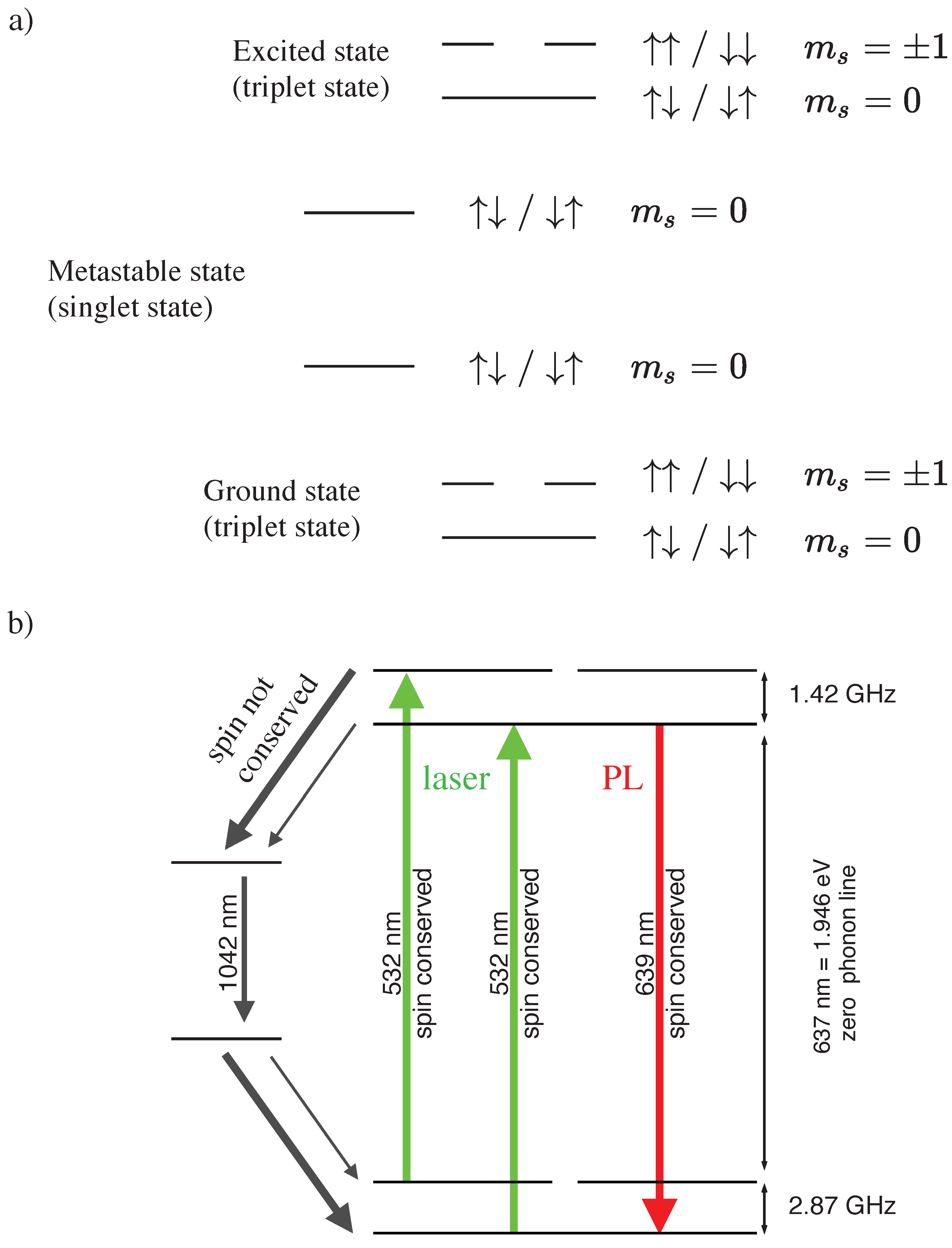
The electronic structure of the center (Figure 2) consists of a triplet ground state, a triplet excited state and two singlet states [21]. In the singlet state the spins are anti-aligned (up-down or down-up with m s = 0 ). In the triplet state, the spins can be aligned (up-up with m s = + 1 or down-down with m s = 1 ) or anti-aligned (with m s = 0 ). The state with the spins aligned is degenerated and requires more energy due to the electron-electron magnetic interaction.
Magnetometry under ambient conditions with color centers in a diamond is based on the optical measurement of the eigenvalues of the two-spin Hamiltonian of the electrons trapped in the center under the application of an external magnetic field. The measurement can be performed optically because the m s = ± 1 degenerated states preferentially follow a nonradiative path through the metastable singlet states, resulting in a reduction in the observed photoluminescence [23] compared to that corresponding to the m s = 0 state. Spin-state initialization [24] is achieved by applying properly tuned laser light, which causes optical pumping to the m s = 0 state. The microwave radiation at the resonance frequency populates the m s = ± 1 states that, under an external magnetic field, will split, giving rise to a decrease in the PL observed at the resonance frequencies.
If the center is shined on with laser light (we used a 532-nm or 2.33-eV, diode-pumped solid-state laser), the electrons are excited from the ground to the excited state, where these transitions are predominantly spin-conserving. The electrons immediately decay to the ground state and emit a photon of a lower frequency (red color); this photoluminescence (PL) is more intense when the center is in the m s = 0 state because the transition is closed (from m s = 0 ground state to the m s = 0 excited state and then back again to m s = 0 ground state). In the case of m s = ± 1 , the excitement conserves the spin but not the decay because one of the electrons flips and the state changes to m s = 0 , decaying through the metastable singlet states and emitting a photon in an infrared frequency [25], and therefore reducing the observed PL.
In a continuous optical excitation shining with a laser (465 nm to 565 nm in range) [26], the electron population, initially in the m s = ± 1 state, is pumped to the m s = 0 state; this is the method by which to initialize the system, with all the electrons set on the m s = 0 state.
In this situation, it is not possible to observe the effect of an external magnetic field on the PL because the degenerated states m s = ± 1 are not populated. Applying a microwave radiation at the 2.87 GHz resonance frequency, the m s = ± 1 ground states are populated again, allowing the excitement to the m s = ± 1 excited states and the subsequent decay through the nonradiative route showing a decrease in the PL.
Under this continuous microwave radiation, applying an external magnetic field with strength B 0 , the magnetic moment of the electron aligns itself as either antiparallel ( m s = 1 ) to the magnetic field component corresponding to the N V axis, with a specific energy level, or parallel ( m s = + 1 ) with a different energy, due to the Zeeman shift of the spin sublevels. Therefore, now, the PL decreases at two different resonance frequencies. This separation of the sublevels is linear and proportional to the applied magnetic field component corresponding to the NV axis and produces a decrease in the observed PL at those frequencies. Increasing the magnetic field and due to the hyperfine structure and different orientations of different N V centers, other levels are also split and different dips on the PL are observed.

2. Materials and Methods

Color centers in diamonds can be characterized experimentally by using [27,28] optically detected magnetic resonance (ODMR) or electron spin resonance (ESR) techniques together with the photoluminescence signal emitted during the relaxation of an excited state to its ground state. In this study, ODMR is used for the characterization of the color centers in diamonds.
Throughout this research and for all the experiments, two synthetic-type Ib diamond samples have been used, manufactured using the high-pressure, high-temperature (HPHT) synthesis process by the supplier element6 [29]. The luminescence has been studied by using such samples for a set of N V centers in which each N V axis is randomly oriented in the four possible directions.
It is important, for nanoscale applications, that the centers are located as close to the surface as possible. Type Ib diamonds are artificially fabricated [30] to contain up to 500 ppm nitrogen, absorb green light, and have a dark yellow or brown color. The samples used in our investigation have a central NV concentration of approximately 1 ppm .
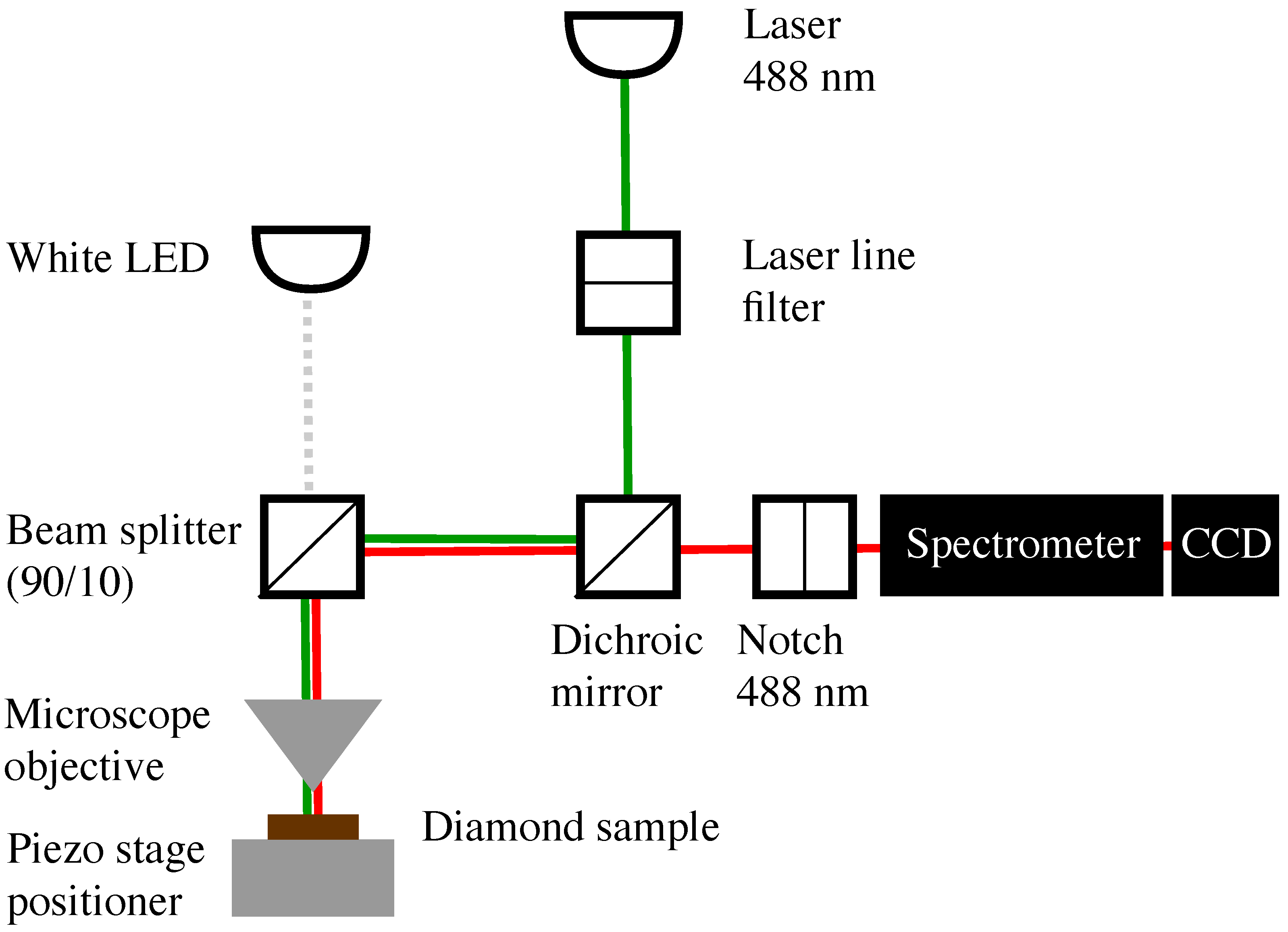
With the sensor as the final target, the first step is the characterization of the two diamonds, developed for quantum sensing purposes. Both samples—the polycrystalline and the single crystal—have been characterized under ambient conditions by using a 488 nm wavelength argon ion laser in a low vibration optical setup (Figure 3), achieving almost identical results in PL intensity and peaks observed.

3. Results and Discussion

3.1. Optical Characterization

At low power, the PL intensity is linear to the excitation power, and at high power it may reach saturation. Due to the vibrational and rotational effects on atomic levels, emission does not occur at a single wavelength but in a range from 600 nm to 800 nm. The photoluminescence spectra (Figure 4) shows the four characteristic frequency peaks: the N V zero phonon line (ZPL) at 637 nm , the N V 0 ZPL at 576 nm and the wide phonon sideband with two visible peaks at 662 nm and 684 nm [27]. A small Raman peak corresponding to the vibration of the sp 3 (tetrahedral) diamond lattice was also identified.
The mentioned zero-phonon line and the phonon sidebands constitute the spectra of the single-color centers in diamond-absorbing and emitting light. For the ensemble of color centers, each N V center contributes with a zero-phonon line and a phonon sideband to the total absorption and emission spectra, which is considered not homogeneously broadened because each N V center is surrounded by a different environment in the lattice, which modifies in a different way the energy required for an electronic transition, shifting and overlapping each zero phonon and vibrionic phonon sideband positions [31].
The zero-phonon line is located at a frequency determined by the energy gap between the N V center ground and excited state and also determined by the local environment. The phonon sideband is shifted to a higher frequency in absorption and to a lower frequency in fluorescence (see Appendix B. Characterization details).

3.2. Optically Detected Magnetic Resonance (ODMR)

Because the magnetic field is detected optically through the splitting of the degenerated states due to the Zeeman effect, the next step in the process requires the m s = ± 1 center state populated. For that purpose the setup is extended by adding a microwave source and a resonator.
As shown before, by continuously applying laser light ( 532 nm diode), the electrons in the centers are pumped to the m s = 0 ground state (Figure 2). By applying a resonant microwave field with an energy of 2.87 GHz , corresponding to the gap between the quantum levels m s = 0 and m s = ± 1 , the electrons in the center are excited to the m s = ± 1 state.
The comparative measurement of the 1042 nm transition, by applying or not applying the resonant microwave field under continuous laser excitation, allows the detection of the PL attenuation, due to the greater absorption in the infrared frequency that occurs in the transition between the singlet states as well as the long coherence time of those singlet states ( N V centers inhomogeneous spin relaxation time was assessed to be in the order of 300 ns , [32,33]). When the microwave field is retired, the electrons return to the m s = 0 state and therefore that transition does not take place, resulting in an increase in the photoluminescence.
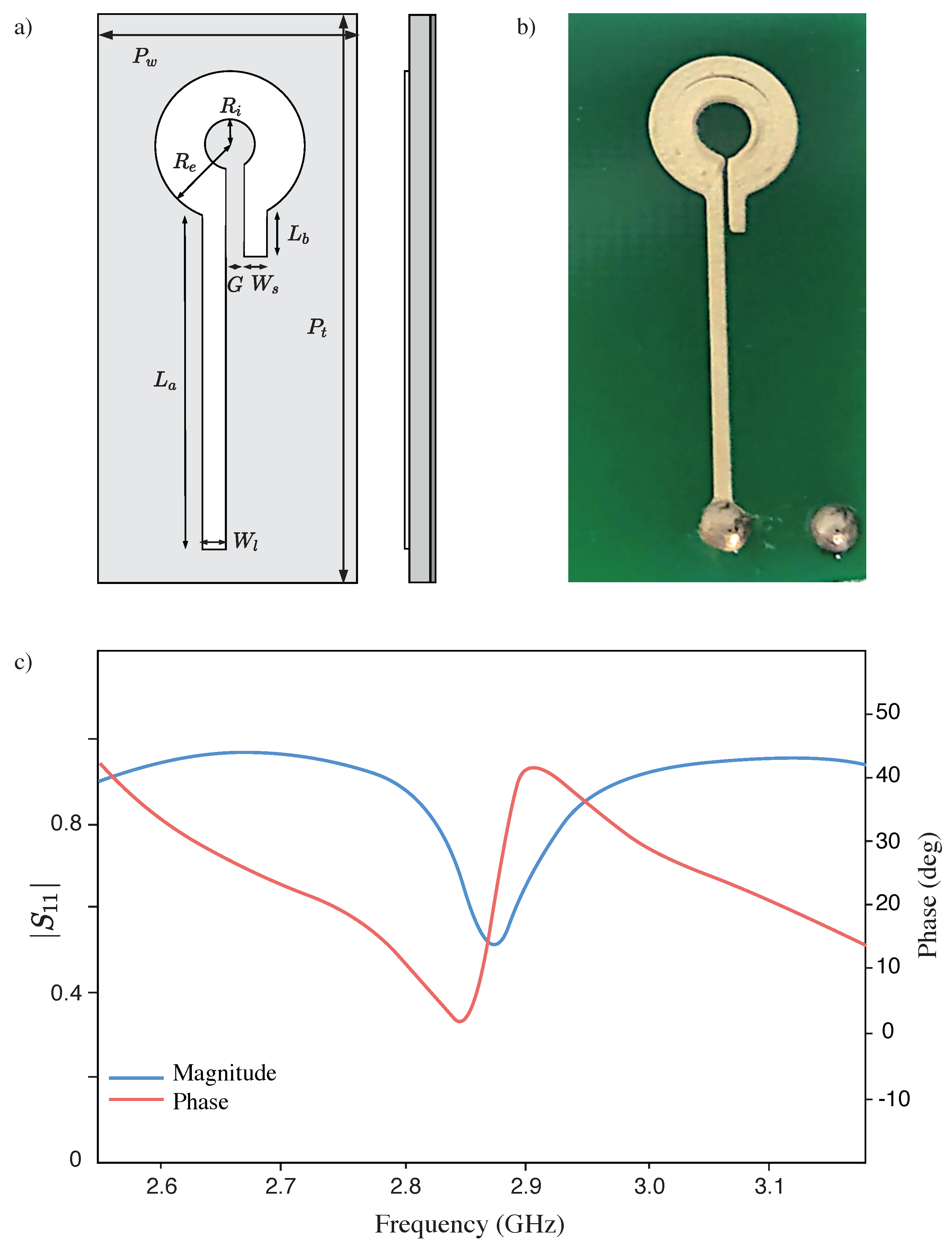
To irradiate the diamond with microwaves pulses, the research team manufactured a resonator with the topology and characteristics described in Figure 5, based on a previous design by Man Zhao et al. [34] and the study of Eisuke Abe et al. [35] by silver printing on a PCB by using a Voltera V-One PCB printer [36].
The diamond sits on top of the resonator. The resonator generates a spatially uniform and concentrated field over an area of approximately 1 mm 2 with a resonance frequency of 2.87 GHz and a bandwidth of 100 MHz , permitting it to work with different resonances generated by the hyperfine structure.

3.3. Photoluminescence Intensity in Proportion to the Applied Microwave Frequency

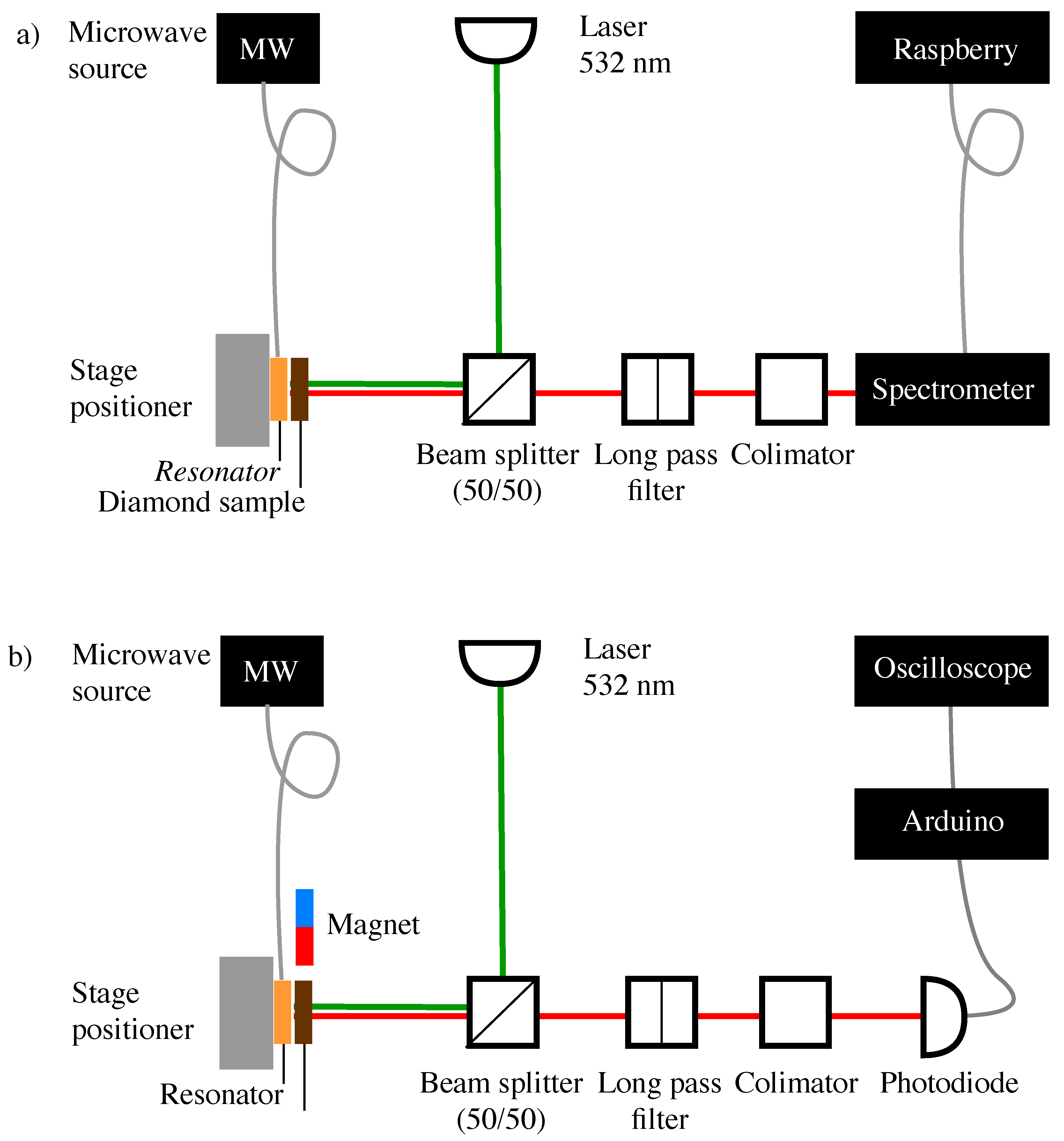
The new experimental setup (Figure 6a) includes a microwave source, a spectrometer, and a computer to process the signal (all of them detailed in Appendix A. Component detail), allowed us to visualize the effect of the microwaves in the PL
For this study we programmed the microwave (MW) source to sweep [37] in a range of frequencies from 2.7 GHz to 3.0 GHz (10 MHz step; 5.0 dBm constant power; 26 s sweep duration) and a code to integrate the total luminescence detected by the spectrometer per time unit ( 100 ms integration time).
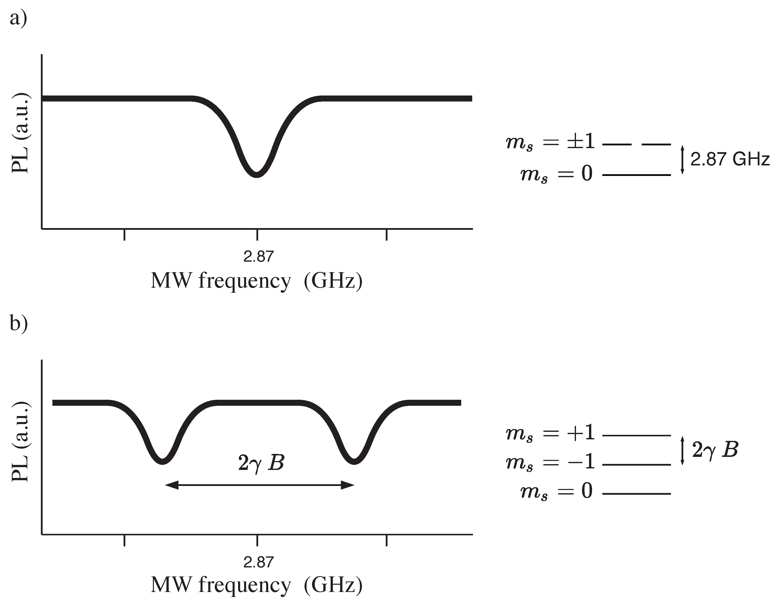
As predicted by the theory, we observed a dip right at the resonance frequency of 2.87 GHz .
Under the laser beam (532 nm), the two electrons in the color center, are excited from the m s = 0 ground state to the m s = 0 excited state and then recombined again to the m s = 0 ground state. The microwaves have no effect except for the resonance frequency. At this frequency, the electrons absorb the energy from the MW pulse and populate the m s = ± 1 ground state; from that, the laser beam excites them to the m s = ± 1 excited state to finally decay through the spin nonconservative and nonradiative path across the metastable states, resulting in a reduced fluorescence signal (Figure 7a).
At this point, the research team was able to move forward and explore the effect of the magnetic field in the photoluminescence.

3.4. PL under an External Magnetic Field

The spin-triplet ground state has a zero field splitting at 2.87 GHz between m s = 0 and m s = ± 1 sublevels, splitting and shift of the levels appear due to electron spin–spin interaction [38]. Intersystem crossing (ISC), plays a key role in the excited state decay dynamics. It is the mechanism by which the center changes its spin state from excited state m s = ± 1 to the metastable m s = 0 .
Due to the higher ISC rate for the m s = ± 1 state under the laser light, the center is polarized to the m s = 0 state, being the lifetime for the m s = 0 excited state of 23 ns , and almost double the one corresponding to the m s = ± 1 excited state of 12.5 ns . The metastable state emits an infrared photon with a wavelength of 1046 nm and has a long lifetime of 300 ns , which is used to optically read the state of the center [39].
Considering the N V axis aligned with the Z-axis and an external magnetic field coupled to the center through the Zeeman effect, the triplet ground state has an effective spin Hamiltonian given by
H N V = D S Z 2 + γ e B · S ,
where D = 2.87 GHz is the zero field splitting, S represents the electron spin projection operator, γ e is the electron gyromagnetic ratio with a value of 28.0249 GHz / T , and B is the vector of the magnetic field.
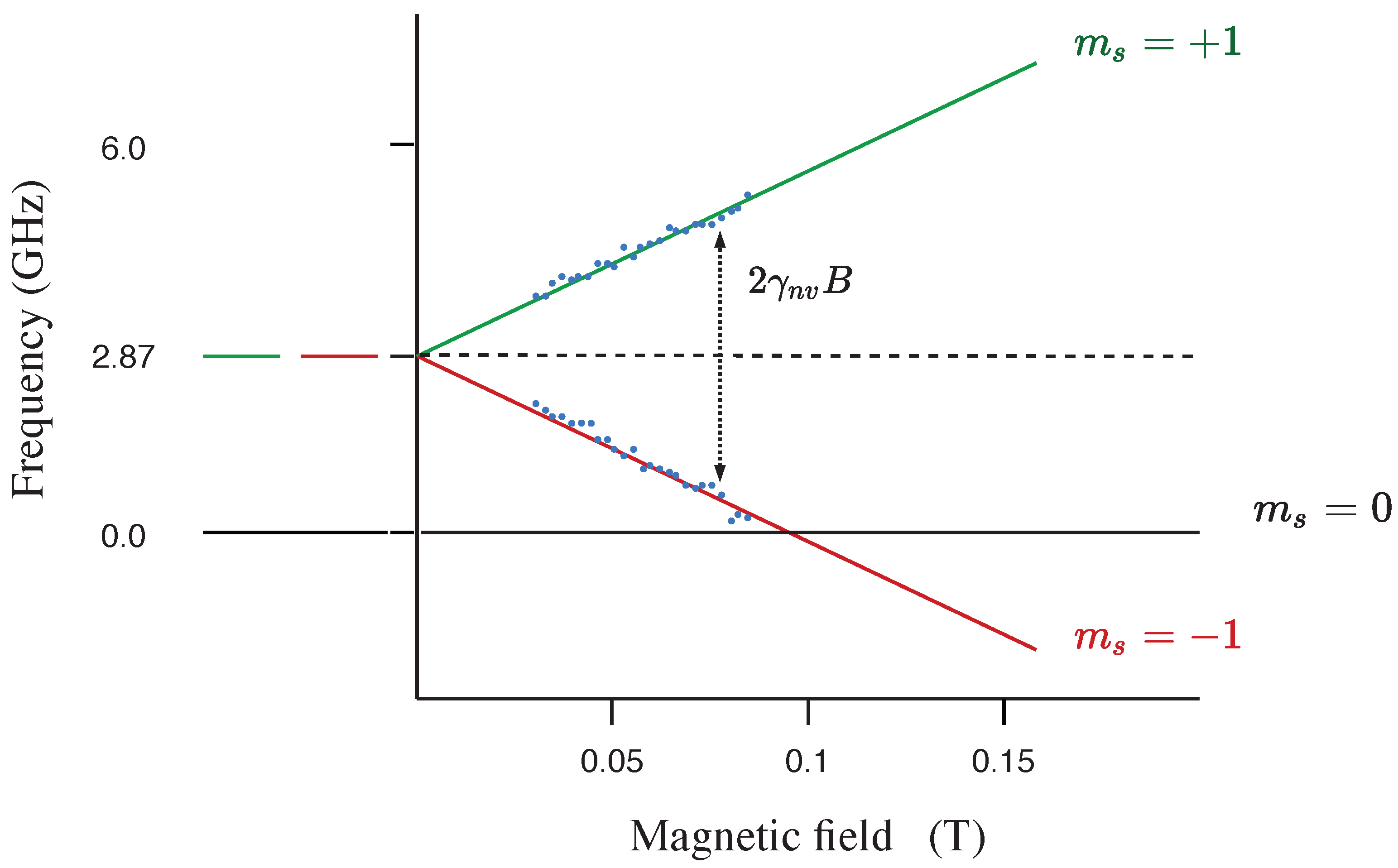
The magnetic field vector component aligned with the N V axis couples with the center, and then the gap between the energies of the degenerated states, initially the same energy at zero field, now separates linearly with the magnetic field by 2 γ e B and therefore, the effect can be used to measure the external magnetic field strength because the splitting of the energy levels is directly proportional to the strength of the applied magnetic field component aligned with the N V axis, as shown in Figure 8.
To continue the experiment, the experimental setup was extended by including an electromagnet placed close to the diamond as seen in Figure 4. The electromagnet was connected to a precision power supply that allowed us to vary the voltage and thus the external magnetic field that acted on the material. Then the process consisted of taking measurements of the observed PL for the different voltage values between 0 and 12 volts (blue dots in Figure 8).
Once having demontrated the control on the measurement of the magnetic field, it was possible to proceed with the steps toward improving the sensitivity and reduce the size of the device. For that purpose, a new setup, more compact and simplified, was designed to replace the spectrometer by a photodiode connected to an Arduino board to read the signal and visualize it on an oscilloscope (Figure 6b).
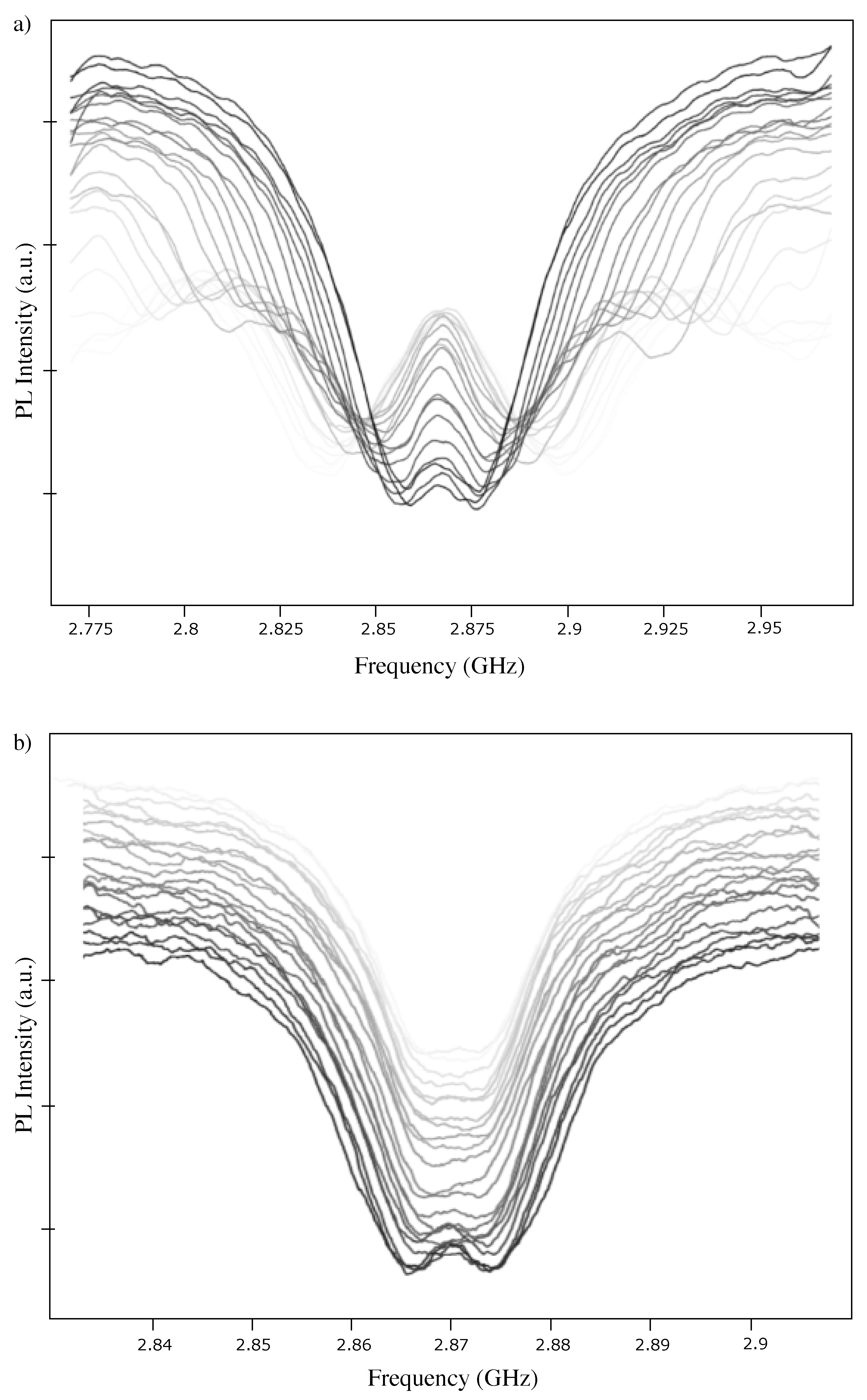
With this new setup, it was possible to represent in more detail the PL landscape in proportion to the microwave frequency and the magnetic field, producing the series represented in the Figure 9.
To more accurately measure the relationship between the magnetic field and the observed luminescence, the research team used a teslameter (FH-55 Teslameter [40]). The FH-55 tip probe was placed at the point where later the diamond would be placed; then, the value of the magnetic field, to the nearest hundredth of a millitesla, was recorded for each position of the magnet (moved at steps of 0.5 mm).
Once these measurements were collected, the study continued following the usual procedure, that is, first, shining with a 532-nm laser light to polarize the centers, leaving at least 30 min to ensure laser stabilization (otherwise, the observed PL could be displaced, although it would not affect dips separation as a result of the splitting). Then, once the system stabilizes, a frequency sweep was performed from 2.7 to 3.0 GHz for each of the magnetic field values, corresponding to a specific position of the magnet with respect of the diamond.
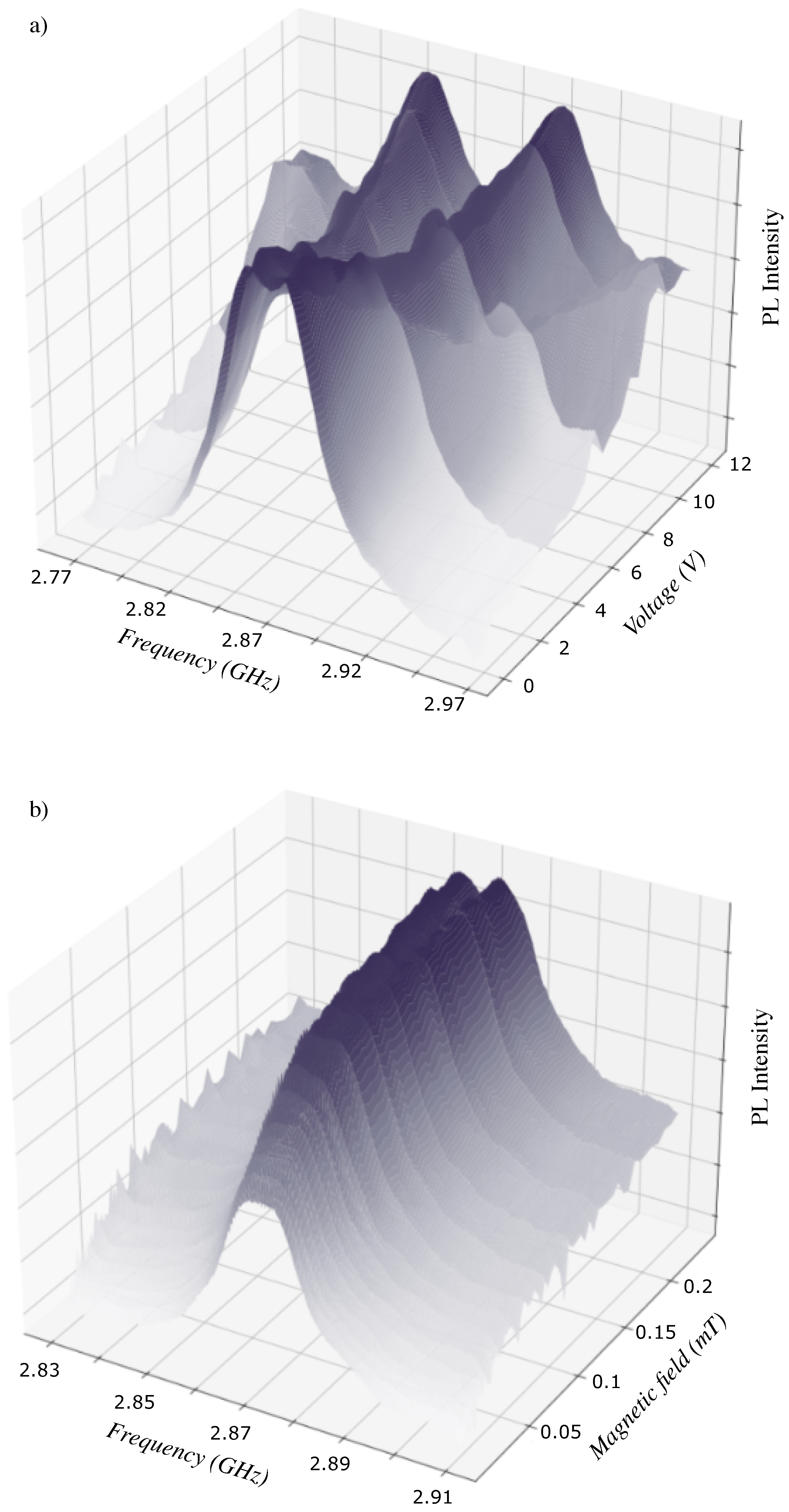
Figure 9 presents the results of the photoluminescence curves plotting intensity as a function of wavelength. Figure 9a shows the magnetic resonance spectra of the ensemble of N V centers corresponding to the 24 scans for different electromagnet voltage values between 0 and 12 volts, increasing 0.5 V at each step. In the figure, the darker the curve, the smaller the magnetic field. It can be seen how, with the increase of the magnetic field, the number of dips (corresponding to the transitions between the states m s = 0 and m s = ± 1 ) increases due to how the different possible orientations of the N V axis within the crystal structure perceive different projections of the magnetic field.
Figure 9b also presents the PL as a function of the frequency for magnetic field values, increasing at steps of 0.005 mT from 0.23 mT to 0.01 mT; in this case, the lighter the color of the curve, the lower the magnetic field.
In both cases, the pattern is clear because it shows the expected symmetry as a consequence of the Zeeman splitting, and the separation of the two global minima in the PL shows the linear dependence of the applied magnetic field and the distance between dips.
Finally, Figure 10a,b depicts the same data, but in a 3D representation combining PL intensity, magnetic field, and frequency.

4. Conclusions

In a series of experiments, two samples of commercially available synthetic Ib diamonds from element6 vendor, a polycrystalline diamond and a single crystal, have been used. These samples were grown by the high-pressure, high-temperature (HPHT) synthesis processes and characterized in a low-vibration optical setup showing the characteristic spectra of an ensemble of the N V centers, both N V 0 and N V , as well as the sidebands. The photoluminescence was represented as a function of wavelength, as well as its evolution in time under different conditions.
By using the previous material, the research team has prepared an experimental setup in order to initialize the system, pumping the electrons that form the color centers to the m s = 0 state, by applying laser light, observing the expected behavior.
The development of a resonator, specifically designed to emit at the resonance frequency, has made it possible to apply a microwave pulse to the diamond under continuous laser illumination. These conditions have repopulated the degenerated states m s = ± 1 making it possible to observe the decrease in the observed PL. This happens because the electrons follow the nonradiative decay path through the metastable state. The frequency sweep has verified the resonance frequency or energy gap between the states m s = 0 and m s = ± 1 . With this experimental setup, it has been possible not only to initialize the state but also to identify the resonance frequency and verify the evolution of the PL when applying microwave pulses, laying the groundwork for the next experiment.
In a last experiment, a magnetic field has been applied in a controlled way with the aim of measuring the displacement of the resonance frequencies due to the Zeeman effect and which constitutes the basis of magnetometry with color centers. The steps to develop this new setup, as well as the results, are also part of this work, leaving the way open to the miniaturization phase.

Author Contributions

J.L.S.T. conceived the idea, designed the experiments, acquired and analysed experimental data, and wrote the manuscript. V.M. participated in the acquisition of the PL and Raman measurements. R.B.-G. contributed to the design of the experiments, the use of instruments and helped with the attainment of experimental data. J.L.P. contributed to the idea and supervised the experimental findings. D.G. obtained financial support, managed the research team and contributed to the analysis of the experimental data. All the authors contributed to the editing of the final manuscript. All authors have read and agreed to the published version of the manuscript.

Funding

This research was funded by MICIN-AEI: Grants DETECTA ESP2017-86582-C4-3-R and EQC2018-005134-P Comunidad de Madrid: Grant TEC2SPACE-CM P2018/NMT-4291, ONR-G: G#N62909-19-1-2053 (DEFROST), MADE-MICINN: PID2019-105552RB-C44. Garantía Juvenil nº201701520868, R.B.-G. would like to thank Comunidad de Madrid for the funding through the grant 2019-T2/IND-13367.

Acknowledgments

We thank M.A. Ramos, G. García, N. Gordillo and A. Redondo from CMAM (Centre for Micro Analysis of Materials) for fruitful discussions on diamond characteristics and its possible modification by using ion irradiation in order to improve sensitivity. Matthew Markham from Element6 for providing the diamond samples. IMDEA Nanoscience nanofabrication facility, for assistance in many aspects, analysis of materials, and fabrication of some of the components.

Conflicts of Interest

The authors declare no conflict of interest.

Appendix A. Component Detail

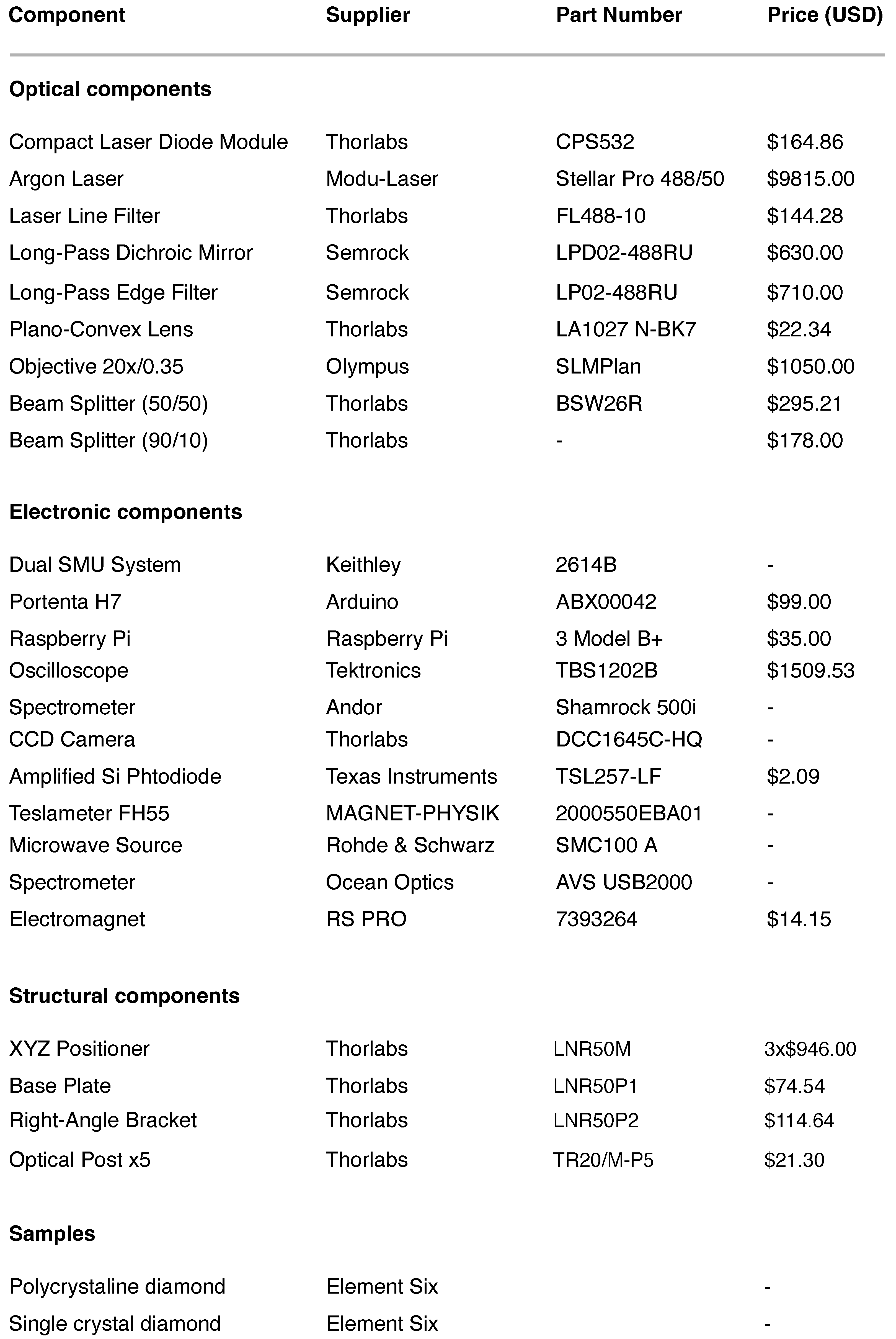
Figure A1 shows the list of components organized in four main blocks: optical components, including diodes, filters, lenses, splitters, and objectives; electronic components and instruments, including computers, oscilloscopes, spectrometers, CCD cameras, teslameter, microwaves sources, electromagnets and power supplies; structural components, including positioners, posts, brackets, and other elements; and finally the diamond samples used for the experiments.
The component name, the supplier, the part number when possible, and the approximate market price in USD.
Figure A1. List of components.
Carbon 09 00016 g0a1

Appendix B. Characterization Details
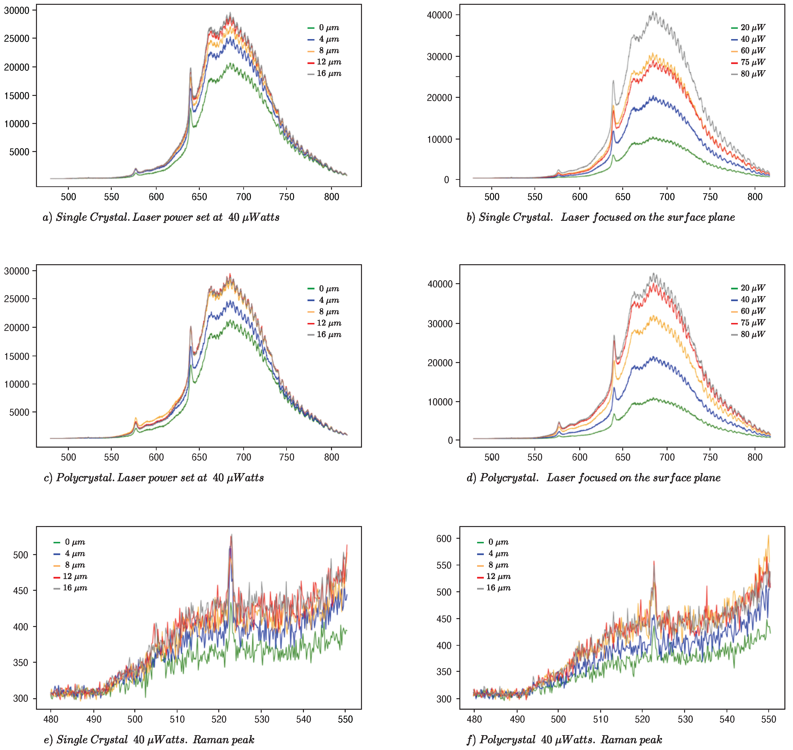
Figure A2 shows the photoluminescence spectra for an NV spin ensemble embedded in a single-crystal diamond (red) and a polycrystalline diamond (blue).
Figure A2. Photoluminescence spectra smoothed out for an NV spin ensemble.
Carbon 09 00016 g0a2
These curves show the typical luminescence representing the intensity as a function of the wavelength, highlighting the zero-phonon lines (ZPL) and the phonon sidebands.
NV and NV 0 centers can be optically distinguished by their different zero phonon lines at 639 nm and 575 nm , respectively. The NV zero-phonon line is determined by the intrinsic difference in energy levels between the spin triplet ground and excited states.
The NV phonon sideband is shifted to a higher frequency in absorption and to a lower frequency in fluorescence.
The two samples were characterized at room temperature under different conditions of laser light intensities and at different depths of focus with an integration time of 0.25 s, getting almost identical results. Specifically, Figure A3a shows the luminescence curve plotting intensity as a function of wavelength for the diamond single crystal.
In the setup, the objective can be translated upward or downward, changing the focus. The lines represent the spectra measured directly with focus on the surface (green), and the rest of the lines in blue, orange, red, and gray. Those measured focusing at the different depths—that is, 4 μ m, 8 μ m, 12 μ m and 16 μ m—are very similar. The greater the depth, the greater the observed intensity of the luminescence due to the volume of the stimulated material is greater and therefore, so is the number of activated centers. As a consequence, the number of emitted photons increases.
Similarly Figure A3b shows the luminescence curve plotting intensity as a function of wavelength for the diamond single crystal but, in this case, the lines represent the spectra measured for different laser intensities: 20 μ W (green line), 40 μ W (blue), 60 μ W (orange), 75 μ W (red) and 80 μ W (grey). In general, the greater the laser power, the greater the observed intensity of the luminescence because of the linearity between laser intensity and PL.
Figure A3c,d show results for the diamond polycrystalline sample, very similar to the ones from the single-crystal diamond.
The four Figure A3a–c show an oscillation after 650 nm due to the optical interference in the spectrometer sensor which is back illuminated.
Finally, Figure A3e,f show the zoom in the frequency range from 480 nm to 550 nm for the single-crystal and polycrystalline samples, respectively. In both cases, a small Raman peak corresponding to the vibration of the s p 3 diamond lattice [41] was observed at 523 nm or 1371 cm 1 .
Figure A3. Photoluminescence spectra for the single crystal (a,b) and detail of the observed Raman peak (e). Photoluminescence spectra for the polycrystal (c,d) and detail of the observed Raman peak (f).
Carbon 09 00016 g0a3

References

  1. Doherty, M.W.; Manson, N.B.; Delaney, P.; Jelezko, F.; Wrachtrup, J.; Hollenberg, L.C. The nitrogen-vacancy colour centre in diamond. Phys. Rep. 2013, 528, 1–45. [Google Scholar] [CrossRef] [Green Version]
  2. Taylor, J.M.; Cappellaro, P.; Childress, L.; Jiang, L.; Budker, D.; Hemmer, P.R. High-sensitivity diamond magnetometer with nanoscale resolution. Nat. Phys. 2008, 4, 810–816. [Google Scholar] [CrossRef]
  3. Dang, H.B.; Maloof, A.C.; Romalis, M.V. Ultrahigh sensitivity magnetic field and magnetization measurements with an atomic magnetometer. Appl. Phys. Lett. 2010, 97, 151110. [Google Scholar] [CrossRef] [Green Version]
  4. Drung, D.; Assmann, C.; Beyer, J.; Kirste, A.; Peters, M.; Ruede, F.; Schurig, T. Highly Sensitive and Easy-to-Use SQUID Sensors. IEEE Trans. Appl. Supercond. 2007, 17, 699–704. [Google Scholar] [CrossRef]
  5. Todaro, M.; Sileo, L.; Vittorio, M. Magnetic Field Sensors Based on Microelectromechanical Systems (MEMS) Technology. Magn. Sens. 2012. [Google Scholar] [CrossRef] [Green Version]
  6. Degen, C.; Poggio, M.; Mamin, H.; Rettner, C.; Rugar, D. Nanoscale magnetic resonance imaging. Proc. Natl. Acad. Sci. USA 2009, 106, 1313–1317. [Google Scholar] [CrossRef] [Green Version]
  7. Amir Borna, T.R.C. Non-Invasive Functional-Brain-Imaging with an OPM-based Magnetoencephalography System; Technical report; Sandia National Laboratories: Albuquerque, NM, USA, 2020. [Google Scholar]
  8. Khaneja, N. SQUID Magnetometers, Josephson Junctions, Confinement and BCS Theory of Superconductivity. In Magnetometers; Curilef, S., Ed.; IntechOpen: Rijeka, Croatia, 2019; Chapter 5. [Google Scholar] [CrossRef] [Green Version]
  9. Tierney, T.; Holmes, N.; Mellor, S. Optically pumped magnetometers: From quantum origins to multi-channel magnetoencephalography. NeuroImage 2019, 199, 598–608. [Google Scholar] [CrossRef]
  10. Degen, C.; Reinhard, F.; Cappellaro, P. Quantum sensing. Rev. Mod. Phys. 2017, 89, 035002. [Google Scholar] [CrossRef] [Green Version]
  11. Maze, J.; Stanwix, P.; Hodges, J.; Hong, S.; Taylor, J.; Cappellaro. Nanoscale magnetic sensing with an individual electronic spin in diamond. Nature 2008, 455, 644–647. [Google Scholar] [CrossRef]
  12. Hall, L.; Beart, G.; Thomas, E.; Simpson, D.; Mcguinness. High spatial and temporal resolution wide-field imaging of neuron activity using quantum NV-diamond. Sci. Rep. 2012, 2, 401. [Google Scholar] [CrossRef] [Green Version]
  13. Wolf, T.; Neumann, P.; Nakamura, K.; Sumiya, H.; Ohshima, T.; Isoya, J.; Wrachtrup, J. Subpicotesla Diamond Magnetometry. Phys. Rev. X 2015, 5, 041001. [Google Scholar] [CrossRef] [Green Version]
  14. Mitchell, M.W.; Alvarez, S.P. Quantum limits to the energy resolution of magnetic field sensors. Rev. Mod. Phys. 2020, 92, 21001. [Google Scholar] [CrossRef]
  15. Marcus, W.; Doherty, N.B.M. The Nitrogen-Vacancy Colour Centre in Diamond; Technical report; School of Physics, University of Melbourne: Melbourne, VIC, Australia, 2013. [Google Scholar]
  16. Wikipedia Contributors. Molecular symmetry Wikipedia, The Free Encyclopedia. 2022. Available online: https://en.wikipedia.org/w/index.php?title=Element_Six&oldid=1118487397 (accessed on 23 May 2022).
  17. Humphreys, J.; Liu, Q.; Humphreys, J.; Erne, R. A Course in Group Theory; Oxford Graduate Texts in Mathematics, Oxford University Press: Oxford, UK, 1996. [Google Scholar]
  18. Ferrari, A.M.; D’Amore, M.; El-Kelany, K.E.; Gentile, F.S.; Dovesi, R. The NV0 defects in diamond: A quantum mechanical characterization through its vibrational and Electron Paramagnetic Resonance spectroscopies. J. Phys. Chem. Solids 2022, 160, 110304. [Google Scholar] [CrossRef]
  19. Gali, A. Theory of the neutral nitrogen-vacancy center in diamond and its application to the realization of a qubit. Phys. Rev. B 2009, 79, 235210. [Google Scholar] [CrossRef]
  20. Kasper Jensen, P.K. Magnetometry with Nitrogen-Vacancy Centers in Diamond; Technical report; Niels Bohr Institute, University of Copenhagen: Copenhagen, Denmark, 2017. [Google Scholar]
  21. van Oort, E.; Glasbeek, M. Cross-relaxation dynamics of optically excited NV centers in diamond. Phys. Rev. B 1989, 40, 6509–6517. [Google Scholar] [CrossRef] [Green Version]
  22. Alkahtani, M.; Hemmer, P. Charge Stability of Nitrogen-Vacancy Color Center in Organic Nanodiamonds. Opt. Mater. Express 2020, 10. [Google Scholar] [CrossRef]
  23. Gaebel, T.; Domhan, M.; Wittmann, C. Photochromism in single nitrogen-vacancy defect in diamond. Appl. Phys. 2006, 455, 243–246. [Google Scholar] [CrossRef]
  24. Choi, S.; Jain, M.; Louie, S. Mechanism for optical initialization of spin in NV center in diamond. Phys. Rev. B 2012, 86, 041202. [Google Scholar] [CrossRef]
  25. Rogers, L.J.; Armstrong1, S.; Sellars, M.L.; Manson, N.B. New Infrared Emission of the NV Centre in Diamond: Zeeman and Uniaxial Stress Studies; Technical report; Laser Physics Center, Australian National University: Canberra, Australia, 2008. [Google Scholar]
  26. Robledo, L.; Bernien, H.; van Weperen, I.; Hanson, R. Control and Coherence of the Optical Transition of Single Nitrogen Vacancy Centers in Diamond. Phys. Rev. Lett. 2010, 105, 177403. [Google Scholar] [CrossRef]
  27. Subedi, S.D.; Fedorov, V.V.; Peppers, J.; Martyshkin, D.V.; Mirov, S.B.; Shao, L.; Loncar, M. Laser spectroscopic characterization of negatively charged nitrogen-vacancy (NV) centers in diamond. Opt. Mater. Express 2019, 9, 2076–2087. [Google Scholar] [CrossRef]
  28. Neumann, P.; Kolesov, R.; Jacques, V.; Beck, J. Excited-state spectroscopy of single NV defects in diamond using optically detected magnetic resonance. New J. Phys. 2009, 11, 013017. [Google Scholar] [CrossRef]
  29. Element Six. Synthetic Diamond and Tungsten Carbide Experts. 2022.
  30. Vavilov, V.S. The properties of natural and synthetic diamond. Physics-Uspekhi 1993, 36, 1083–1084. [Google Scholar] [CrossRef]
  31. Jelezko, F.; Wrachtrup, J. Single Defect Centres in Diamond: A Review; Technical report; DPhysikalisches Institut, Universität Stuttgart: Stuttgart, Germany, 2006. [Google Scholar]
  32. Childress, L.; Dutt, M.G.; Taylor, J.M.; Zibrov, A.S.; Jelezko, F. Coherent Dynamics of Coupled Electron and Nuclear Spin Qubits in Diamond. Science 2006, 314, 281–285. [Google Scholar] [CrossRef] [Green Version]
  33. Trofimov, S.D.; Tarelkin, S.A.; Bolshedvorskii, S.V. Spatially controlled fabrication of single NV centers in IIa HPHT diamond. Opt. Mater. Express 2020, 10, 198–207. [Google Scholar] [CrossRef] [Green Version]
  34. Man Zhao, Q.L. Antenna for Microwave Manipulation of NV Colour Centres; Technical report; The Institution of Engineering and Technology: London, UK, 2020. [Google Scholar]
  35. Eisuke Abe, K.S. Tutorial: Magnetic Resonance with Nitrogen-Vacancy Centers in Diamond Microwave Engineering, Materials Science, and Magnetometry; Technical report; Spintronics Research Center, Keio University: Tokyo, Japan, 2018. [Google Scholar]
  36. Voltera v-one PCB Printer. 2022. Available online: https://www.voltera.io/store/v-one (accessed on 24 July 2022).
  37. Maria Simanovskaia, K.J. Sidebands in Optically Detected Magnetic Resonance Signals of Nitrogen Vacancy Centers in Diamond; Technical report; Department of Physics, University of California: Berkeley, CA, USA, 2013. [Google Scholar]
  38. Harrison, J.; Sellars, M.; Manson, N. Optical spin polarisation of the N-V centre in diamond. J. Lumin. 2004, 107, 245–248. [Google Scholar] [CrossRef]
  39. Rogers, L.; Jahnke, K.; Metsch, M.; Sipahigil, A.; Binder, J.; Teraji. All-Optical Initialization, Readout, and Coherent Preparation of Single Silicon-Vacancy Spins in Diamond. Phys. Rev. Lett. 2014, 113, 263602. [Google Scholar] [CrossRef] [Green Version]
  40. Magnetic Field Strength Meter Gauss-/Teslameter FH 55. 2022. Available online: https://www.magnet-physik.de/upload/31925018-FH-55-e-3157.pdf (accessed on 24 July 2022).
  41. Gilkes, K.; Prawer, S.; Nugent, K.; Robertson, J.; Sands, H.; Lifshitz, Y.; Shi, X. Direct quantitative detection of the sp3 bonding in diamond-like carbon films using ultraviolet and visible Raman spectroscopy. J. Appl. Phys. 2000, 87, 7283–7289. [Google Scholar] [CrossRef]
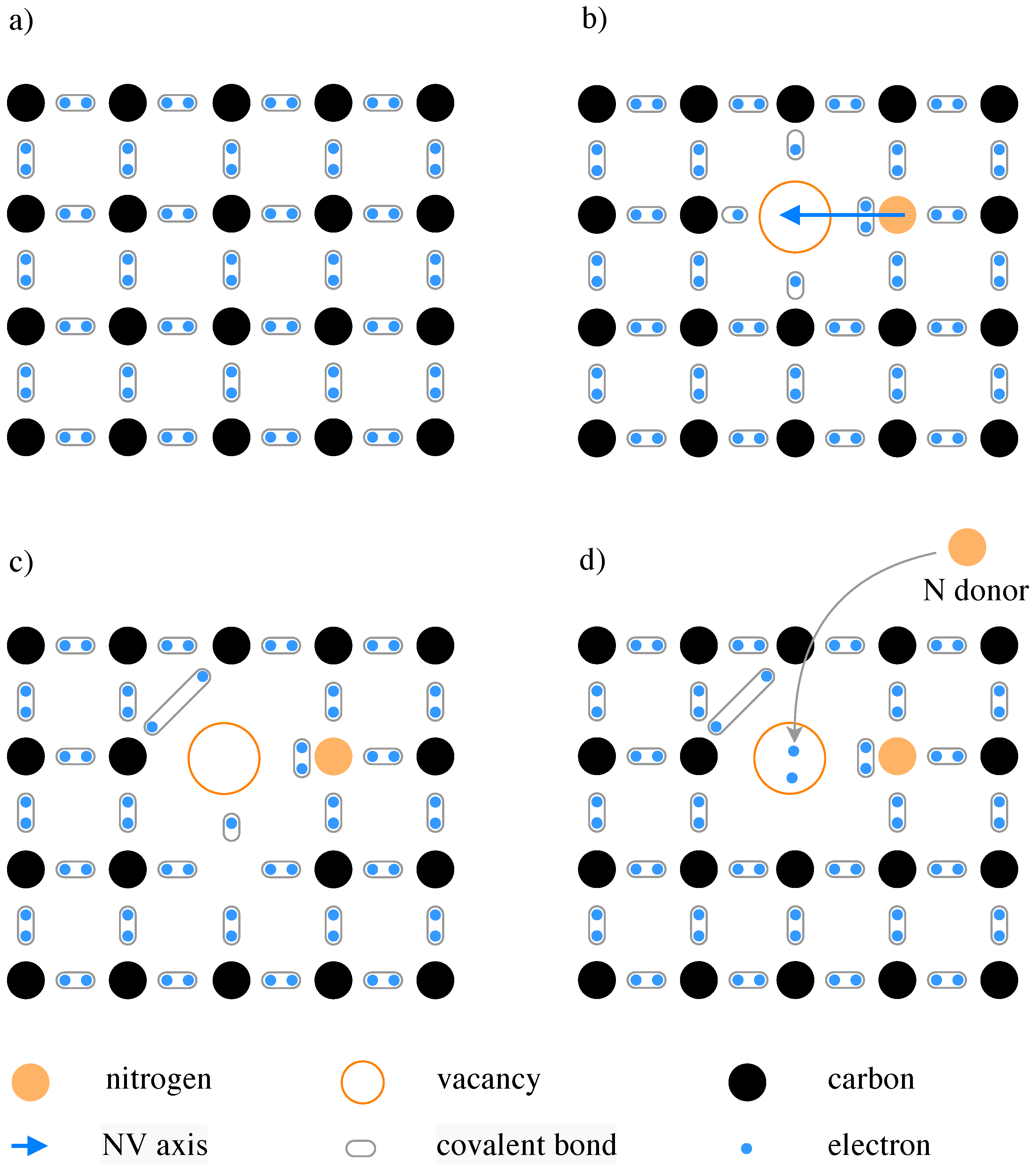
Figure 1. Simplified, flat representation of the diamond lattice. (a) A missing carbon atom, or vacancy, and the nearest neighbor, a substitutional nitrogen atom, create the N V center where the axis aligns the nitrogen atom with the vacancy, in one of four possible orientations. (b) The nitrogen atom has five electrons in the valence band, three of them form three covalent bonds with the three neighbor carbon atoms, leaving a lone pair. From the carbon atoms surrounding the vacancy, three electrons from dangling bonds are also part of the center, one remains unpaired, and the other two form a covalent bond (c). A total of five electrons leads to the neutral N V 0 state which does not exhibit the magnetic activity as the negative charge state N V does. When the center captures a sixth electron [22], normally from another nitrogen atom donor in the lattice (d), the center is charged negatively and shows the expected behavior useful in magnetometry.
Carbon 09 00016 g001
Figure 2. Energy levels scheme of a N V center. (a) Ground and excited states are split by spin interaction into a triplet. The electron is a fermion, its spin quantum number has a magnitude of s = 1 / 2 and two possible magnetic component m s = ± 1 / 2 . The two electrons in the N V center exist in a triplet state: one state where electrons have opposite spins ( m s = 0 ), and two degenerated states with electrons spin pointing to the same direction ( m s = ± 1 ) and higher energy. (b) The excitation (green arrows) conserves the spin and also the decay from m s = 0 excited to m s = 0 ground, however, when the center state is m s = ± 1 excited, one of the electrons flips and the state changes to m s = 0 , and the decay follows (preferentially) a non radiative path through the metastable singlet states, with the emission of a 639 nm (red arrow in the picture) photon corresponding to the zero phonon line (ZPL) and the decay from m s = ± 1 with the emission of a 1042 nm (infrared, black arrows in the picture), decreasing the observed PL intensity. The energy gap between m s = 0 and m s = ± 1 , in the ground and excited states, with zero field splitting, corresponds to 2.87 GHz and 1.42 GHz respectively.
Carbon 09 00016 g002
Figure 3. Experimental setup used for the characterization of the samples. It includes a 488 nm laser source, a piezo-positioner, a microscope objective lens, a dichroic mirror (94:06), a 488 nm notch filter, a beam splitter (90:10) a CCD camera, a spectrometer and other optical elements as shown in the diagram. The laser power source is 40 μ W which is partially absorbed by the dichroic mirror and the splitter, reducing the power incident on the sample to 11.25 μ W. The white LED is used for lighting and navigating the sample.
Carbon 09 00016 g003
Figure 4. Four views of the experimental setup at different levels of detail. Upper left: experimental setup including the teslameter probe (blue), electromagnet (left), objective (down), XYZ positioner (up) and resonator with diamond (center); Upper right: details of the electromagnet, the teslameter probe and the resonator with the diamond; Lower right: the resonator silver printed on the PCB with a diamond in the middle; Lower left: a zoom image of the single crystal diamond sample.
Carbon 09 00016 g004
Figure 5. Schema of a top view and a cross section of the resonator (a). The flat ring resonator is made up of a radiating patch, a dielectric substrate, and a grounding plate (b). The radiating ring structure was printed with silver on a substrate 1.3 mm PCB flat laminated composite substrate, made from a non-conductive material, and the grounding plate, a 0.08 mm thick copper foild. The geometric dimensions ( mm ) of the resonator are: L a = 16 , L b = 2.1 , W l = 0.5 W s = 0.5 , G = 0.2 , P w = 10.2 mm and P l = 30 mm . The inner and outer radius of the ring are: R i = 1.3 mm and R e = 3.7 mm respectively. S 11 is the resonator reflection coefficient (c), it is a ratio and therefore, a non-dimensional parameter but usually the magnitude is specified in dB ( 20 l o g | S 11 | ), for instance 0 dB indicates a magnitude | S 11 | = 1 which means that all the radiation applied is reflected and it is the case for this specific resonator at all frequencies different to the 2.87 Gz. The phase in red and the magnitude in blue show the response as designed.
Carbon 09 00016 g005
Figure 6. (a) Experimental measurement setup used to study the effect of the microwaves on the observed PL. The setup is simplified, the confocal microscope and other elements are replaced by the spectrometer and a Raspberry computer running a Python code to process and visualize the results. The microwave source and the resonator remain the same. (b) Experimental and simplified setup adding an electromagnet and using a photodiode (AMS TSL257-LF Amplified Si PD) and a Portenta H7 Arduino board instead of the spectrometer and the Raspberry. The microwave source, the resonator, laser, and optical elements remain the same.
Carbon 09 00016 g006
Figure 7. Observed dip for a bulk sample in the direction of the magnetic field in the crystallographic direction (other directions are also present but not represented in this case) of the photoluminescence at the resonance frequency (a) and split of the degenerated state because of the Zeeman effect (b).
Carbon 09 00016 g007
Figure 8. Zeeman splitting of the degenerated state under the effect of an external magnetic field B and experimental results (blue dots), observed for a bulk sample in the direction of the magnetic field in the crystallographic direction (other directions are also represented in Figure 9 and Figure 10). The energy splitting of the states m s = + 1 and m s = 1 (green and red lines) is 2 γ e B , linear and proportional to B with 2 γ the gyromagnetic ratio of the N V center. The zero splitting happens at the resonance frequency of 2.87 GHz . When the magnetic field reaches 0.1 T for the ground state and 0.05 T for the excited state, and then, due to the ground or excited state level anticrossing, the m s = 0 and m s = 1 states become equal in energy.
Carbon 09 00016 g008
Figure 9. Experimental measurement of photoluminescence as a function of the magnetic field for frequencies in the range of 2.7 to 3 GHz where it is observed how the gap between the resonance holes grows when the magnetic field increases. (a) is obtained by using the described electromagnet, changing the voltage and (b) is the result of the characterization moving the permanent magnet away at each step.
Carbon 09 00016 g009
Figure 10. Experimental measurement of photoluminescence as a function of the magnetic field for frequencies in the range of 2.7 to 3 GHz where it is observed how the gap between the resonance holes grows when the magnetic field increases. A 3D view, combining the three dimensions, photoluminescence, frequency, and magnetic field. (a) is obtained by using the described electromagnet, changing the voltage and (b) is the result of the characterization moving the permanent magnet away at each step.
Carbon 09 00016 g010
Disclaimer/Publisher’s Note: The statements, opinions and data contained in all publications are solely those of the individual author(s) and contributor(s) and not of MDPI and/or the editor(s). MDPI and/or the editor(s) disclaim responsibility for any injury to people or property resulting from any ideas, methods, instructions or products referred to in the content.