Article

Perovskite Solar Cell Efficiency and Thermal-Stability Enhancement via Interfacial Engineering: A Numerical Analysis


1
Department of Electrical Engineering, College of Engineering and Information Technology, Onaizah Colleges, Qassim 56447, Saudi Arabia
2
College of Engineering and Technology, American University of the Middle East, Egaila 54200, Kuwait
3
Electrical Engineering Department, Kafrelsheikh University, Kafrelsheikh 33511, Egypt
*
Author to whom correspondence should be addressed.
Inorganics 2026, 14(8), 196; https://doi.org/10.3390/inorganics14080196
Submission received: 1 June 2026 / Revised: 25 June 2026 / Accepted: 22 July 2026 / Published: 24 July 2026

Abstract

The marketable viability of perovskite solar cells (PSCs) is currently hindered by challenges related to interfacial charge-carrier extraction and thermal degradation. This study presents a comprehensive finite element method (FEM) analysis using COMSOL Multiphysics to evaluate the efficacy of bi-layer electron transport layer (ETL) engineering in addressing these limitations. We developed a coupled optical–electrical model to investigate three planar architectures: a conventional TiO2-based reference device, a TiO 2 / SnO 2 bi-layer configuration, and a TiO 2 / SnO 2 : Fe (iron-doped) bi-layer device. Simulation results under AM1.5G illumination reveal that the bi-layer configurations significantly enhance optical absorption across the visible spectrum (350–700 nm) compared to the single-layer counterpart. The incorporation of Fe-doped SnO2 resulted in optimized energy band alignment, creating a favourable conduction band offset that facilitates electron extraction. Consequently, the TiO 2 / SnO 2 : Fe device achieved a peak power conversion efficiency (PCE) of 18.3% at 300 K, outperforming the undoped bi-layer (18.0%) and the reference device (17.5%). Furthermore, thermal stress simulations indicated that the Fe-doped architecture exhibits superior stability, maintaining a PCE of 12.8% at 440 K compared to 12.3% for the reference. This enhanced performance is attributed to the passivation of interfacial defects and the formation of a stronger built-in electric field at the ETL/absorber junction, validating the strategic doping of metal oxides as a robust pathway for high-efficiency, thermally stable perovskite photovoltaics.

1. Introduction

The urgent demand for sustainable and renewable energy has stimulated research into the development of highly efficient and cost-effective photovoltaic (PV) technologies [1]. Recently, perovskite solar cells (PSCs) have arisen as one of the most promising candidates for upcoming photovoltaic generation, owing to their remarkable optoelectronic properties and low fabrication cost [2]. Since its first demonstration in 2009, the power conversion efficiency (PCE) of PSCs has risen from less than 4% to over 26%, this material has revolutionized the world of solar cells, making it a major competitor to monocrystalline silicon, which has been around for over a decade [3]. Until now these solar cells did not achieve what it takes to replace the traditional silicon (Si) solar cells due to two major challenges: interfacial charge transport and device stability [4]. The interfaces between the perovskite absorber and the adjacent charge transport layers are of paramount importance for evaluating photovoltaic performance and ensuring the long-term durability of the device [5]. Defects, mismatched energy levels, and interfacial recombination at these junctions often lead to a reduction in open-circuit voltage (Voc), fill factor (FF), and stability losses under operating conditions [4]. To solve these problems, it is recommended to develop robust, efficient, and well-aligned transport layers. Within the various components of PSCs, the electron transport layer (ETL) is particularly important because it ensures selective electron extraction, blocks holes, and reduces recombination, thereby contributing to the efficiency and stability of perovskite cells [6].
Traditionally, titanium dioxide (TiO2) has been widely adopted as an ETL due to its suitable band alignment, chemical stability, and simple fabrication methods [7]. However, TiO2 has certain limitations, such as low electron mobility, high processing temperature (>450 °C), UV degradation, and hysteresis effects, which restrict its compatibility with flexible substrates and long-term performance [8].
To overcome these drawbacks, tin dioxide (SnO2) has attracted considerable interest as a perfect alternative to ETL [9]. It has superior electron mobility, higher optical transparency, a wider band gap, and can be processed at much lower temperatures than TiO2 [9]. In addition, it has improved stability under UV illumination and has enabled PSCs with efficiencies greater than 23% to be achieved in several studies [10]. Nevertheless, intrinsic defects, surface traps, and imperfect energy band alignment can still impair device performance, motivating further modification of SnO2-based ETL compositions [10].
Numerous dopants, containing Mg, Nb, Ta, and Li, have been examined to enhance the electrical and interfacial assets of SnO2-based ETL. Several approaches have been made to optimize SnO2 one of these involves doping this layer with metal ions, which makes it possible to adjust the carrier concentration, reduce recombination centres, and improve band alignment with the perovskite layer [11]. Doping with transition metals has been shown to passivate defects and improve interfacial properties [12]. Among these metals, iron has been proposed as a candidate promoter to improve electron extraction and completely reduce the rate of interfacial recombination due to its ability to modify the electronic structure of SnO2, modify carrier transport features.
The study elaborated by [13] shows that electronic interaction between iron and the SnO2 crystal lattice is possible, which influences electron transport in ETL. In summary, the ETL plays a crucial role in the performance and stability of perovskite solar cells [14,15]. While TiO2 remains a standard ETL, its limitations in terms of mobility, UV stability, and interfacial recombination are motivating researchers to develop a bi-layer ETL to achieve better performance [16,17]. A good candidate to fulfil this objective could be the SnO2 and iron-doped SnO2 that offer promising prospects for improving charge extraction, reducing recombination, and enhancing optical absorption.
In spite of the rapid enhancement of recently fabricated PSCs, still the long-term operating stability, large-scale industrial production, lead toxicity, environmental degradation, encapsulation requirements and marketable positioning remain substantially associated with established crystalline silicon solar cells. But, their low-temperature handling, tunable optoelectronic features, and low-cost production push research toward future marketable production. Recent studies presents materials for PSCs which are chemically stable and have tunable electronic properties that enable highly efficient and stable devices [18].
The main aim of this work is to establish an adequate interpretation and analysis of the usage of iron-doped SnO2 in ETL. To do this, a finite element model will be developed in COMSOL Multiphysics (5.3). This model aims to explore three different ETL structure topologies: (i) a reference composition that is formed from TiO2 alone, (ii) a second structure that is composed from bi-layer TiO2/SnO2, (iii) and, finally, a third configuration that contains TiO2 and iron-doped SnO2. Different simulation scenarios will be adopted that allow us to correlate structural, optical, and electronic properties with device performance and stability.
The other parts of this work are arranged as follows: Section 2 illustrates the proposed PSC structures. The simulation results of the proposed PSCs are presented in Section 3. Finally, Section 4 accomplishes the main deductions.

2. Results and Discussions

2.1. COMSOL Simulation

The ETL thicknesses and doping conditions in this study are not fixed; they were variable in the study and the PCE for each device was calculated and mathematically analyzed.

2.1.1. Band Diagrams

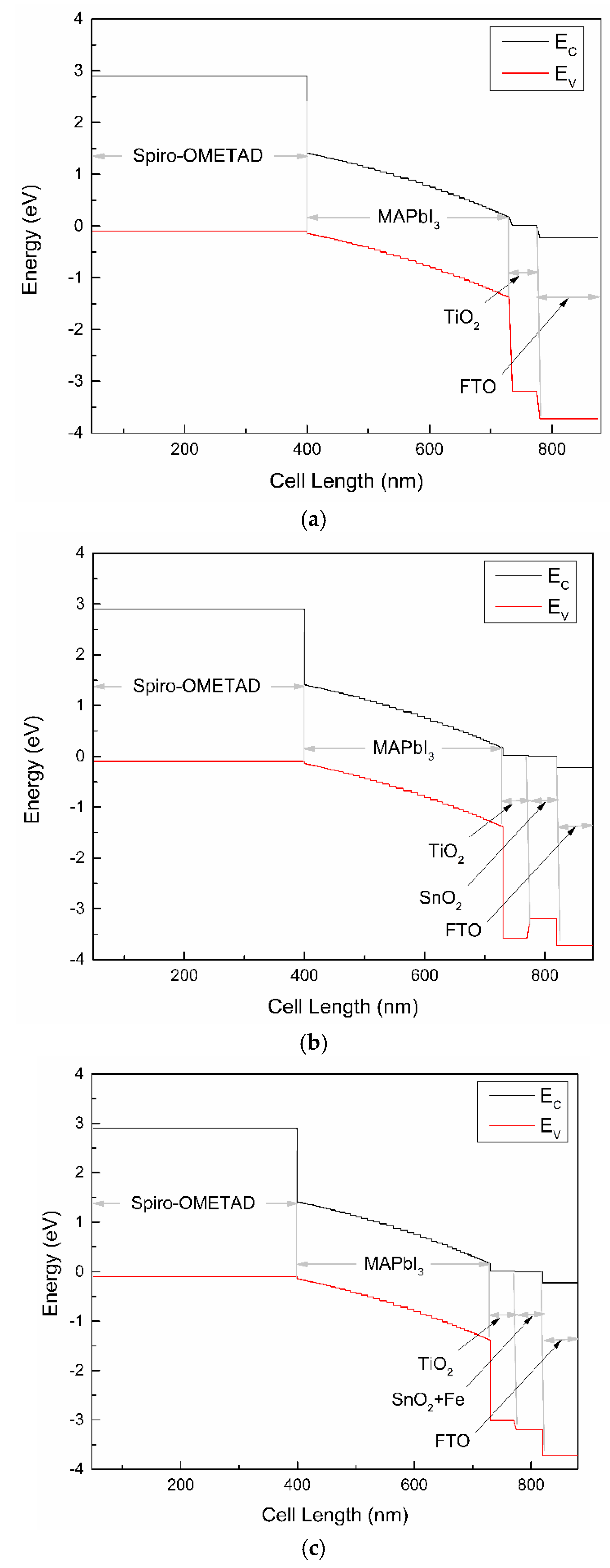
Figure 1 shows the COMSOL-simulated band diagrams for three semiconductor devices: a reference structure, Device 1, and Device 2. Each diagram depicts the spatial distribution of the conduction band edge (EC) and valence band edge (EV) as a function of cell length (nanometres). These profiles are critical for understanding the electrical characteristics, carrier transport behaviour, and possible obstacles in each device design. The energy band alignment influences the flow of charge carriers (electrons and holes), which affects recombination kinetics, built-in electric fields, and overall device efficiency.
The reference structure (Figure 1a) exhibits a unique energy band arrangement, with the conduction band (EC) at around 3 eV at the surface and gradually decreasing throughout the device length. Similarly, the valence band (EV) begins at 0 eV and gradually decreases, suggesting a potential gradient throughout the device. The step-like discontinuities at specified points (~400 nm and ~800 nm) represent heterojunction interfaces or material transitions. The energy band alignment implies a built-in electric field that directs electron flow into lower potential areas, improving carrier separation and reducing recombination losses.
Device 1 (Figure 1b) has a somewhat different conduction and valence band profile than the reference. The conduction band has a smoother potential drop, but the valence band has small abnormalities in the interface areas. These variances imply minor differences in doping concentration, interface quality, or material composition. The smoother conduction band may boost electron transport by lowering scattering barriers, resulting in increased mobility. However, tiny changes in the valence band might trap holes locally, thereby enhancing recombination.
Device 2 (Figure 1c) demonstrates an additional evolution of the band profile, notably with more prominent steps in both EC and EV at the device’s conclusion. This phenomenon might be caused by extra layers or more abrupt heterojunctions. The prolonged slope of both bands suggests a larger built-in electric field, which improves carrier separation and drift. However, abrupt transitions may produce localized states or tunnelling sites that affect charge recombination and transport dynamics. The lower final valence band energy indicates increased hole extraction capacity, which is useful for devices such as solar cells and photodetectors.
The three devices show a definite development in energy band engineering. The reference structure establishes a baseline with well-defined potential barriers and mild electric fields. By introducing a SnO2 intermediate layer in Device 1, a more harmonious alignment of the conduction bands is achieved, which simplifies electron extraction and decreases interfacial recombination. By adding doped SnO2 to Fe in Device 2, the curvature of the bands can be optimized, which promotes efficient charge transfer. The results demonstrate that bi-layer and doped ETL configurations significantly improve electronic properties compared to the single-layer TiO2 reference. More precisely, the shift of the valence band significantly influences the performance of the device, as it determines the transport of holes to the HTL, while the shift of the conduction band has an impact on the electron injection in the ETL.

2.1.2. Optical Properties: Absorption and EQE

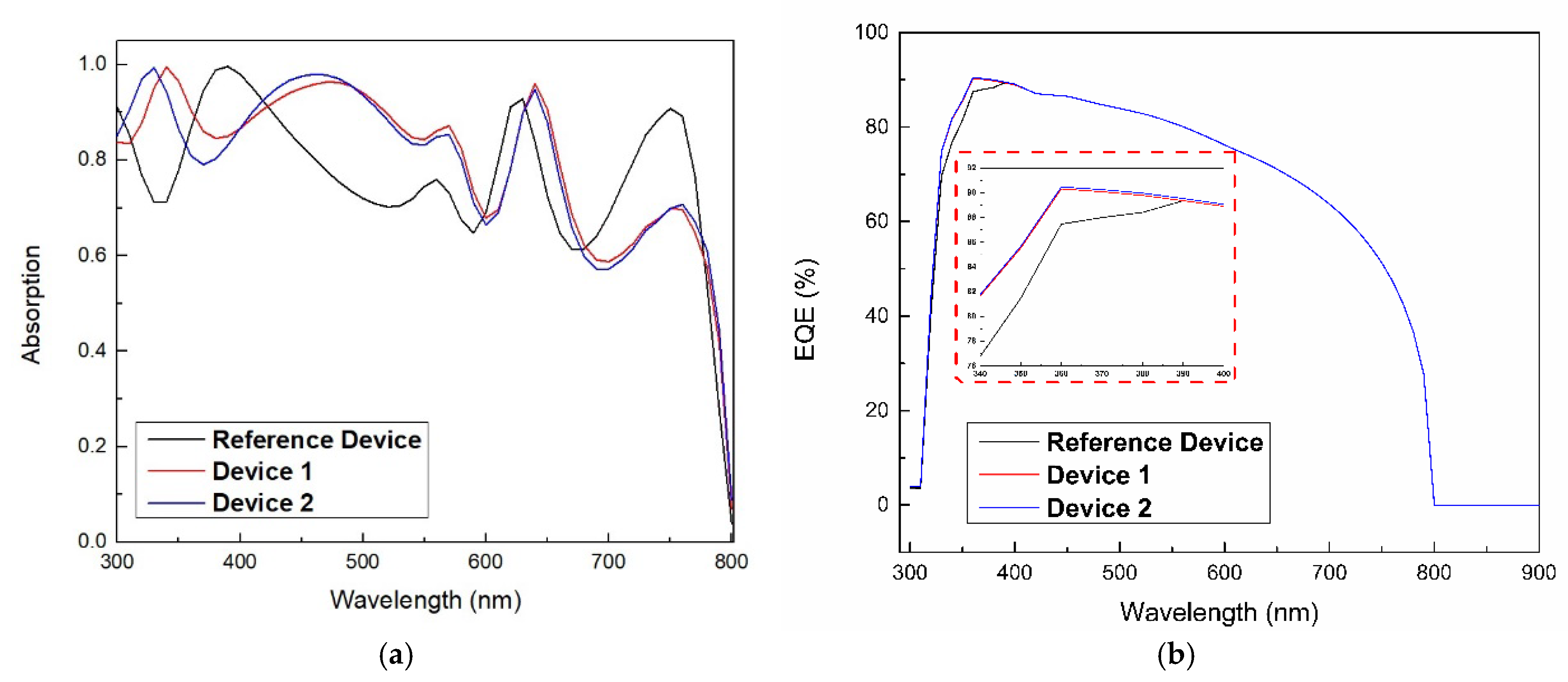
The optical properties of these three devices are presented in Figure 2. On the left, we compare the simulated absorption of the reference device (ETL TiO2) with that of Device 1 (double-layer TiO2/SnO2) and Device 2 (double-layer TiO2/iron-doped SnO2). The two bi-layer ETLs have a stronger and more regular absorption over most of the visible spectrum (350–700 nm) compared to the single-layer TiO2 reference, which corresponds to an improved optical coupling and a reduction in parasitic losses at the front interface.
Device 1 exhibits slightly higher absorption in the short wavelength region compared to Device 2, which may reflect a slight change in refractive index or absorption induced by iron doping; however, both double-layer designs offer nearly identical performance in longer wavelengths. The improvement in absorption in double-layer devices should increase photoelectric current production and, combined with better band alignment, increase photovoltaic efficiency. The quantum efficiency of the cells for these three devices is illustrated in Figure 2b, confirming this improvement. Based on these graphs, it can be said that Device 2 performs better than Device 1 in a spectral range between 350 and 450 nm. This can be attributed to the doping of SnO2 with Fe compared to undoped SnO2. As a result, Device 2 can improve more electron extraction from the ETL to the back contact. The integrated optical quantities for investigated devices are shown in Table 1.

2.1.3. Electrical Output: JV and Power Curves

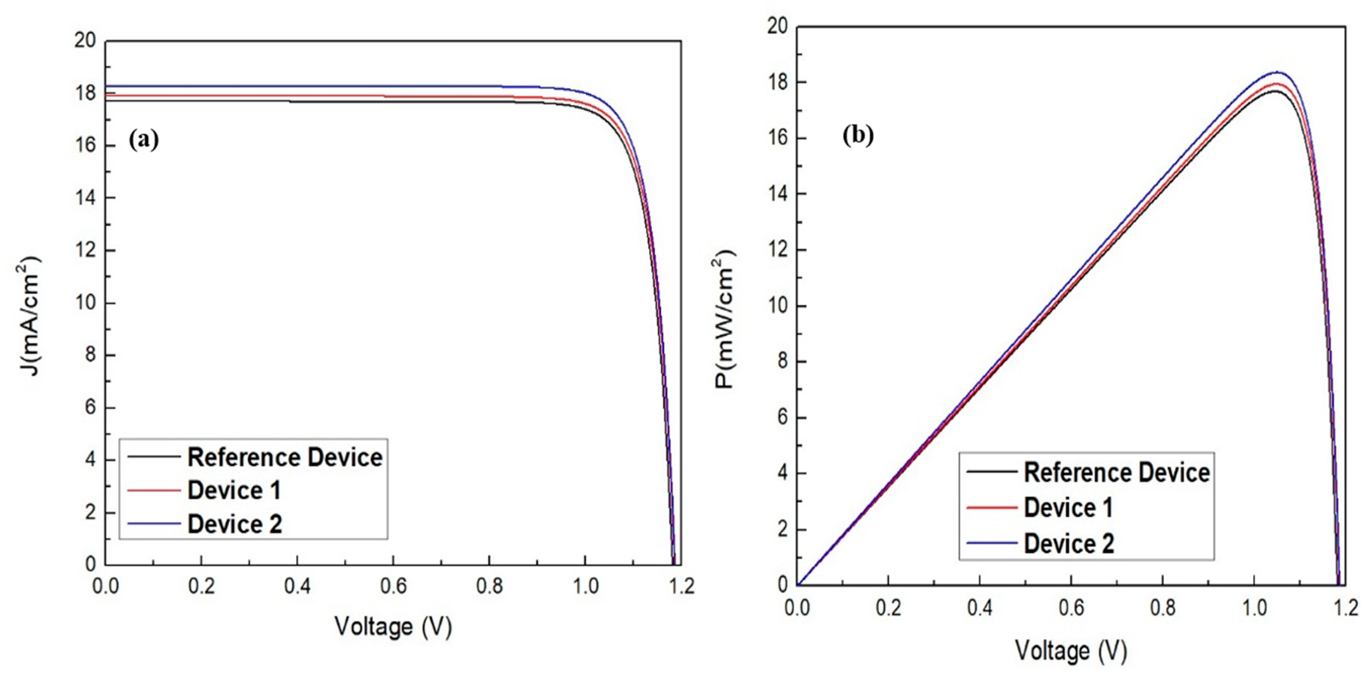
Figure 3a,b show the J-V curves (current density J vs. applied voltage V) and PV curves (power density P vs. applied voltage V) of three devices: reference (black), Device 1 (red), and Device 2 (blue). The J-V graphs show current density (mA/cm2) vs. applied voltage (V) ranging from 0 to 1.2 V. All three devices have a similar short-circuit current density (Jsc) of around 17.8 to 18.1 mA/cm2 when V = 0. The curves stay flat at low-to-moderate voltages, demonstrating minimal series resistance and steady photo-generated current. Near the open-circuit area (≈between 1.1 and 1.2 V), the current drops sharply to zero, indicating Voc values between 1.16 and 1.18 V. Device 2 (blue) has the greatest Jsc and slightly greater Voc, whereas Device 1 (red) is marginally lower than the reference device (black). The nearly equal Jsc values show that all devices absorb light and generate charge similarly.
Slight improvements in Device 2 indicate a little improvement in either absorption, carrier collection, or decreased recombination. Voc changes are modest (~10 s of mV). The slightly greater Voc for Device 2 might suggest less recombination or somewhat better energetic alignment. Furthermore, the almost flat part of the J-V curves and the identical slopes up to mid-voltages indicate low series resistance and equivalent shunt characteristics. There are no noticeable roll-over or substantial asymmetries, which would imply high parasitic resistance.
In terms of PV characteristics, all devices progress linearly from 0 V to the maximum power point (MPP) between 1.02 and 1.08 V before dropping to zero at a Voc of 1.16 to 1.18 V. The peak power densities are approximately: reference ≈ 17.95 mW/cm2, Device 1 = 17.70 mW/cm2, and Device 2 ≈ 18.25. The peaks occur at voltages somewhat lower than Voc, as predicted. As demonstrated in Figure 3b, Device 2 has the highest Pmax, followed by the reference and Device 1. This order reflects the minor variances in Jsc and Voc. The gains reported in Device 2 (higher Jsc and Voc) are consistent with minor enhancements in optical absorption or recombination suppression.
Convergence analysis has been performed by systematically refining the simulation mesh density. The results confirm that the calculated PCE values are stable within a deviation of less than 0.05%, demonstrating numerical reliability as presented in Table 2.
Although the total efficacies attained in this work stay under the present state-of-the-art investigational PSCs archives (>26%), the determination of the current examination is to enumerate the lonely influence of ETL manufacturing under precise imitation settings. The detected enhancements reveal that Fe-doped SnO2 can offer improvements in carrier pulling out and thermal robustness, creating a hopeful constituent for incorporation into future high-efficiency PSC constructions.

2.1.4. Effect of Temperature

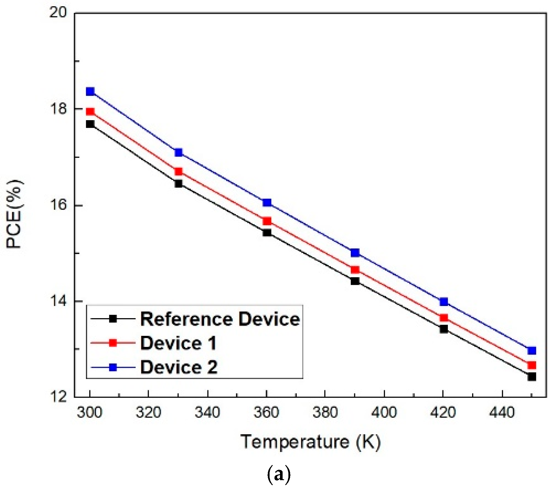
Figure 4a shows the fluctuation in power conversion efficiency (PCE) degradation as a function of temperature for three different designs of perovskite solar cells: the reference device, Device 1, and Device 2. It is well known that photovoltaic performance is significantly dependent on operating temperature, which is crucial for the stability and effectiveness of the device in practical applications. All devices show a monotonic drop in PCE with rising temperature across the examined temperature range of 300–450 K. The overall thermal instability of perovskite solar cells, where higher temperatures raise non-radiative losses, decrease charge transport efficiency, and speed up carrier recombination, is consistent with this tendency.
For precision, the main photovoltaic, electric field, recombination, and thermal-stability metrics of all the examined devices are presented in Table 3. This assessment highpoints the profits of bi-layer ETL manufacturing and the effect of Fe integration on complete device performance.
Device 2 obtains the greatest PCE (~18.3%) at room temperature (300 K), followed by Device 1 (~18.0%) and the reference device (~17.5%). The PCE values decrease to around 13% for Device 2, 12.7% for Device 1, and 12.3% for the reference device when the temperature rises to 440 K. Device 1 and 2 continuously exceed the reference device despite the general deterioration trend, demonstrating the usefulness of interface engineering by including SnO2 and SnO2 + Fe.
Furthermore, at all temperatures, the reference device has the lowest PCE. This is because the electron transport layer (ETL) is only TiO2, which has drawbacks including comparatively poor electron mobility and possible hysteresis effects. Higher interfacial recombination losses occur when there is no additional passivation or charge-extraction layer present, especially at higher temperatures.
Because SnO2 has greater electron mobility and energy band alignment than TiO2, adding a layer of SnO2 to Device 1 increases electron extraction efficiency. This leads to decreased recombination and series resistance, which accounts for the steady improvement in PCE over the reference device. Because SnO2 can function as a protective layer, reducing interfacial deterioration, we should see that the thermal stability is also marginally improved. Across the whole temperature range, Device 2 has the greatest PCE. Fe doping in the SnO2 ETL, which is known to promote band alignment, passivate trap states, and electrical conductivity, is responsible for this. Amongst the examined constructions, the TiO2/SnO2:Fe formation improves electron extraction, which results in a more resilient device under heat stress, this configuration demonstrated the maximum imitation routine metrics and enhanced thermal stability under the approved modelling circumstances [19]. The efficacy of interface modification techniques is therefore demonstrated by Device 2, which exhibits the most promising thermal resilience and efficiency.
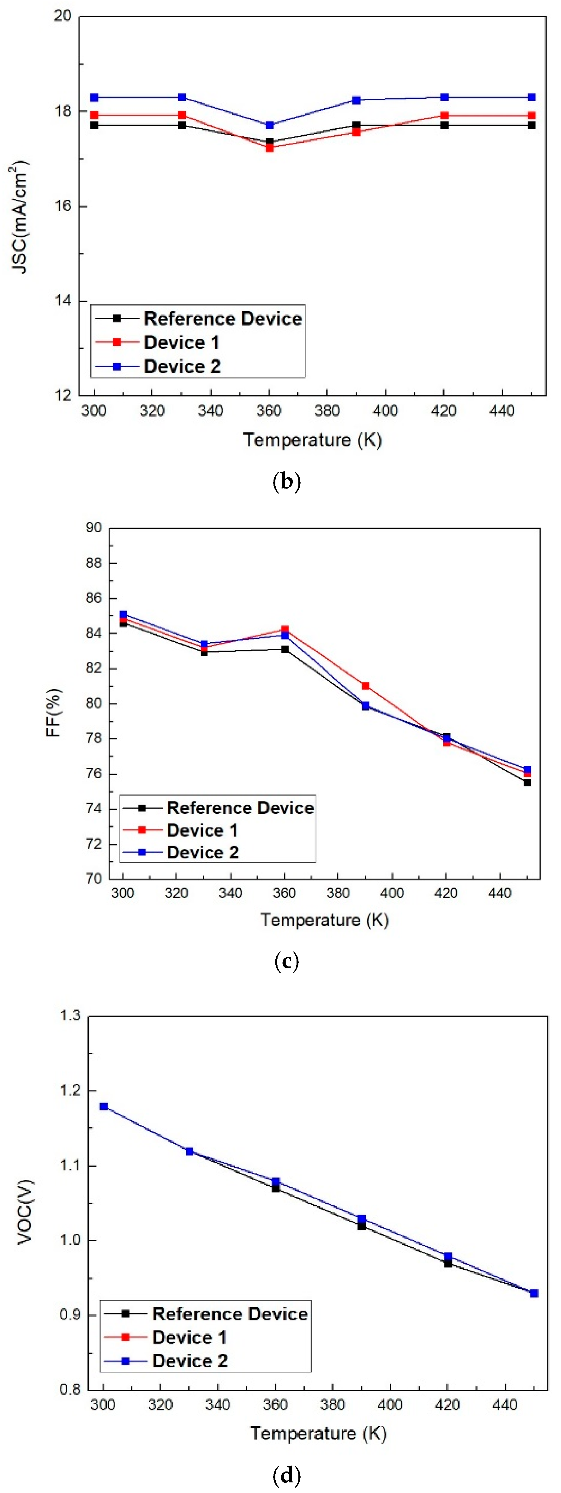
On the other hand, all devices’ short-circuit current density (JSC) fluctuates somewhat with temperature, staying between 17 and 18.5 mA/cm2 (Figure 4b). Device 1 and the reference device are the next two devices that consistently display the highest JSC, after Device 2. A balance between enhanced recombination and bandgap narrowing is indicated by the slight drop seen at 360 K. Raising the temperature concurrently increases ion migration and non-radiative recombination, which restrict the efficiency of carrier extraction, while decreasing the perovskite bandgap, which permits more photon absorption. Fe doping in SnO2, which passivates interfacial trap states, improves electron transport, and lowers recombination losses, is responsible for Device 2’s higher JSC. This demonstrates how ETL adjustment improves interface quality and carrier extraction.
As anticipated, the fill factor (FF) shows thermal deterioration in device function, dropping from around 84–85% at 300 K to roughly 76% at 450 K (Figure 4c). The main causes of this decrease are decreased shunt resistance and increased series resistance. Heat-activated trap states lead to increased non-radiative recombination. Interfacial deterioration and hysteresis are caused by ion migration effects. The FF trends of all three devices are comparable, indicating that resistance and bulk recombination effects outweigh variations caused by ETL. Nonetheless, the effect of enhanced ETL quality and decreased recombination is confirmed by Device 1 and 2’s somewhat greater FF around mid-temperature points.
As seen in Figure 4d, this simulation study is accomplished by evaluating the impact of temperature on the open-circuit voltage (VOC) for the three devices. It is noteworthy that for all devices VOC drops almost linearly as temperature rises. Device 1 is in the middle of Device 2 and the reference, whereas Device 2 retains the highest VOC levels. The observed results for high-quality perovskite solar cells are consistent with the average slope of −1.7 mV/K.
Increasing temperature causes a significant rise in J0 (the reverse saturation current). The decrease in VOC is dominated by the rise in J0 and increased recombination since JSC stays almost constant. Because Device 2 has a stronger passivated interface and greater electron extraction through SnO2 + Fe, it performs better due to its lower J0.
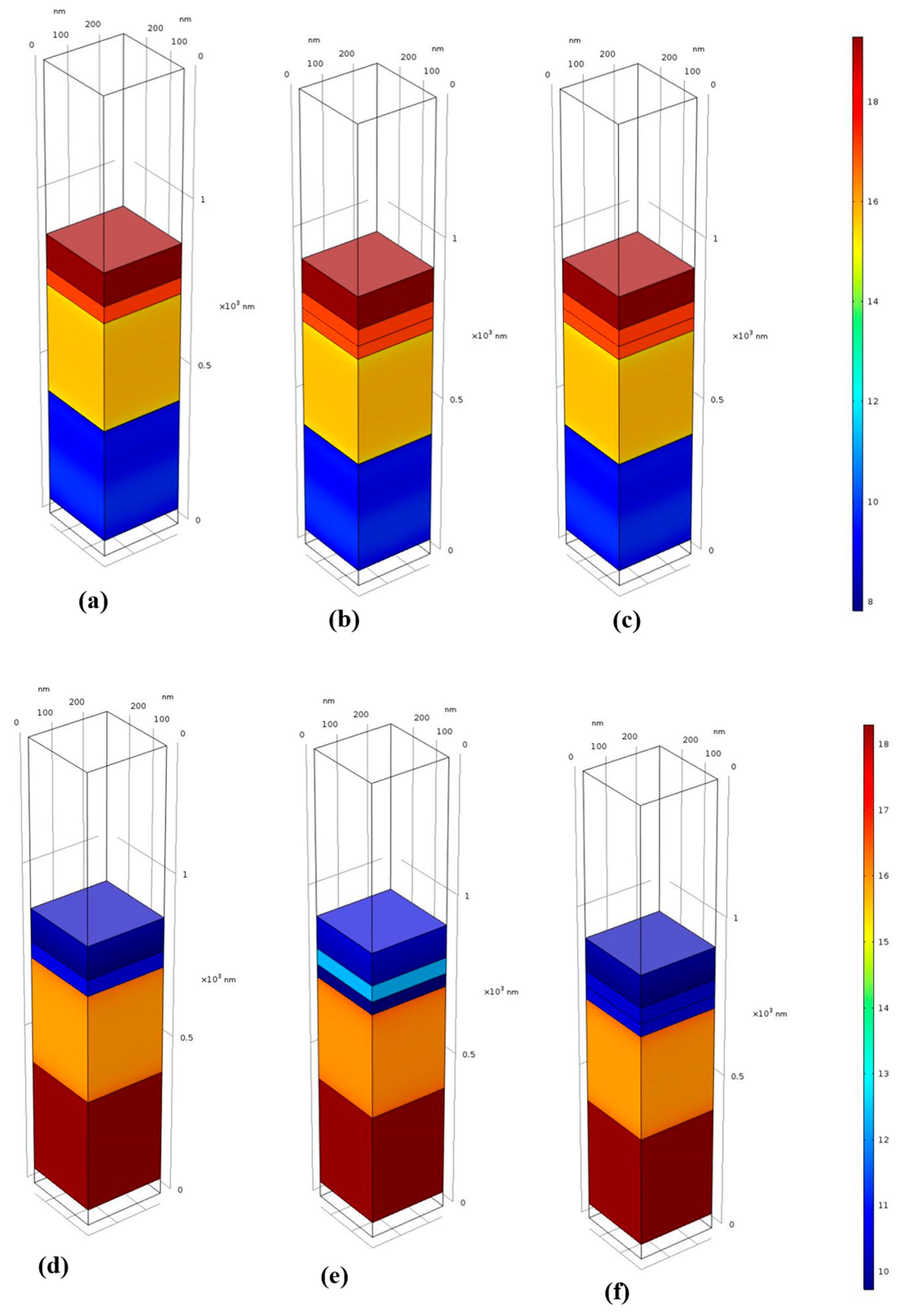
The electron and hole densities, illustrated in Figure 5 for the three devices, clearly demonstrate the effect of temperature change on the devices. This influence is evident across the different layers of the photovoltaic cell (PSC), after applying the decimal logarithm to better illustrate the amplitude of the variations in charge-carrier concentrations.
Figure 5 confirms the expected behaviour: the electron density gradually decreases from its maximum value at the FTO contact to its minimum value at the base of the HTL. Conversely, the hole density is highest at the bottom of the HTL and lowest near the FTO contact. The temperature variation has a moderate effect on carrier concentration, but it has a greater impact on electron density than on hole density. This effect can be explained by the fact that temperature significantly influences the density of minority carriers (in this case, electrons in a p-type absorber) rather than that of majority carriers. While the recommended TiO2/SnO2:Fe bi-layer ETL proves enhanced photovoltaic steadiness at raised temperatures, the present simulation outline does not clearly model degradation paths such as ion migration, material decay, or interfacial chemical degradation. Consequently, the attained outcomes should be understood as pointers of improved thermal working performance rather than comprehensive long-term thermal dependability.
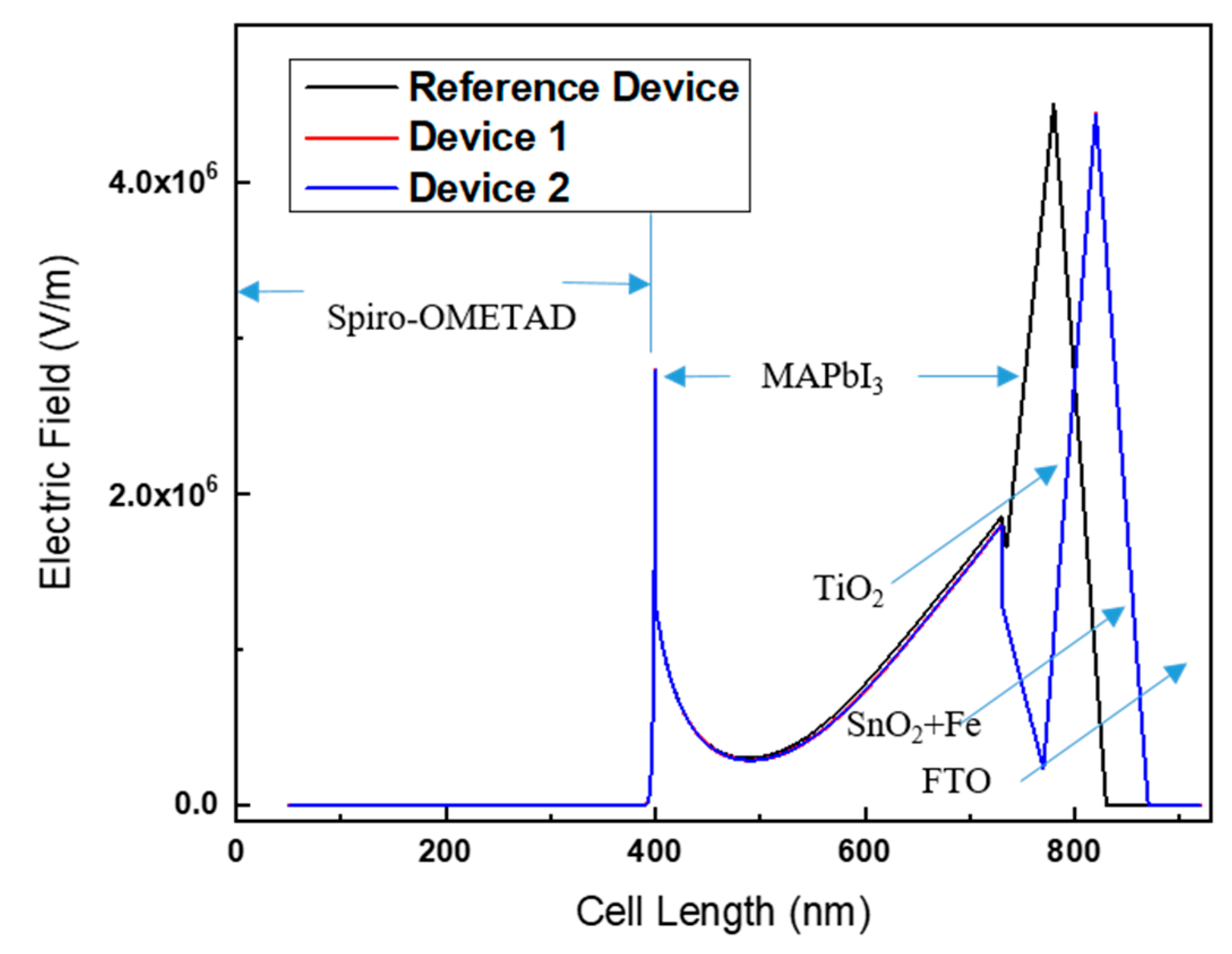
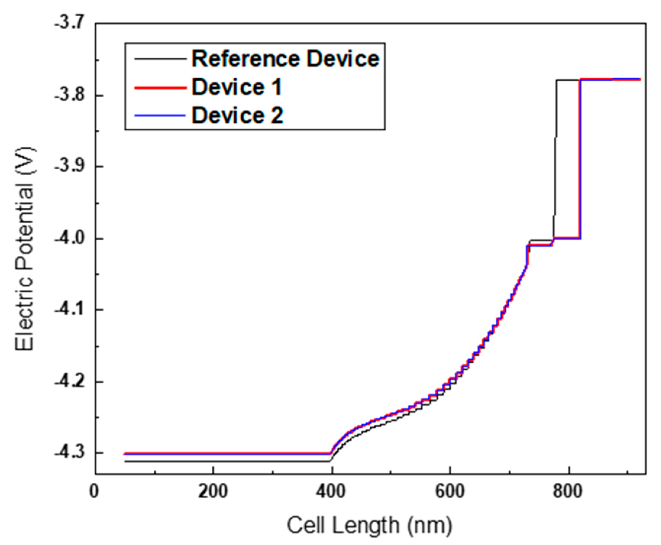
The spatial distributions of the internal electric field and electrostatic potential that elucidate the charge separation and transport mechanisms within the investigated perovskite solar cell architectures are shown in Figure 6 and Figure 7. Across all devices, the electric field is primarily concentrated at the heterointerfaces, while remaining relatively weak within the bulk of the MAPbI3 absorber, confirming that carrier transport is largely governed by interfacial band bending rather than bulk depletion. In the reference device (FTO/TiO2/MAPbI3/Spiro-OMeTAD/Ag), a pronounced electric field peak reaching approximately (4–4.5) × 106 V m−1 is observed near the perovskite/HTL interface, while a weaker field (~1–2 × 10⁶ V m−1) appears at the ETL/absorber junction. This asymmetric field distribution arises from the modest conduction band minimum (CBM) mismatch between TiO2 (χ ≈ 4.0 eV) and MAPbI3 (χ ≈ 3.93 eV), which forms a shallow cliff that promotes electron accumulation at the interface, partially screening the built-in potential. This effect is further confirmed by the electrostatic potential profile, which shows a reduced potential drop across the ETL/MAPbI3 junction and a smoother potential gradient within the absorber, indicative of limited driving force for carrier extraction. Upon insertion of an SnO2 inter-layer (Device 1: FTO/TiO2/SnO2/MAPbI3/Spiro-OMeTAD/Ag), the electric field within the absorber becomes more uniformly distributed, with a moderate enhancement near the ETL interface and a peak magnitude of approximately 3.5–4 × 10⁶ V m−1. This improvement is attributed to the significantly higher electron mobility of SnO2n ≈ 100 cm2 V−1 s−1) compared to TiO2n ≈ 20 cm2 V−1 s−1), which reduces electron accumulation and flattens the quasi-Fermi-level gradient. However, the potential profile reveals that the TiO2/SnO2 conduction band offset still introduces an internal energy discontinuity, limiting the maximum attainable built-in potential across the ETL/absorber interface.
In Device 2 (FTO/TiO2/SnO2:Fe/MAPbI3/Spiro-OMeTAD/Ag), a marked increase in the electric field strength is observed at the ETL/MAPbI3 junction, with peak values exceeding 4.5 × 10⁶ V m−1, accompanied by a steeper potential drop localized at this interface. This behaviour originates from the Fe-induced adjustments of the ETL electronic construction and interfacial assets, which reinforce the built-in electric field and facilitate charge pulling out at the ETL/MAPbI3 boundary. The enhanced device routine is therefore accredited mainly to improve carrier transportation and reduced interfacial losses.
The resulting stronger interfacial electric field enhances the drift component of electron transport, facilitating faster carrier separation and extraction into the ETL while suppressing interfacial charge accumulation.
Overall, the combined electric field and potential analyses confirm that optimized band alignment at the ETL/absorber interface directly translates into a higher internal field, improved carrier collection efficiency, and superior photovoltaic operation, while excessive band discontinuities or charge accumulation reduce the effective built-in potential and weaken field-assisted transport.

3. Materials and Methods

3.1. Modelling and Structure

Using COMSOL Multiphysics software (5.3), the optical and electrical performance of PSC with the thin-film structure reported in the literature [20] is examined and evaluated. This paper focuses on the effect of adopting an ETL bi-layer (TiO2/SnO2) and studies the impact of doping SnO2 with Fe on the optical and electrical performance.
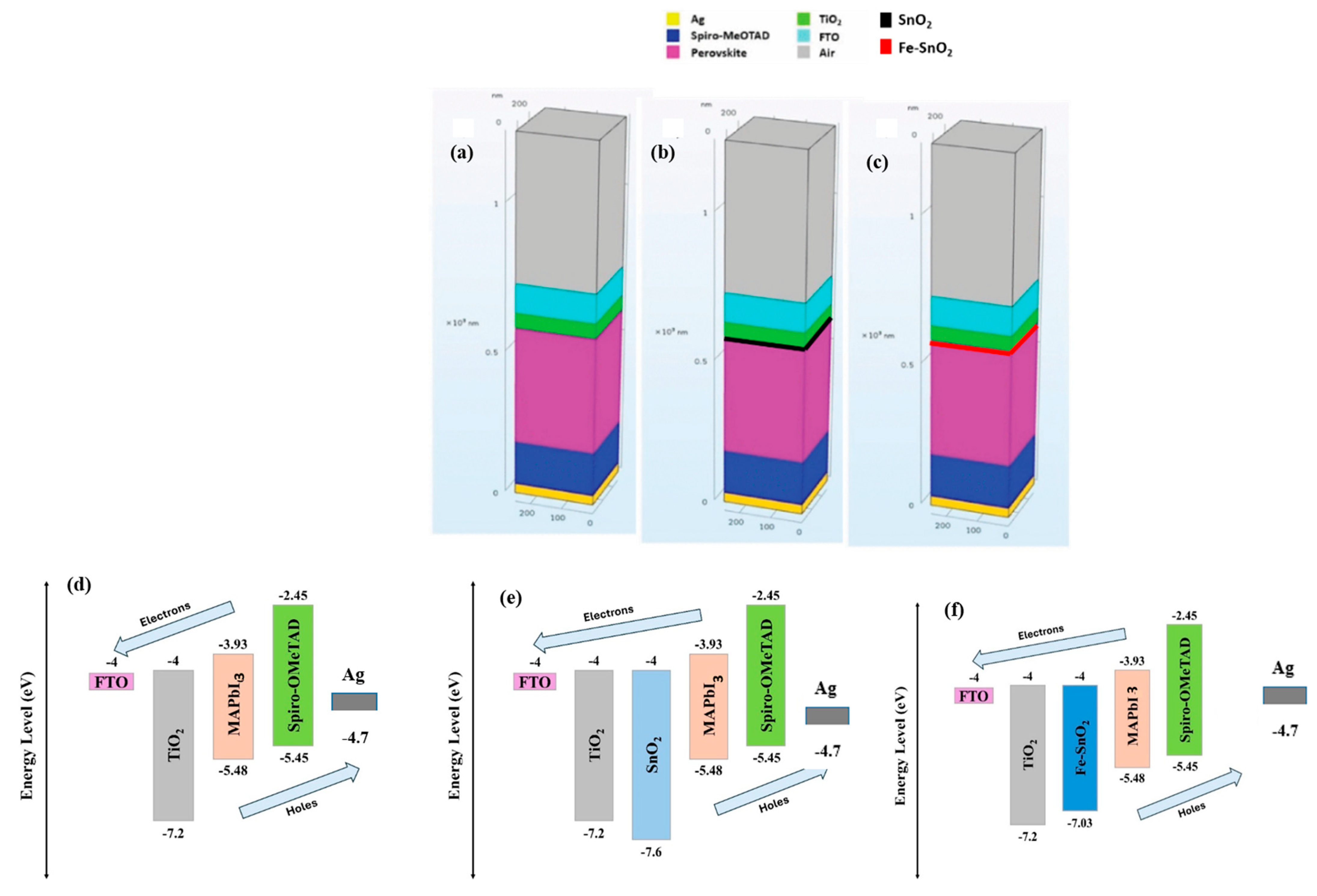
Figure 8 represents the reference device structure that is composed from (arranged from top to bottom) a fluorine-doped tin oxide (FTO): the electron transportation layer (ETL) is n-doped TiO2, the absorber layer is p-doped MAPbI3 perovskite, the hole transportation layer (HTL) is p-doped Spiro-OMeTAD, and the metallic contact layer is silver. An air layer was added to the cell surface to provide precise optical modelling. Figure 1 represents the proposed schematic of the three structures.
Figure 8a–c show the structures of the reference device and Device 1 and 2. Where Device 1 and 2 are approximately similar to the reference device and the only difference is exhibited at the ETL level. A bi-layer instead of a single-layer is considered: TiO2/SnO2 for Device 1 and a TiO2 with Fe-doped SnO2 for Device 2 (Table 4).

3.1.1. Geometry and Domain

The simulation domain was constructed based on an anticipated experimental planar structure: FTO/TiO2/SnO2 + Fe/MAPbI3/Spiro-OMETAD/Ag. Accurate geometrical definitions are crucial for calculating optical interference effects and electric field distribution. The layer thicknesses ( L ) , derived from the fabrication process, are detailed in Table 5, yielding a total simulated active layer stack thickness of 970   nm . The Ag layer thickness of 100   nm was included primarily for defining the electrical back contact.
While the charge-carrier transport is predominantly unidirectional, allowing for a 1D approximation in the electrical model, optical wave propagation requires the definition of a small unit cell to account for light incidence and reflection phenomena accurately. A 2 D geometry ( x y p l a n e ) was defined for the simulation, where the depth axis (x) corresponds to the transport direction, and a small lateral dimension ( L y = 500   nm ) was set. To model the incident sunlight and ensure rigorous electromagnetic boundary conditions, an air domain ( 1000   nm   t h i c k ) was placed above the FTO layer, terminated by a perfectly matched layer (PML) to absorb outgoing waves and prevent non-physical reflections (Figure 8).

3.1.2. Optical–Electrical Coupling

The optoelectronic model operates by solving the optical problem first under the standard AM1.5G illumination and then using the resulting photogeneration profile as the source term in the subsequent electrical drift-diffusion simulation. All optical and electrical properties of the specified materials were sourced from pertinent research [20,21,22,23] and employed for modelling either through the COMSOL material library or by hand incorporation into the construction.
Table 5 delineates the principal parameters of PSC, wherein εr represents the dielectric factor of the substance, Nc and Nv denote the effective concentration of states in the conduction and valence bands, respectively, μn and μp signify the mobilities of both electrons and holes, respectively, NA and ND indicate the doping densities of acceptor and donor atoms, respectively, and τn and τp refer to the lifetimes of electrons and holes, respectively.
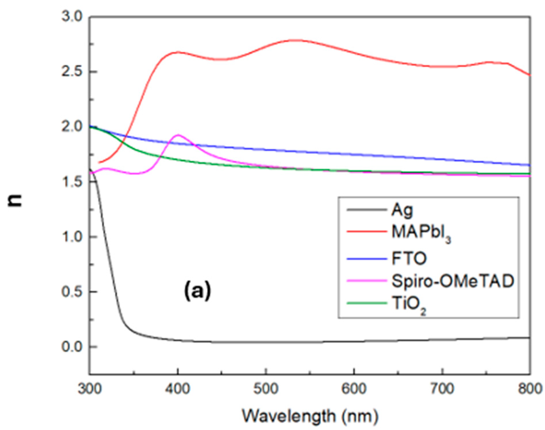
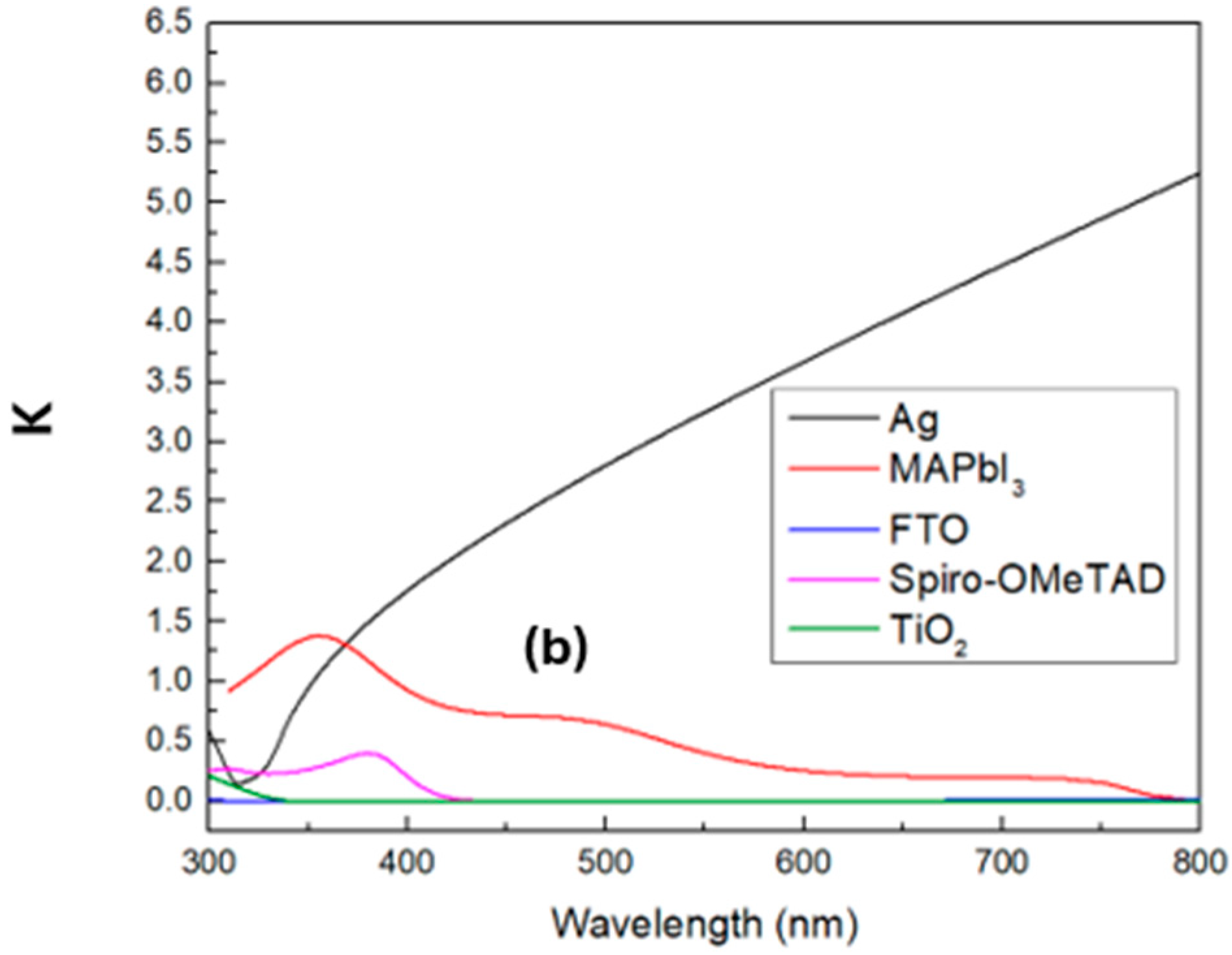
Figure 9a,b illustrate the real as well as the imaginary parts of the refraction index for each layer of the PSC structure referenced in the pertinent literature [24,25]. We applied this data as an interpolation function based on the wavelength of light and incorporated it into the optical variables of the simulated structure.
The bandgap energy value (Eg) presented in Table 5 represents the effective energy gap of the materials at room temperature. However, the influence of temperature variations on the energy gap values was addressed by acquiring collected information from the pertinent literature [26,27,28,29,30] and incorporating them as interpolated temperature values into the material characteristics. Numerous investigational projects have confirmed that Fe doping decreases the optical bandgap of SnO2 from around 3.6 eV to standards near 3.0 eV subject to doping attentiveness and manufacture circumstances [31,32].
Table 5. Proposed PSC parameters.
ParametersFTOTiO2SnO2MAPbI3Spiro-OMeTAD
Thickness (nm)1005040330350
ε r 999 6.5 3
E g ( e V )3.53.23.6/3.03(SnO2/Fe-doped SnO2) 1.55 3
χ ( e V )444 3.93 2.45
N v ( c m 3 ) 1.8 × 10 19 1.8 × 10 19 1.8 × 10 19 3.9 × 10 18 1 × 10 20
N c ( c m 3 ) 2.2 × 10 18 2 × 10 18 2.2 × 10 18 2.75 × 10 18 1 × 10 20
μ n / μ p ( c m 2 / V s ) 20/1020/10100/25 50 / 50 2/0.1
N A ( c m 3 )--- 3 × 10 15 2 × 10 18
N D ( c m 3 ) 2 × 10 19 9 × 10 16 1 × 10 17 --
Ref.[12,20][20,23][31,32][20,23][20,25]
Ref of refractive index[33][33][33][24][33]

3.1.3. Physical Theory

To investigate the optical and electrical properties of the PSC, we conducted FEM-based research utilizing radio-frequency and semiconductor COMSOL modules. The simulation was initially computed using the parameters shown in Table 5 and then recomputed with varying temperature values and absorber and transporter layer thicknesses. For the optical investigation, as mentioned previously, the input solar power provided to the cell’s top side was added using conventional AM1.5G quantities as a plane waveform with an interpolated function based on the incident light spectrum. The Floquet boundary conditions were applied to each of the structure’s two facing sides to create a unit cell with identical width and depth that can be repeated in both vertical axes to minimize calculation time.
The Helmholtz wave equation, which was obtained from the frequency domain of Maxwell’s formula, was solved to ascertain the electric field value via the several PSC layers [23]:
× ( × E ) k 0 2 ε r   E = 0
where E, k0, and εr stand for the material’s electric field, wave number, and dielectric constant, respectively. The refractive index value determines a material’s relative permittivity, which may then be seen as a function of incident light wavelength as follows [23]:
ε r = ε + j ε = ( n ( λ ) j k ( λ ) ) 2
The real and imaginary values of relative permittivity are represented by ε′ and ε″, respectively. Thus, n and k in a function of the wavelength are represented in Figure 9.
The local spectral carrier generation rate G(x,λ) within the MAPbI3 absorber layer is calculated from the absorbed electromagnetic energy density. The energy absorbed per unit volume is proportional to the imaginary part of the permittivity and the square of the electric field magnitude [21]:
G ( x , λ ) = ω ε 0 ε ( λ ) 2 | E ( x , λ ) | 2 = ε 0 c n ( λ ) k ( λ ) λ       | E ( x , λ ) | 2
where ħ represents the Plank’s constant, ε 0 is the vacuum permittivity, c is the speed of light, and λ is the photon energy. This calculation is automatically performed by the Wave Optics Module.
To obtain the total steady-state photogeneration rate G ( x ) required for the Semiconductor Module, the spectral generation rate G ( x , λ ) is integrated over the standardized AM1.5G solar spectrum Φ AM 1.5 G ( λ ) across the relevant absorption range ( λ m i n = 300   nm   t o λ m a x = 1000   nm ) [21]:
G t o t = G n = G p = λ m i n λ m a x G ( x , λ ) , Φ AM 1.5 G ( λ ) d λ
where G n and G p are the electron and hole generation rates.
The below equation represents the estimation of the SC’s absorption that is settled using the S-parameters [21]:
A b s o r p t i o n = 1 | S 11 | 2 | S 21 | 2
where | S 11 | 2 and | S 21 | 2 are, respectively, the transmission and reflection of the light wave.
In the semiconductor electrical analysis, Poisson’s and continuity equations were resolved utilizing the semiconductor COMSOL module to ascertain the PSCs open-circuit voltage and short-circuit current density as follows [21]:
. ( ε 0 ε r φ ) = ρ
n t = 1 q J n + G n R n
p t = 1 q J p + G p R p
where q is the electron charge, ε0 is the vacuum permittivity, φ is the electrostatic potential, and ρ is the charge density [21]:
ρ = q ( n p N D + N A )
where the concentrations of electrons and holes are denoted by n and p, respectively.
Current densities of electrons and holes are calculated using the drift-diffusion model in the manner described below [21]:
J n = q μ n n φ + q D n n
J p = q μ p p φ q D p p
Since intrinsic carrier density varies with temperature in the following ways, it was considered when examining the impact of temperature on PSC electrical performance:
n i = N c N v e E g ( T ) / K T
where n i , N c , N v , E g , K and T are the concentrations of the intrinsic carriers, the conduction and valence bands of the state’s density, band gap energy, the constant of Boltzmann and the temperature, respectively.
The overall carrier loss rate R within the active perovskite layer is the sum of three distinct physical mechanisms, reflecting the complex recombination kinetics characteristic of hybrid perovskites:
R = R SRH + R rad + R Auger
Shockley–Read–Hall (SRH) Recombination ( R SRH ) : This non-radiative, defect-assisted recombination dominates carrier loss, especially at trap-rich interfaces and grain boundaries. Assuming a single defect level near the mid-gap [34,35],
R SRH = n p n i 2 τ p 0 ( n + n 1 ) + τ n 0 ( p + p 1 )
For MAPbI 3 , typical bulk SRH lifetimes ( τ n 0 , τ p 0 ) are set to 500   ns . The thermal carrier densities n 1   a n d   p 1 are assumed equal to the intrinsic carrier concentration n i for a mid-gap defect level.
Radiative Recombination ( R rad ) : This is the intrinsic band-to-band recombination that governs the theoretical maximum open-circuit voltage:
R rad = B ( n p n i 2 )
A radiative recombination coefficient of B = 8 × 10 10   cm 3 / s is used for MAPbI 3 .
Auger Recombination ( R Auger ) : This three-carrier process involves energy transfer to a third carrier, dominant only at extremely high carrier densities:
R Auger = C n ( n 2 p n n i 2 ) + C p ( p 2 n p n i 2 )
Auger coefficients are typically very small for perovskites, employed here primarily for model completeness, set at C n = C p = 1 × 10 28   cm 6 / s . .
(Xia et al. 2021) have demonstrated experimentally and analytically that the lead-halide perovskite carriers’ mobilities are nearly constant for temperatures above 300 K, even though the carrier displacement of semiconductor materials are temperature-dependent factors [35]. Then, over the selected temperature range in our investigation, the change in carrier mobilities induced on by temperature variation can be disregarded.

3.1.4. Boundary Conditions

The front FTO electrode is modelled as an ideal ohmic contact, ensuring negligible contact resistance relative to the overall device resistance. This condition assumes local thermodynamic equilibrium at the boundary, pinning the electron and hole concentrations ( n , p ) to their equilibrium values ( n e q , p e q ) .
The back Ag electrode contact to the Spiro-OMeTAD (HTL) is modelled as a Schottky contact. The Fermi level is set by the Ag work function ( Φ Ag 4.3   eV ) . This establishes a built-in potential barrier Φ B against hole extraction at the contact interface, although the HTL is doped p -type to minimize this barrier.
Interface SRV ( S n , p ) is explicitly used at the ETL / MAPbI 3 and MAPbI 3 / HTL interfaces to model recombination via interface traps. While the manuscript references a high velocity of 10 7   cm / s , realistic simulation requires adjusting these values to achieve the measured high efficiencies, typically in the range of 10 3 10 5   cm / s for state-of-the-art PSCs, unless specific material interactions or high defect densities are modelled. For Device 2, the SRV at the Fe - SnO 2 / MAPbI 3 interface is significantly reduced compared to Device 1, reflecting the observed defect passivation.
For the optical simulation, Floquet periodic boundary conditions are applied to the lateral boundaries of the 2 D unit cell. This condition ensures that the calculated optical field profile accurately represents light propagation through an infinite, perfectly periodic planar stack, minimizing computational load while maintaining physical fidelity.

3.1.5. Meshing and Convergence

A free triangular mesh is employed across the 2 D geometry. A fine mesh resolution is essential in regions where solution variables (potential, carrier concentration, generation rate) exhibit steep gradients, particularly across the absorber layer and at all hetero interfaces. A minimum of five mesh elements is ensured across the thickness of the thinnest layers ( SnO 2 , TiO 2 ) . Furthermore, Boundary Layer Meshing is implemented at the ETL / MAPbI 3 and MAPbI 3 / HTL interfaces to accurately resolve the potential and concentration changes associated with band bending and localized charge accumulation. The MAPbI 3 absorber layer is assigned to be a maximum element size much smaller than the diffusion length to ensure accurate resolution of carrier dynamics.

3.1.6. Solver Specifications

The inherent nonlinearity and strong coupling between the electric potential ( ϕ ) , electron concentration (n), and hole concentration (p) in the drift-diffusion model necessitates a robust solution strategy. While a fully coupled approach provides maximum convergence stability by solving the entire system of variables simultaneously (large Jacobian matrix), the computational complexity of the coupled optoelectronic–thermal system benefits from a segregated approach. The model first solves the optical problem (wave optics) to determine G(x). Subsequently, the electrical problem (Poisson and continuity equations) is solved, often using an iterative segregated scheme that groups ( ϕ ) into one step and (n, p) into another, optimizing computational memory usage.
The algebraic system resulting from the FEM discretization is solved using a direct linear solver, specifically the PARDISO solver, which is highly efficient for sparse matrices encountered in stationary solutions. The nonlinear iterations are controlled by a relative tolerance criterion of 10 4 . A nonlinear damping factor (typically 0.9) is applied automatically by the algorithm to aid convergence in challenging regions, such as interfaces with abrupt band bending.

4. Conclusions

This work established a rigorous computational framework to elucidate the role of interface engineering in optimizing the performance of planar perovskite solar cells. The comparative analysis of single-layer TiO2 versus bi-layer TiO 2 / SnO 2 and TiO 2 / SnO 2 : Fe architectures confirmed that the introduction of a secondary metal oxide layer significantly mitigates the limitations of traditional TiO2 ETLs, such as low electron mobility and hysteresis. Specifically, the TiO 2 / SnO 2 : Fe configuration demonstrated the most robust photovoltaic parameters, driven by an upward shift in the conduction band minimum that improves energetic alignment with the MAPbI3 absorber.
The simulation identified a critical trade-off in device physics: Fe doping, resulting in enhancement in the internal electric field and carrier extraction velocity, dominates the device kinetics, leading to a net gain in open-circuit voltage (VOC) and fill factor. Moreover, the Fe-doped device exhibited superior thermal operating performance, minimizing efficiency degradation at elevated temperatures (440 K).
Future research directions will focus on two parallel tracks. First, investigations will target passivation strategies at the hole transport layer (HTL) interface to suppress non-radiative recombination losses. Second, and most critically, this study will transition from numerical modelling to experimental realization. The immediate next phase will involve the fabrication and characterization of the proposed TiO 2 / SnO 2 : Fe bi-layer architectures to empirically validate the predicted efficiency gains and corroborate the thermal-stability profiles under real-world operating conditions.

Author Contributions

Conceptualization, S.A. and A.A.Z.; methodology, S.A., M.A., M.A.A. and A.A.Z.; software, S.A., M.A., M.A.A. and B.Y.; validation, S.A., M.A., M.A.A., B.Y. and A.A.Z.; formal analysis, S.A., M.A., M.A.A., B.Y. and A.A.Z.; investigation, S.A., M.A., M.A.A., B.Y. and A.A.Z.; writing—original draft preparation, M.A., M.A.A., S.A. and A.A.Z.; writing—review and editing, M.A., M.A.A., S.A., A.A.Z. and B.Y.; visualization, M.A., M.A.A., S.A., A.A.Z. and B.Y.; supervision, B.Y.; project administration, S.A.; funding acquisition, S.A. All authors have read and agreed to the published version of the manuscript.

Funding

This research was funded by Onaizah Colleges, Saudi Arabia, and the APC was funded by Onaizah Colleges, Saudi Arabia.

Institutional Review Board Statement

Not applicable.

Informed Consent Statement

Not applicable.

Data Availability Statement

The original contributions presented in this study are included in the article. Further inquiries can be directed to the corresponding author.

Acknowledgments

The authors express their sincere gratitude and appreciation to Onaizah Colleges, Saudi Arabia, for providing APC funding for this research.

Conflicts of Interest

The authors declare no conflicts of interest.

References

  1. Lazaroiu, A.C.; Gmal Osman, M.; Strejoiu, C.-V.; Lazaroiu, G. A Comprehensive Overview of Photovoltaic Technologies and Their Efficiency for Climate Neutrality. Sustainability 2023, 15, 16297. [Google Scholar] [CrossRef] [Scilit]
  2. Raju, T.D.; Murugadoss, V.; Nirmal, K.A.; Dongale, T.D.; Kesavan, A.V.; Kim, T.G. Advancements in perovskites for solar cell commercialization: A review. Adv. Powder Mater. 2025, 4, 100275. [Google Scholar] [CrossRef] [Scilit]
  3. Solar Cells Efficiency Map. Available online: https://www.nlr.gov/pv/cell-efficiency (accessed on 25 October 2025).
  4. Sharma, R.; Sharma, A.; Agarwal, S.; Dhaka, M.S. Stability and efficiency issues, solutions and advancements in perovskite solar cells: A review. Sol. Energy 2022, 244, 516–535. [Google Scholar] [CrossRef] [Scilit]
  5. Sharma, A.; Sharma, R.; Agarwal, S.; Dhaka, M.S. Role of transport layers in efficiency enhancement of perovskite solar cells. Renew. Sustain. Energy Rev. 2025, 222, 115795. [Google Scholar] [CrossRef] [Scilit]
  6. Al Atem, M.; Rezgui, B.D.; Touhami, I.; Bouaïcha, M. Numerical simulation and optimization of high-performance lead-based FAMACsPb(IBr)3 perovskite solar cells using SCAPS 1D. Results Eng. 2026, 29, 108555. [Google Scholar] [CrossRef] [Scilit]
  7. Abdelrazek, A.S.; El-Sehiemy, R.A.; Rezk, H.; Ghoniem, R.M.; Falaras, P.; Zaky, A.A. Dynamic Electrical Models of Perovskite Solar Cells Considering Hysteresis and Charge Accumulations Effects by Using Equilibrium Optimizer. IEEE Access 2022, 10, 104111–104122. [Google Scholar] [CrossRef] [Scilit]
  8. Al Atem, M.; Makableh, Y. Towards Sustainable Perovskite Solar Cells: Lead-Free High Efficiency Designs with Tin and Germanium. Eng 2025, 6, 38. [Google Scholar] [CrossRef] [Scilit]
  9. Hoang Huy, V.P.; Bark, C.-W. Review on Surface Modification of SnO2 Electron Transport Layer for High-Efficiency Perovskite Solar Cells. Appl. Sci. 2023, 13, 10715. [Google Scholar] [CrossRef] [Scilit]
  10. Song, J.W.; Shin, Y.S.; Kim, M.; Lee, J.; Lee, D.; Seo, J.; Lee, Y.; Lee, W.; Kim, H.-B.; Mo, S.-I.; et al. Post-Treated Polycrystalline SnO2 in Perovskite Solar Cells for High Efficiency and Quasi-Steady-State-IV Stability. Adv. Energy Mater. 2024, 14, 2401753. [Google Scholar] [CrossRef] [Scilit]
  11. Huang, X.; Hu, Z.; Xu, J.; Wang, P.; Wang, L.; Zhang, J.; Zhu, Y. Low-temperature processed SnO2 compact layer by incorporating TiO2 layer toward efficient planar heterojunction perovskite solar cells. Sol. Energy Mater. Sol. Cells 2017, 164, 87–92. [Google Scholar] [CrossRef] [Scilit]
  12. Guo, P.; Xu, L.; Yu, T.; Zhao, P.; Xu, J.; Shen, B. Transition metal in-situ doped BiOBr: Introducing oxygen vacancies to enhance hydroxyl radical generation for improved photocatalytic degradation of toluene. Sep. Purif. Technol. 2025, 354, 129247. [Google Scholar] [CrossRef] [Scilit]
  13. Sambasivam, S.; Obaidat, I.M. Effect of iron doping on ESR and Raman spectra of SnO2 nanomaterials. Mater. Today Proc. 2020, 28, 587–590. [Google Scholar] [CrossRef] [Scilit]
  14. Rezk, H.; Elsenety, M.M.; Ferahtia, S.; Falaras, P.; Zaky, A.A. A novel parameter identification strategy based on COOT optimizer applied to a three-diode model of triple cation perovskite solar cells. Neural Comput. Appl. 2023, 35, 10197–10219. [Google Scholar] [CrossRef] [Scilit]
  15. Zaky, A.A.; Fathy, A.; Rezk, H.; Gkini, K.; Falaras, P.; Abaza, A. A Modified Triple-Diode Model Parameters Identification for Perovskite Solar Cells via Nature-Inspired Search Optimization Algorithms. Sustainability 2021, 13, 12969. [Google Scholar] [CrossRef] [Scilit]
  16. Wang, Z.; Gong, C.; Zhang, C.; Zhao, C.; Su, T.-S.; Li, H.; Zhang, H. Recent advances in interfacial engineering for high efficiency perovskite photovoltaics. DeCarbon 2025, 8, 100107. [Google Scholar] [CrossRef] [Scilit]
  17. Dawoud, S.M.; Selim, F.; Lin, X.; Zaky, A.A. Techno-Economic and Sensitivity Investigation of a Novel Perovskite Solar Cells Based High Efficient Hybrid Electric Sources for Off-Shore Oil Ships. IEEE Access 2023, 11, 41635–41643. [Google Scholar] [CrossRef] [Scilit]
  18. Suchikova, Y.; Nazarovets, S.; Konuhova, M.; Popov, A.I. Binary Oxide Ceramics (TiO2, ZnO, Al2O3, SiO2, CeO2, Fe2O3, and WO3) for Solar Cell Applications: A Comparative and Bibliometric Analysis. Ceramics 2025, 8, 119. [Google Scholar] [CrossRef] [Scilit]
  19. Alyahya, S.; Arnaout, M.; Al Atem, M.; Alanazi, M.A.; Yousif, B.; Zaky, A.A. Performance and Stability Enhancement of Perovskite Solar Cells Based on Iron- Doped Bi-Electron Transport Layers. Inorganics 2026, 14, 118. [Google Scholar] [CrossRef] [Scilit]
  20. Saxena, P.; Gorji, N.E. COMSOL simulation of heat distributionin perovskite solar cells: Coupled optical–electrical–thermal 3-D analysis. IEEE J. Photovolt. 2019, 9, 1693–1698. [Google Scholar] [CrossRef] [Scilit]
  21. Zandi, S.; Razaghi, M. Finite element simulation of perovskite solar cell: A study on efficiency improvement based on structural and material modification. Sol. Energy 2019, 179, 298–306. [Google Scholar] [CrossRef] [Scilit]
  22. Minemoto, T.; Murata, M. Device modeling of perovskite solar cells based on structural similarity with thin film inorganic semiconductor solar cells. J. Appl. Phys. 2014, 116, 2–8. [Google Scholar] [CrossRef] [Scilit]
  23. Jahantigh, F.; Ghorashi, S.M.B. Optical simulation and investigation of the effect of hysteresis on the perovskite solar cells. Nano 2019, 14, 1950127. [Google Scholar] [CrossRef] [Scilit]
  24. Raoult, E.; Bodeux, R.; Jutteau, S.; Rives, S. Optical characterizations and modelling of semitransparent perovskite solar cells for tandem applications. In Proceedings of the 36th European Photovoltaic Solar Energy Conference and Exhibition, Marseille, France, 9–13 September 2019; Volume 36, pp. 757–763. [Google Scholar] [CrossRef]
  25. Manzoor, S.; Häusele, J.; Bush, K.A.; Palmstrom, A.F.; Carpenter, J.; Yu, Z.J.; Mcgehee, M.D.; Holman, Z.C. Optical modeling of wide-bandgap perovskite and perovskite/silicon tandem solar cells using complex refractive indices for arbitrary-bandgap perovskite absorbers. Opt. Exp. 2018, 26, 27441. [Google Scholar] [CrossRef] [Scilit] [PubMed]
  26. Mishra, V.; Warshi, M.K.; Sati, A.; Kumar, A.; Mishra, V.; Kumar, R.; Sagdeo, P.R. Investigation of temperature-dependent optical properties of TiO2 using diffuse reflectance spectroscopy. Soc. Netw. Appl. Sci. 2019, 1, 1–8. [Google Scholar] [CrossRef] [Scilit]
  27. Foley, B.J.; Marlowe, D.L.; Sun, K.; Scudiero, L.; Gupta, M.C.; Choi, J.J. Temperature dependent energy levels of methylammonium lead iodide perovskite. Appl. Phys. Lett. 2015, 106, 581–586. [Google Scholar] [CrossRef] [Scilit]
  28. Cho, Y.; Yamaguchi, A.; Uehara, R.; Yasuhara, S.; Hoshina, T.; Miyauchi, M. Temperature dependence on bandgap of semiconductor photocatalysts. J. Chem. Phys. 2020, 152, 231101. [Google Scholar] [CrossRef] [Scilit] [PubMed]
  29. Al Atem, M.; Makableh, Y.; Arnaout, M. Analytical Solutions for Current–Voltage Properties of PSCs and Equivalent Circuit Approximation. Eng 2025, 6, 62. [Google Scholar] [CrossRef] [Scilit]
  30. Albuloushi, A.; Lari, F.; Alawadhi, F.; Hussain, M.; Sadeq, Z.; Al Atem, M. Numerical Design and Charge Transport Layer Optimization of Lead-Free Cs3Sb2I9 PSCs: Toward Experimental Efficiency Enhancement. Eng 2026, 7, 234. [Google Scholar] [CrossRef] [Scilit]
  31. Arnaout, M.; Salameh, W.; Assi, A.; Chahine, K. My PV tool: A Matlab-based tool to study the series and shunt resistances in photovoltaic modules. In Proceedings of the 2016 3rd International Conference on Renewable Energies for Developing Countries (REDEC), Zouk Mosbeh, Lebanon, 13–15 July 2016; pp. 1–6. [Google Scholar] [CrossRef] [Scilit]
  32. Sharma, M.; Kumar, S.; Alvi, P.A. Role of Fe (Transition Metal) in Tuning the Optical Behavior of SnO2 Nanoparticles. In 2020 International Conference on Emerging Trends in Communication, Control and Computing (ICONC3); IEEE: New York, NY, USA, 2020; pp. 1–4. [Google Scholar]
  33. Matysiak, W.; Tański, T.; Smok, W. Study of optical and dielectric constants of hybrid SnO2 electrospun nanostructures. Appl. Phys. A 2020, 126, 115. [Google Scholar] [CrossRef] [Scilit]
  34. Tabrizi, A.A.; Saghaei, H.; Mehranpour, M.A.; Jahangiri, M. Enhancement of absorption and effectiveness of a perovskite thin-film solar cell embedded with gold nanospheres. Plasmonics 2021, 16, 747–760. [Google Scholar] [CrossRef] [Scilit]
  35. Xia, C.Q.; Peng, J.; Poncé, S.; Patel, J.B.; Wright, A.D.; Crothers, T.W.; Borchert, J.; Milot, R.L.; Kraus, H.; Lin, Q.; et al. Limits to electrical mobility in leadhalideperovskite semiconductors. J. Phys. Chem. Lett. 2021, 12, 3607–3617. [Google Scholar] [CrossRef] [Scilit] [PubMed]
Figure 1. Band diagram of different PSC structures. (a) Reference. (b) Device 1. (c) Device 2.
Inorganics 14 00196 g001
Figure 2. Optical properties for the three devices. (a) Absorption profiles. (b) EQE spectra.
Inorganics 14 00196 g002
Figure 3. (a) J-V curves for the investigated devices; (b) P-V curves for the investigated devices.
Inorganics 14 00196 g003
Figure 4. PSC parameters depend on proposed PSC at different temperatures.(a) The change of PCE with temperature; (b) The change of short circuit current against temperature; (c) The change of fill factor against temperature; (d) The change of open circuit voltage against temperature.
Inorganics 14 00196 g004aInorganics 14 00196 g004b
Figure 5. Electron and hole densities across the PCS at (a,d) reference, (b,e) Device 1, and (c,f) Device 2, respectively.
Inorganics 14 00196 g005
Figure 6. Electric field distribution.
Inorganics 14 00196 g006
Figure 7. Electric potential distribution.
Inorganics 14 00196 g007
Figure 8. Device structure and energy level: (a,d) reference device, (b,e) Device 1, and (c,f) Device 2.
Inorganics 14 00196 g008
Figure 9. Refractive indices of (a) the real and (b) imaginary part for FTO, Ag, TiO2, MAPbI3 perovskite, and Spiro-OMeTAD.
Inorganics 14 00196 g009aInorganics 14 00196 g009b
Table 1. Integrated optical quantities for investigated devices.
DeviceIntegrated
EQE (%)
Average Visible
Absorption
(400–700 nm) (%)
Solar-Weighted Visible
Absorption
(400–700 nm) (%)
Solar-Weighted
Absorption (%)
Calculated
Jsc (mA/cm2)
Ref 26.2176.4774.9328.6216.75
D1 26.2483.7582.6629.4116.77
D2 26.2484.2783.4629.5216.77
Table 2. Convergence analysis of investigated devices.
DeviceCoarseMediumFiner
Ref17.73817.69717.703
D117.95917.95817.961
D218.38118.3818.383
Table 3. Key performance indicators for the investigated PSCs.
ParameterReference (TiO2)Device 1 (TiO2/SnO2)Device 2 (TiO2/SnO2:Fe)
Jsc (mA cm−2)~17.8~18.0~18.1
Voc (V)~1.16~1.17~1.18
FF (%)~84~84.5~85
PCE (%) at 300 K17.518.018.3
PCE (%) at 440 K12.312.713
PCE Degradation (%)29.72928.9
Peak Electric Field (V m−1)~4.0 × 10⁶~4.0 × 10⁶>4.5 × 10⁶
Maximum SRH Recombination Rate (m−3 s−1)~7 × 1026~6 × 1026~8 × 1026
Table 4. PSC structures.
ReferenceDevice 1Device 2
FTO/TiO2/MAPbI3/Spiro-OMETAD/AgFTO/TiO2/SnO2/MAPbI3/Spiro-OMETAD/AgFTO/TiO2/SnO2 + Fe/MAPbI3/Spiro-OMETAD/Ag
Disclaimer/Publisher’s Note: The statements, opinions and data contained in all publications are solely those of the individual author(s) and contributor(s) and not of MDPI and/or the editor(s). MDPI and/or the editor(s) disclaim responsibility for any injury to people or property resulting from any ideas, methods, instructions or products referred to in the content.