Article

Nanocrystalline–Amorphous Transition in ZrN Nanofilms Induced by Helium Accumulation at Grain Boundaries

1
Department of Scientific Research, The People’s Hospital of Guangxi Zhuang Autonomous Region, Nanning 530021, China
2
School of Mathematics and Physics, Mianyang Teachers’ College, Mianyang 621000, China
3
School of Mechanical Engineering, Hefei University of Technology, Hefei 230009, China
4
Guangxi Key Laboratory of Natural Polymer Chemistry and Physics, College of Chemistry and Materials, Nanning Normal University, Nanning 530001, China
*
Authors to whom correspondence should be addressed.
These authors contributed equally to this work.
Inorganics 2025, 13(5), 158; https://doi.org/10.3390/inorganics13050158
Submission received: 29 March 2025 / Revised: 28 April 2025 / Accepted: 7 May 2025 / Published: 9 May 2025
(This article belongs to the Special Issue Recent Research and Application of Amorphous Materials)

Abstract

:
Helium (He) accumulation, a byproduct of nuclear transmutation, poses a significant reliability challenge for the materials used in nuclear reactors. Nanomaterials, with their high density of interfaces, offer superior He tolerance by absorbing He atoms and suppressing bubble growth. However, the long-term stability of these materials under continuous He accumulation remains a concern. This study investigated the microstructural and mechanical property responses of ZrN nanofilms to excessive He accumulation. Different doses of He atoms were introduced via magnetron sputtering. The results indicate that increasing the He dose induced a nanocrystalline-to-amorphous transition and instability in the mechanical properties. The structural and mechanical instability, characterized by surface blistering, softening, abnormal lattice shrinkage, and amorphization, was primarily triggered by the degradation of the grain boundaries with He accumulation, and an amorphization model of nanomaterials is proposed.

1. Introduction

Under high-energy and high-flux neutron irradiation, reactor materials often undergo severe amorphization, leading to comprehensive performance degradation. To improve the radiation tolerance of nuclear materials, the idea of radiation-resistant nanomaterials has been proposed in recent years [1,2,3,4]. It uses high-density interfaces to inhibit the aggregation of radiation-induced point defects and accelerate their annihilation [5]. For example, oxide dispersion-strengthened (ODS) steels [6], multilayered materials [7], high-entropy alloys with nanoprecipitates [8], etc., have been reported that can annihilate defects and maintain a stable structure under radiation.
However, most of the research on radiation-tolerant nanomaterials has focused more on the damage caused by the atomic collision cascade of high-energy particles. In fact, as the energy and fluence of neutrons increase, the accumulation damage of transmutational products like He nuclei cannot be ignored [9,10]. The accumulation of He atoms can lead to the severe destruction of the structure and performance of nuclear materials [11]. Specifically, He atoms can trap themselves in vacancies to form He clusters (He bubbles), which introduce compressive stress into solids. With the bubbles’ growth, cracks could form and evolve into cavities gradually, resulting in material embrittlement [12], surface blistering [13], etc., thus reducing the long-term reliability of nuclear materials.
Although some studies have shown that high-density grain boundaries in nanomaterials can significantly adsorb He bubbles and inhibit their growth in grains, giving nanomaterials superior tolerance to He accumulation damage [1,2,3,4], other researchers have reported some opposite conclusions. For example, when implanted with 10 keV He+ ions at an average flux of 1013 He+/cm2s, large He-filled cavities can be formed in the grains of nanocrystalline nickel, facilitated by the radiation-induced vacancy clusters [14]. He accumulation can lead to surface blistering on the surface of nanocrystalline ZrN after He implantation and annealing at 600~1000 °C [15]. Chen et al. reported that with the implantation of 65 keV He+ ions at 277 °C, and subsequent irradiation with 9 MeV Au ions (10 dpa) at 700 °C, He bubbles expanded obviously in nanocrystalline SiC, while no bubbles were found in a single-crystal SiC under the same irradiation conditions [16]. These findings suggest that the stability of nanomaterials under different He accumulation conditions needs to be evaluated carefully.
The stability of nanomaterials under He accumulation largely depends on the interaction behavior between the He atoms and grain boundaries [1,2,3,4]. However, the prevailing method to evaluate He accumulation damage is He+ ion irradiation. Since ion irradiation will introduce inhomogeneous defects, thermal effects, and surface effects (limited depth of implantation) into the samples, it brings more challenges to quantitative studies on the pure interaction of He atoms and interfaces in nanomaterials, and increases the complexity of the failure behavior of nanomaterials. To investigate the pure interaction of grain boundaries and He atoms in nanomaterials, we tried to exclude the influence of inhomogeneous radiation defects and temperature and surface effects by introducing different doses of He atoms uniformly into ZrN nanofilms during film deposition, by magnetron sputtering at room temperature [17]. With this method, we evaluated the stability of ZrN nanofilms under severe He accumulation in this study, as ZrN is a promising radiation-tolerant material, especially as a candidate material for nuclear fuel cladding and other reactor structural components [18,19]. We demonstrate that He accumulation degrades the grain boundaries in ZrN nanofilms, driving amorphization and performance deterioration.

2. Results

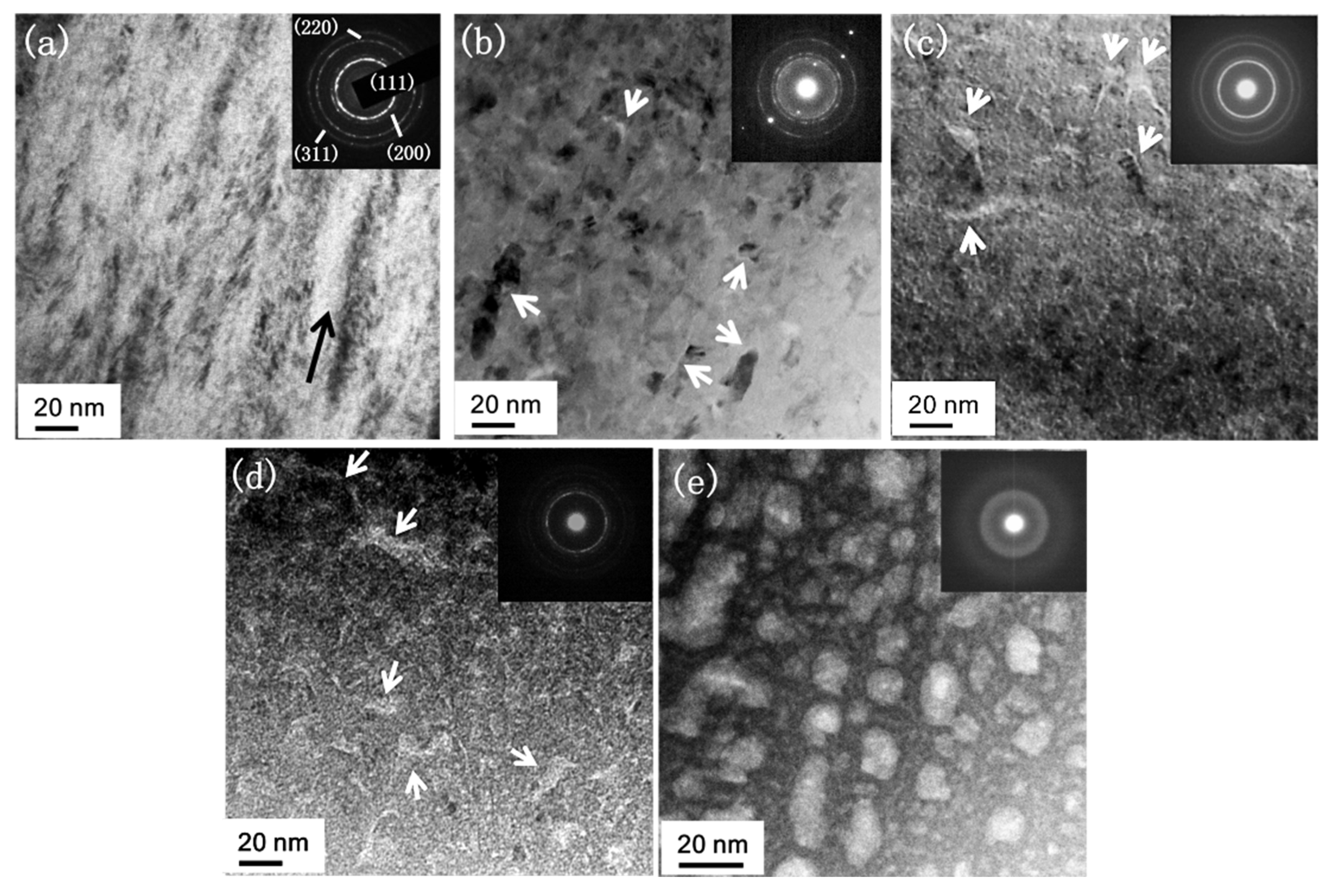
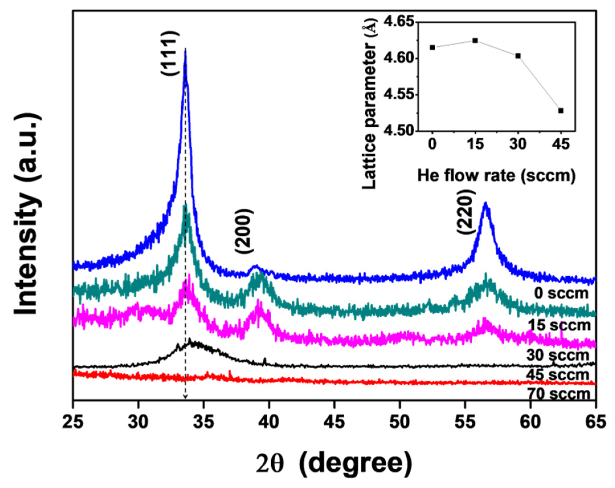
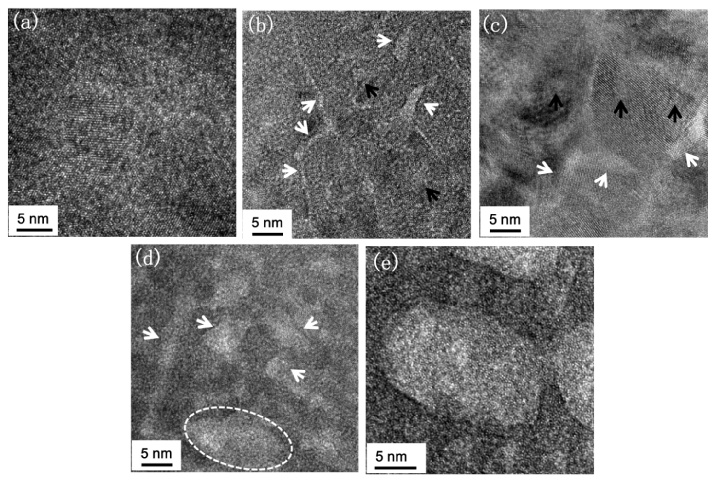
2.1. Microstructure Evolution with He Accumulation

The typical GIXRD spectra of the ZrN nanofilms, obtained with He flow rates ranging from 0 to 70 standard cubic centimeters per minute (sccm), are shown in Figure 1. It was found that as the He flow rate increased, the full width at the half maximum of the peak became wider. Moreover, surface blistering on the specimen has become increasingly apparent with the He flow rate increasing (Figure 2). From the TEM images (Figure 3), it can be seen that the crystallite size within the ZrN thin films did not change significantly with the He flow rates, indicating the XRD peak broadening was substantially influenced by factors beyond the crystallite size, most likely by the non-uniform microstrain and decreased crystallinity induced by the He implantation. At an He flow rate of 45 sccm, the diffraction peaks broadened dramatically, showing that the crystallinity of the ZrN nanofilms decreased obviously. In particular, as the He flow rate increased to 70 sccm, all the peaks disappeared, indicating severe amorphization in the ZrN nanofilms. The peak positions of the different planes in the samples were obtained and converted to lattice parameters by using the software Jade 6.0. As shown in the inserted picture in Figure 1, the lattice parameters of the ZrN nanofilms with an He flow rate of 15 sccm increased slightly compared with the original ZrN. Then, it reduced sharply, from 4.63 Å to 4.52 Å, at an He flow rate of 45 sccm. The obvious shift of the (111) peak for the sample (45 sccm) toward a higher angle (marked by a dashed line) also verifies the lattice shrinkage. The abnormal lattice shrinkage followed by amorphization implies that the He flow rate of 45 sccm may be the threshold at which severe He cumulative damage occurred in the ZrN nanofilms under our synthesis conditions.
It is worth noting that many studies have shown that He accumulation often leads to lattice swelling, which can be attributed to the interstitial He atoms squeezing the lattice [11,18]. However, there was no monotonic increasing relationship between the lattice constant and the He dose in this study or in some other reports [17,18,19,20,21]. We will discuss this later, combining it with other findings.

2.2. Blistering on the Surface of ZrN Nanofilms

Prevalent blistering was found on the film surfaces at He flow rates above 45 sccm (Figure 2d,e), while the ZrN nanofilms had relatively flat and smooth surfaces (Figure 2a–c) below the threshold of 45 sccm. As we know, blistering on the surface is a typical pattern of He accumulation damage, resulting from the release of He atoms and other interstitial atoms diffusing from the interior of the sample [17]. Lattice shrinkage and blistering happening at the same time implies a close relationship between these two damage behaviors. It is reasonable to suspect that noticeable lattice shrinkage can predict a qualitative change in the microstructure of nanofilms, which may trigger severe He accumulation damage.
Figure 2. Surface morphology of the (a) as-deposited ZrN nanofilm and (b) He-implanted ZrN nanofilm at 15 sccm, (c) 30 sccm, (d) 45 sccm, and (e) 70 sccm, showing that blisters appear as the He flow rate increases.
Inorganics 13 00158 g002

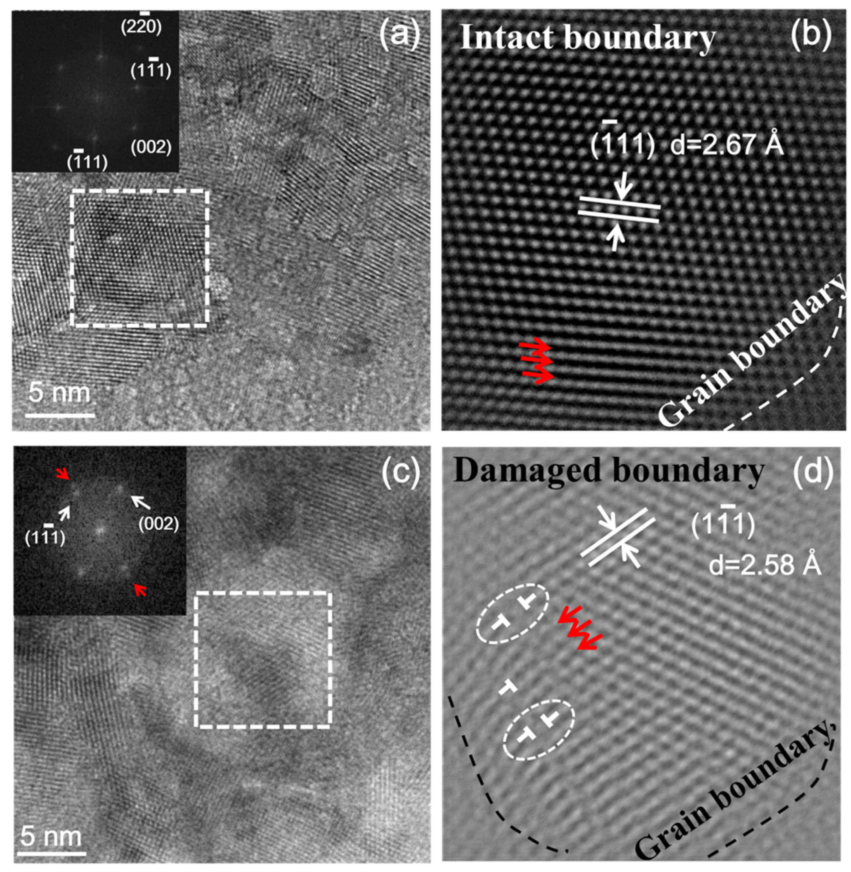
2.3. Interaction of He Bubbles and Grain Boundaries

To understand the microstructure evolution behavior as the He injection rate increased, we compared the cross-sectional TEM images of the samples with different He doses. Figure 3a shows the TEM image of the nanofilm without He injection. It can be seen that the columnar crystal structure inside the film is relatively intact. Moreover, the four sharp—(111), (200), (220), and (311)—diffraction rings in the selected area electron diffraction (SAED) pattern (inset of Figure 3a) indicate that the ZrN nanofilm without He injection has better crystallinity. The columnar grains in the ZrN films were interrupted at the He flow rate of 15 sccm, resulting in more equiaxed grains of 10–20 nm in diameter, as shown in Figure 3b. Moreover, the initial He bubbles were mainly adsorbed at the grain boundaries in the form of strips (marked by white arrows). The strip-shaped He bubbles began to coarsen as the He dose increased (Figure 3c), but most of the He bubbles were still located along the grain boundaries. At the He flow rate of 45 sccm, a large number of irregular polygonal He bubbles can be observed in Figure 3d. Meanwhile, the grain boundaries became blurred and the He bubbles expanded from the grain boundaries toward the interior of the grain. We hypothesize that the irregular polygonal He bubbles formed when the bubbles, initially at the grain boundaries, began expanding into the grain interior as the grain boundary structure was compromised. We suggest that a residual pinning effect from the original grain boundary location, influenced by the interfacial energy, prevented the expanding bubble edges from fully relaxing into a spherical shape. The diffraction ring became blurred, indicating that its crystallinity had decreased severely (Figure 3d). As the He flow rate increased to 70 sccm, the He bubbles aggregated and expanded dramatically, while the grain boundaries disappeared and the irregular polygonal He bubbles became spherical (Figure 3e). The bubble shape changing indicates that the He bubbles were completely free from the grain boundaries and evolved to a spherical shape driven by the Gibbs free energy. This observation is supported by the diffraction rings (inset in Figure 3e). They transformed into halos, revealing that the nanocrystals underwent severe amorphization. This indicates that with increases in the He dose, the trapping (accommodating) effect of the grain boundaries on the He bubbles gradually weakens and then disappears, resulting in remarkable structural damage to the nanofilms.
Figure 3. Cross-sectional TEM images of the ZrN nanofilms: (a) the as-deposited ZrN nanofilm, (b) He-implanted ZrN nanofilm with 15 sccm, (c) He-implanted ZrN nanofilm with 30 sccm, (d) He-implanted ZrN nanofilm with 45 sccm, and (e) He-implanted ZrN nanofilm with 70 sccm. The black arrow shows the growth direction of the grain. The white arrows mark the He bubbles. The upper-right inset figures show the corresponding electron diffraction patterns.
Inorganics 13 00158 g003
The high-resolution transmission electron microscope (HRTEM) images reveal the interaction between the He atoms and grain boundaries. Figure 4a shows the intact grain boundaries of the nanofilms without He bubbles, while Figure 4b shows stripe-shaped He bubbles (indicated by the white arrows) distributed along the grain boundaries and a small amount of He bubbles (indicated by the black arrows) in the grain interior, which confirms the trapping effect of the grain boundary on the He bubbles, keeping the crystal structure stable at the He flow rate of 15 sccm. With an increase in the He dose, the strip-shaped He bubbles on the grain boundary began to gather and coarsen (Figure 4c). Note that the expansion of the spherical bubbles in the grain (indicated by the black arrows) is not obvious. This reveals that the growth of the He bubbles was still confined within the grain boundary at the He flow rate of 30 sccm. However, when the He flow rate increased to 45 sccm, as shown in Figure 4d, most of the stripe-shaped He bubbles along the grain boundaries grew into irregular polygonal bubbles (marked by the white arrows). And the bubbles expanded significantly toward the interior of the grains and swallowed up the bubbles in the grains forming larger He bubbles (the white dotted line). This shows the weak influence of the grain boundary on the He bubbles once the He dose surpasses the threshold. Finally, as the He dose increased, the grain boundary disappeared and the lattice structure was completely destroyed, showing an amorphous state (Figure 4e). Without the limitation of the grain boundary, the He bubbles spontaneously converged into a spherical shape to reduce the surface energy. The interaction behavior of the He bubbles and the grain boundary in Figure 4 is consistent with the experimental results shown in Figure 1, Figure 2 and Figure 3. It is rational to suspect that the weakening of the trapping effect of the grain boundary on the He bubbles was the essential factor leading to the severe He accumulation damage, including lattice shrinkage, amorphization, and blistering. And the He dose surpassing the threshold may have been the trigger for the degradation of the grain boundary.

2.4. Degradation of Grain Boundaries Induced by He Accumulation

To reveal the degradation mechanism of the grain boundary, we further analyzed the microstructure of typical grains at different He doses through HRTEM. Figure 5 presents the fast Fourier transform (FFT) and inverse Fourier transform (IFFT) of the HRTEM images within a selected area (within the dotted box). Figure 5a shows the HRTEM image of the film with the He flow rate of 15 sccm. At this low He dose, more He bubbles were located at the grain boundaries, with a few small bubbles in the grain interior (see the dotted box). From the FFT in the upper-left corner of Figure 5a, it can be seen that the diffraction spots in the crystal planes of the selected grain remain intact and regular. Furthermore, as shown in the IFFT (Figure 5b), the interplanar distance of the {111} plane is 2.67 Å in the grain, meaning the lattice constant of the selected grain is a little higher than that of the sample without He injection. The lattice swelling can be attributed to the small He bubbles squeezing the lattice in the grain (marked by the red arrows). However, the lattice swelling is limited and the lattice structure is intact because most of the He bubbles have been trapped in the grain boundaries. It is believed that the trapping effect of the grain boundary on He atoms can improve the resistance to He accumulation damage in ZrN nanofilms.
When the He flow rate was 45 sccm, the lattice changed greatly. The He bubbles broke free from the grain boundaries and expanded into the interior of the grain (the dotted box in Figure 5c). In the FFT corresponding to Figure 5c, the reciprocal lattice corresponding to the crystal plane is blurred, and satellite points (marked by the red arrows) appear. The two satellite points lie in the line of the reciprocal points of the {111} plane, but drift outward for a small distance. This indicates that part of the {111} plane collapsed, and lattice shrinkage occurred. The IFFT in Figure 5d shows that the collapse of the {111} planes occurred from the zone near the grain boundaries (marked by the red arrows) and expanded toward the grain interior, resulting in a decrease in the interplanar distance of the {111} plane to 2.58 Å.
It is important to note that a large number of vacancy-type defects (Figure 5d), like dislocations (marked by the Ts) and dislocation loops (marked by the dotted lines), appeared near the grain boundaries (periphery zone in Figure 5d), which were rarely found in the grain with a low He dose (Figure 5b). We believe it was the prevalence of the vacancy-type defects that destroyed the structure of the grain boundary, and weakened its trapping effect on the He bubbles. Plenty of the vacancy-type defects near the grain boundaries can be explained by the dislocation loop-punching mechanism [22]. At low He doses, more He-vacancy clusters preferentially accumulated within the grain boundaries because the energy barriers for point defect migration were lower at the interfaces than in the bulk [23]. And the growth of the He bubbles could be confined within the grain boundaries because the intact lattice structure near the interface inhibited the diffusion of the point defects. This resulted in more strip-shaped He bubbles growing along the grain boundaries and a few spherical He bubbles forming in the grain interior. As the He dose increased, no more space in the grain boundary was left for the He bubbles. Then, the strip-shaped bubbles tended to expand toward the grain interior by punching out dislocation loops constantly, leading to more vacancy-type defects forming near the interfaces. As the He dose increased to the threshold, the cumulative vacancy-type defects destroyed the lattice structure near the grain boundaries (Figure 5d), which reduced the ability of the interfaces to confine the He bubbles.
As the He bubbles expanded toward the grain interior, they merged with the bubbles in the grain (Figure 4d and Figure 5c). This process led to the release of the cumulative compressive stress induced by the He bubbles, which decreased the lattice constant [17,18,19,20,21]. Moreover, the destruction of the interface induced by the prevailing vacancy-type defects near the grain boundaries enhanced the short-circuiting diffusion. More interstitial atoms (like He atoms and self-interstitial atoms) tended to migrate along the grain boundaries toward the surface to further release the compressive stresses caused by the high-dose He injection. The migration of these massive interstitial atoms to the surface led to the lattice collapse (lattice shrinkage) and blistering of the ZrN nanofilms.
It is worthy to note that the He-induced lattice changes can also be readily interpreted from the perspective of macroscopic film stress evolution. At low He doses, the observed increase in the ZrN lattice parameter suggests the incorporation of interstitial He atoms, likely inducing compressive stress. Conversely, at higher He doses, pronounced grain boundary damage facilitated interstitial atoms diffusion and surface blistering. This process is typically associated with the formation of vacancy-type defects within a lattice, leading to a tendency toward tensile stress and observed lattice contraction.

2.5. Mechanical Properties of ZrN Nanofilms

As shown in Figure 6, the indentation hardness of the film without He injection is about 19 (Gpa), and the elastic modulus is about 185 (Gpa). The hardness and elastic modulus of the films with He are lower than those of the original one, and both of them decreased as the He dose increased. Especially when the He flow rate reached 45 sccm, both the hardness and elastic modulus dropped sharply. This is consistent with our supposition that the He flow rate of 45 sccm was the threshold for He accumulation damage in the films under our synthesis conditions.
The hardness deteriorated with an increase in the He dose in this study, which is contradictory to some previous studies. Many researchers have reported that the hardness of He-injected samples is positively correlated with the dose of the He injection [24]. This has been attributed to the defects introduced by the He bubbles hindering the movement of dislocations. However, both the hardness and elastic modulus of the ZrN nanofilms were inversely correlated with the He dose in this study, implying that dislocation movement may be no longer the main deformation mode of He-injected materials, which will be explained in the Section 3.

3. Discussion

Researchers often believe that high-density grain boundaries can improve the resistance to He accumulation damage. However, this study shows that as the He dose surpassed the threshold, the grain boundaries were preferentially destroyed, leading to severe amorphization and performance deterioration. Here, we propose a model for the various stages of He accumulation damage in nanomaterials, as shown in Figure 7. In the first stage, He accumulation in the nanomaterials is limited. The high density of the grain boundaries in the nanomaterials can adsorb the He atoms and inhibit the expansion of He bubbles toward the grains, thus improving the material’s resistance to He accumulation damage (Figure 7a). However, as the He accumulation increases to the threshold, the lattice structure of the grain boundaries and their neighboring zones are destroyed, resulting from the He bubbles expanding toward the grain interior. During this stage, the expansion of the He bubbles introduces more self-interstitial atoms near the grain boundaries, which diffuse along the grain boundaries to the surface, driven by the surface energy (Figure 7b). This leads to lattice shrinkage in the nanocrystalline structure and blistering on the surface, resulting in the deterioration of the mechanical performance. As the He accumulation increases continuously, the structure of the grain boundaries is severely destroyed. Out of the control of the grain boundaries, the He bubbles expand deeply into the grains, merging and growing dramatically. At the end of this stage, a huge amount of self-interstitial atoms are introduced by the expansion of the He bubbles, which can lead to the amorphization of the nanomaterials (Figure 7c).
This model can explain the degradation behavior of the hardness and elastic modulus of ZrN nanofilms with He accumulation (Figure 6). It has been reported that the deformation of nanomaterials can be more affected by the grain sliding, rotation, and dislocation emissions of the grain boundaries [25,26,27]. In this study, the grain boundaries in the ZrN nanofilms were destroyed by the prevailing vacancy-type defects (like dislocation loops) induced by the He accumulation. The degradation of the grain boundaries enhanced the sliding and rotation of the grains, and more dislocations were emitted from the grain boundaries (Figure 5d), resulting in a decrease in hardness. For the elastic modulus, the degradation was mainly related to the chemical bonds and crystal structure. The vacancy-type defects induced by the excessive He atoms weakened the chemical bonding force and destroyed the lattice structure near the grain boundaries. This caused a decrease in the Peierls stress in the nanofilms, resulting in the decrease in the elastic modulus.
The above hypothesis regarding the mechanism of the mechanical property degradation is consistent with the typical damage behavior we observed in the high-He-dose films (see Figure S3 in the Supplementary Materials). Under the He flow rate of 45 sccm, some cavities were found beneath the surface blisters (Figure S3a by SEM). The subsurface layer’s cross-sectional profile may show the origin of the blistering (Figure S3b by TEM). Some cracks appeared in the subsurface layer, mainly propagated along the grain boundaries. It is rational to believe that the degradation of the grain boundaries accelerated crack initiation and propagation along the interfaces, and then enhanced the diffusion of the interstitial atoms (He and self-interstitial atoms) to the surface, forming cavities and blisters. The formation of blisters, cavities, and cracks, accelerated by the degradation of the grain boundaries, degraded the mechanical properties. This also accounts for the observed reduction in the strength and elastic modulus of the nanomaterial resulting from the substantial He accumulation damage in this study.

4. Experimental Section

The total thickness of all the He-implanted films was kept at about 1 μm. For the film deposition, a pure zirconium plate (99.995%, Grinm Advanced Materials Co., Ltd., Beijing, China) was used as the target, with a size of 65 mm in diameter and 5 mm in thickness. The target–substrate distance was 50 mm. The film deposition was conducted in a magnetron sputtering chamber, which was evacuated to 1.0 × 10⁻⁴ Pa. Before deposition, N-type single-crystal Si (100) single-sided polished sheets (Grinm Advanced Materials Co., Ltd., Beijing, China), used as the substrates, were continuously cleaned with ethanol, acetone, and deionized water. The substrates in the chamber were cleaned again by applying RF power of 200 W under Ar (99.999%, Zhongke Gas Co., Ltd., Nanning, China) for 10 min. During the film deposition, pure Ar and N2 (99.999%, Zhongke Gas Co., Ltd., Nanning, China) were introduced into the chamber with influx rates of 45 sccm (standard cubic centimeter per minute) and 25 sccm, and pure He gas (99.999%, Zhongke Gas Co., Ltd., Nanning, China) was injected into the chamber with influx rates of 0, 15, 30, and 45 sccm, respectively. The sputtering power was 100 W, and the substrate holder was neither cooled nor heated during sputtering. ZrN nanofilms were obtained after 2 h of deposition, and their thickness was about 1 μm. It is worth noting that He can be uniformly introduced into ZrN nanofilms using the magnetron sputtering method, and the introduced He concentration can be controlled via the He influx rates. Analysis of TEM bright-field images (Figure S1) combined with ImageJ software-v1.8.0 processing (Figure S2) revealed that the total surface area of He bubbles, encompassing various morphologies, increased with the He influx rates. This indicates that qualitatively controlling the He implantation dose through the He influx rates is feasible.
The crystal structure of the films was characterized by glancing-incident-angle X-ray diffractometer (GIXRD, Philips X Pert Pro MPD DY129, Koninklijke Philips N.V., Amsterdam, The Netherlands), and the changes in lattice structure before and after He injection were observed. The glancing angle was 1°, with a scanning speed of 5°/min. Field-emission scanning electron microscopy (SEM, Hitachi SU 8000, Hitachi, Ltd., Tokyo, Japan) was used to characterize the surface and cross-sectional morphology of the films, observing the blisters or cracks on the films. The acceleration voltage was 15 kV. Transmission electron microscope (TEM, Tecnai G20 S-T win, Fei Company, Hillsboro, OR, USA) was used to characterize the microstructure evolution with different He doses (changed by flow rates), including lattice distortion, bubble growth, and defect pattern in the ZrN nanofilms. The effect of He accumulation on the mechanical properties of ZrN nanofilms was determined by using a nano-indentator (Nano Indenter G200, KLA Corporation, Milpitas, CA, USA). The nanoindentation measurement was conducted at a temperature of 23 °C, using a Berkovich indenter. To minimize the impact of the substrate on the film hardness, the applied maximum load was set at 6 mN, which made sure the indentation depth did not surpass 20% of the thickness of the films. Each sample was subjected to 8 independent indentation tests to reduce the experimental error.

5. Conclusions

Excessive He accumulation can lead to the amorphization and performance degradation of ZrN nanofilms. The structural integrity of the grain boundary plays an essential role in the nanocrystalline–amorphous transition. At low He doses, the high-density grain boundaries can absorb He atoms, thus suppressing the lattice damage induced by He bubbles. However, as the He dose increases, the grain boundary can be destroyed by the He accumulation. The degradation of the grain boundaries triggers the He bubbles’ expansion toward the grain interior, leading to structural and mechanical instability, including surface blistering, softening, lattice shrinkage, and amorphization.
This finding gives us a more comprehensive view of the interaction between grain boundaries and He bubbles, and the amorphization of ZrN nanofilms with He accumulation. It provides an essential guide for the design of new irradiation-resistant nanomaterials.

Supplementary Materials

The following supporting information can be downloaded at: https://www.mdpi.com/article/10.3390/inorganics13050158/s1, Figure S1: Bright-field TEM micrographs of ZrN films with different He gas influx rates. Figure S2: The ratio of area of He bubbles in ZrN films at different He influx rates including spherical He bubbles, platelet-like He bubbles, and He bubbles in total. The analysis was conducted using ImageJ software on Figure S1. Figure S3: Cross-sectional morphology of the damaged ZrN nanofilms at a flow rate of 45sccm: (a) top surface layer captured by SEM, (b) subsurface layer captured from TEM. Arrows mark the defects near the surface of ZrN films.

Author Contributions

Conceptualization, X.X. and Y.L.; data collection, S.S. and W.J.; data interpretation, X.X., Q.L., S.S. and X.Q.; writing—original draft preparation, S.S.; writing—review and editing, X.Q. and X.X.; supervision, W.J. and Y.L. All authors have read and agreed to the published version of the manuscript.

Funding

This project was supported by the National Natural Science Foundation of China (Grant Nos. 11505121 and 12205134), the Guangxi Science and Technology Program (Grant No. AB24010253), the Guangxi Key Research and Development Program (No. Guike AB23026047), and the Key Teacher Training Program of Guangxi Province in 2021.

Institutional Review Board Statement

Not applicable.

Informed Consent Statement

Not applicable.

Data Availability Statement

The data are contained within the article.

Acknowledgments

Y. Lao wishes to express his sincere gratitude to M. Amy for sharing her inspiration to study.

Conflicts of Interest

The authors declare no conflicts of interest.

References

  1. Yang, W.; Pang, J.; Zheng, S.; Wang, J.; Zhang, X.; Ma, X. Interface effects on He ion irradiation in nanostructured materials. Materials 2019, 12, 2639. [Google Scholar] [CrossRef] [PubMed]
  2. Wang, H.; Araujo, R.; Swadener, J.G.; Wang, Y.Q.; Zhang, X.; Fu, E.G.; Cagin, T. Ion irradiation effects in nanocrystalline TiN coatings. Nucl. Instrum. Methods Phys. Res. B 2007, 261, 1162–1166. [Google Scholar] [CrossRef]
  3. Jiao, L.; Chen, A.; Myers, M.T.; General, M.J.; Shao, L.; Zhang, X.; Wang, H. Enhanced ion irradiation tolerance properties in TiN/MgO nanolayer films. J. Nucl. Mater. 2013, 434, 217–222. [Google Scholar] [CrossRef]
  4. Kim, I.; Jiao, L.; Khatkhatay, F.; Martin, M.; Lee, J.; Shao, L.; Zhang, X.; Swadener, J.; Wang, Y.; Gan, J.; et al. Size-dependent radiation tolerance in ion irradiated TiN/AlN nanolayer films. J. Nucl. Mater. 2013, 441, 47–53. [Google Scholar] [CrossRef]
  5. Beyerlein, I.J.; Demkowicz, M.J.; Misra, A.; Uberuaga, B.P. Defect-interface interactions. Prog. Mater. Sci. 2015, 74, 125–210. [Google Scholar] [CrossRef]
  6. Sagaradze, V.V.; Kozlov, K.A.; Kataeva, N.V. Oxide-Dispersion Strengthened Radiation-Resistant Steels. Phys. Met. Metallogr. 2018, 119, 1350–1353. [Google Scholar] [CrossRef]
  7. Misra, A.; Demkowicz, M.J.; Zhang, X.; Hoagland, R.G. The radiation damage tolerance of ultra-high strength nanolayered composites. JOM 2007, 59, 62–65. [Google Scholar] [CrossRef]
  8. Kombaiah, B.; Zhou, Y.; Jin, K.; Manzoor, A.; Poplawsky, J.D.; Aguiar, J.A.; Bei, H.; Aidhy, D.S.; Edmondson, P.D.; Zhang, Y. Nanoprecipitates to Enhance Radiation Tolerance in High-Entropy Alloys. ACS Nano 2023, 15, 3912–3924. [Google Scholar] [CrossRef]
  9. Odette, G.R.; Alinger, M.J.; Wirth, B.D. Recent developments in irradiation-resistant Steels. Annu. Rev. Mater. Res. 2008, 38, 471–503. [Google Scholar] [CrossRef]
  10. Zinkle, S.J.; Busby, J.T. Structural materials for fission & fusion energy. Mater. Today 2009, 12, 12–19. [Google Scholar]
  11. Uglov, V.; Abadias, G.; Zlotski, S.; Kvasov, N.; Saladukhin, I.; Malashevih, A. Blister formation in ZrN/SiN multilayers after He irradiation. Surf. Coat. Technol. 2018, 355, 311–317. [Google Scholar] [CrossRef]
  12. Lasa, A.; Tähtinen, S.K.; Nordlund, K. Loop punching and bubble rupture causing surface roughening—A model for W fuzz growth. Europhys. Lett. 2014, 105, 25002. [Google Scholar] [CrossRef]
  13. Chen, C.; Zhang, Y.; Wang, Y.; Crespillo, M.; Fontana, C.; Graham, J.; Duscher, G.; Shannon, S.; Weber, W. Dose dependence of helium bubble formation in nano-engineered SiC at 700 °C. J. Nucl. Mater. 2016, 472, 153–160. [Google Scholar] [CrossRef]
  14. Muntifering, B.; Blair, S.J.; Gong, C.; Dunn, A.; Dingreville, R.; Qu, J.; Hattar, K. Cavity evolution at grain boundaries as a function of radiation damage and thermal conditions in nanocrystalline nickel. Mater. Res. Lett. 2015, 4, 96–103. [Google Scholar] [CrossRef]
  15. Van Vuuren, A.J.; Neethling, J.H.; Skuratov, V.A.; Uglov, V.V.; Petrovich, S. The effect of He and swift heavy ions on nanocrystalline zirconium nitride. Nucl. Instrum. Methods Phys. Res. B 2014, 326, 19–22. [Google Scholar] [CrossRef]
  16. Chen, C.; Zhang, Y.; Fu, E.; Wang, Y.; Crespillo, M.; Liu, C.; Shannon, S.; Weber, W. Irradiation-induced microstructural change in helium-implanted single crystal and nano-engineered SiC. J. Nucl. Mater. 2014, 453, 280–286. [Google Scholar] [CrossRef]
  17. Lao, Y.; Niu, W.; Shi, Y.; Du, H.; Zhang, H.; Hu, S.; Wang, Y. Effects of intragranular defects on helium accumulation damage in nanocrystalline nitrides. J. Alloys Compd. 2018, 739, 401–406. [Google Scholar] [CrossRef]
  18. Kleykamp, H. Selection of materials as diluents for burning of plutonium fuels in nuclear reactors. J. Nucl. Mater. 1999, 275, 1–11. [Google Scholar] [CrossRef]
  19. Wheeler, K.; Peralta, P.; Parra, M.; McClellan, K.; Dunwoody, J.; Egeland, G. Effect of sintering conditions on the microstructure and mechanical properties of ZrN as a surrogate for actinide nitride fuels. J. Nucl. Mater. 2007, 366, 306–316. [Google Scholar] [CrossRef]
  20. Janse van Vuuren, A.; Skuratov, V.; Uglov, V.; Neethling, J.; Zlotski, S. Radiation tolerance of nanostructured ZrN coatings against swift heavy ion irradiation. J. Nucl. Mater. 2013, 442, 507–511. [Google Scholar] [CrossRef]
  21. Taylor, C.A.; Patel, M.K.; Aguiar, J.A.; Zhang, Y.; Crespillo, M.L.; Wen, J.; Xue, H.; Wang, Y.; Weber, W.J. Bubble formation and lattice parameter changes resulting from He irradiation of defect-fluorite Gd2Zr2O7. Acta Mater. 2016, 115, 115–122. [Google Scholar] [CrossRef]
  22. Trinkaus, H.; Wolfer, W. Conditions for dislocation loop punching by helium bubbles. J. Nucl. Mater. 1984, 122, 552–557. [Google Scholar] [CrossRef]
  23. Bai, X.M.; Voter, A.F.; Hoagland, R.G.; Nastasi, M.; Uberuaga, B.P. Efficient annealing of radiation damage near grain boundaries via interstitial emission. Science 2010, 327, 1631–1634. [Google Scholar] [CrossRef]
  24. Wei, Y.; Liu, P.; Zhu, Y.; Wang, Z.; Wan, F.; Zhan, Q. Evaluation of irradiation hardening and microstructure evolution under the synergistic interaction of He and subsequent Fe ions irradiation in CLAM steel. J. Alloys Compd. 2016, 676, 481–488. [Google Scholar] [CrossRef]
  25. Zhu, Y.T.; Langdon, T.G. Influence of grain size on deformation mechanisms: An extension to nanocrystalline materials. Mater. Sci. Eng. A 2005, 409, 234–242. [Google Scholar] [CrossRef]
  26. Wang, L.; Zhang, Y.; Zeng, Z.; Zhou, H.; He, J.; Liu, P.; Chen, M.; Han, J.; Srolovitz, D.J.; Teng, J.; et al. Tracking the sliding of grain boundaries at the atomic scale. Science 2022, 375, 1261–1265. [Google Scholar] [CrossRef]
  27. Hu, J.; Shi, Y.N.; Sauvage, X.; Sha, G.; Lu, K. Grain boundary stability governs hardening and softening in extremely fine nanograined metals. Science 2017, 355, 1292–1296. [Google Scholar] [CrossRef]
Figure 1. XRD patterns of ZrN nanofilms; the upper-right inset figure shows the change in the lattice constant with the He influx rate. “sccm” is the abbreviation of standard cubic centimeter per minute.
Inorganics 13 00158 g001
Figure 4. High-resolution transmission electron microscope (HRTEM) images of the ZrN nanofilms; the corresponding flow rates are (a) 0 sccm, (b) 15 sccm, (c) 30 sccm, (d) 45 sccm, and (e) 70 sccm, respectively. The white arrows mark the He bubbles at or near the grain boundaries, while the black arrows mark the He bubbles in the grain interior. The white circle marks the expansion of the He bubbles.
Inorganics 13 00158 g004
Figure 5. HRTEM images and fast Fourier transform (FFT) for the rectangle areas: (a) 15 sccm He injection sample and (c) 45 sccm He injection sample. Corresponding inverse Fourier transform (IFFT) of the rectangle areas: (b) 15 sccm He injection sample and (d) 45 sccm He injection sample. Grain boundary degradation appears with an He dose surpassing the threshold, being distinguished by the prevalence of dislocations near the grain boundaries. The white arrow and red arrow point out the intact crystal plane and the deformed crystal plane, respectively.
Inorganics 13 00158 g005
Figure 6. Hardness and elastic modulus decreases with the He dose.
Inorganics 13 00158 g006
Figure 7. Amorphization model of nanomaterials with He accumulation.
Inorganics 13 00158 g007
Disclaimer/Publisher’s Note: The statements, opinions and data contained in all publications are solely those of the individual author(s) and contributor(s) and not of MDPI and/or the editor(s). MDPI and/or the editor(s) disclaim responsibility for any injury to people or property resulting from any ideas, methods, instructions or products referred to in the content.

