Abstract
In this study, Zn-doped Ga2O3 polycrystalline samples were prepared by solid-phase sintering, and the effects of Zn doping on the optical properties of Ga2O3 were investigated. It is found that the introduced Zn ions disrupted the Ga-O bonds and formed ZnGa, altering the Ga-O vibration modes and causing a blue shift in the related Raman mode. From near-infrared to visible light-range was a transparent region for Zn-doped Ga2O3. The fundamental optical bandgap underwent a decrease with increasing Zn doping content, primarily due to the p-d orbital hybridization of the O 2p and Zn 3d orbitals causing an upward shift valence band maximum and band renormalization effect-induced band-tails. The recombination of electrons at donor levels (VO) and holes at acceptor levels (VGa or VO-VGa) gave rise to blue-green luminescence. Zn doping increased the concentration oxygen vacancies (VO), resulting in significant blue-green luminescence enhancement in Zn-doped Ga2O3. Additionally, Zn doping resulted in a noticeable reduction in the red luminescence of Ga2O3, which may be attributed to Zn doping suppressing nitrogen incorporation from the air during high-temperature preparation processes.
1. Introduction
In recent years, with the unceasing development of semiconductor science and technology, great progress has been achieved in both the integration density and processing speed of microelectronic devices. However, traditional semiconductors face critical limitations in meeting the operational demands of high-frequency, high-power systems and optoelectronic device applications, primarily due to the inherent disadvantages of their narrow band-gap width and low breakdown voltage characteristics. Consequently, new-generation wide-bandgap compounds, such as gallium nitride, silicon carbide, and gallium oxide, have become a predominant research focus in advanced semiconductor physics. Among these compounds, monoclinic gallium oxide (β-Ga2O3) is a wide-bandgap oxide semiconductor material with a bandgap of approximately 4.9 eV [1,2,3,4]. It exhibits a high breakdown electric field and high transparency in the visible and near-ultraviolet light ranges, along with excellent thermal and chemical stability. These distinctive properties render β-Ga2O3 useful for extensive applications in high-power electrical devices [5], gas sensors [6], solar-blind photodetectors [7,8], Schottky barrier diodes [9], transparent electrodes [10], photovoltaic cells [11], and so on.
The excellent performance of β-Ga2O3-based devices is closely related to the intrinsic properties of β-Ga2O3 and doping works as an indispensable strategy for further property optimization. Numerous effects have been made in this area. N-type doping can be readily achieved by introducing Sn or Si ions into β-Ga2O3. Wang et al. used metal-organic chemical vapor deposition (MOCVD) to deposit uniform Sn-doped β-Ga2O3 thin films on β-Ga2O3(100) substrates, reducing the resistivity by more than eight orders of magnitude [12]. In addition, Si-doped Ga2O3 thin films fabricated by PLD (Pulsed Laser Deposition) have exhibited over 90% transparency in the visible region, with a carrier concentration of 9.1 × 1019 cm−3, a conductivity of 732 Scm−1, and a mobility of 26.5 cm2V−1s−1 [13]. As the Si doping concentration increases, the formation of secondary phases (SiO2) leads to an increase in the bandgap [13]. Based on these studies, n-type Ga2O3 is readily available through the existence of native defects such as oxygen vacancies, acting as shallow donors [14].
However, realizing viable p-type doping of Ga2O3 still remains an enormous challenge in Ga2O3 research and applications. It is mainly because Ga2O3 contains numerous intrinsic defects such as gallium vacancies (VGa) and gallium–oxygen vacancy pairs (VGa-VO), which often result in deep acceptor levels, making it difficult for holes to enter the valence band [15]. Low dopant solubility limits (<5 × 1017 cm⁻3 for Mg in β-Ga2O3) [16] may be another important reason. Even so, it has been verified that divalent ion incorporation, such as with Mg2+ or Zn2+, enables Ga2O3 to display p-type semiconductor behavior. Li et al. used first-principle calculations to study the electronic structure and optical properties of intrinsic Ga2O3 and Zn-doped Ga2O3, finding that Zn-doped Ga2O3 has the potential to serve as a typical p-type semiconductor [17]. Besides this, Mg-doped Ga2O3 thin films were deposited on MgO substrates by MOCVD, observing a degradation in crystallinity after doping. These films exhibit excellent transmittance in the visible light region, and the optical bandgap can be modulated within the range of 4.87 to 5.22 eV [18]. Vasyltsiv et al. enhanced the electrical conductivity of p-type doped β-Ga2O3 by changing the Mg doping concentration. It is discovered that when the Mg-doping concentration is 0.05%, the conductivity was more than 1000 times greater than that of a 1% Mg-doping concentration [19].
Based on what is discussed above, current research efforts on Ga2O3 have primarily focused on thin-film and single-crystalline bulk configurations, whereas investigations on polycrystalline Ga2O3 remain notably scarce in the literature. Polycrystalline materials are low-cost and easily obtainable, rendering them highly valuable for applications. Besides this, in the polycrystalline state, the long-range order of the crystal is disrupted. This raises fundamental physical issues concerning polycrystalline Ga2O3, such as lattice vibrations, photoluminescence, and band transitions, which remain to be explored. Investigating these aspects would shed light into the fundamental physical processes and intrinsic nature of Ga2O3. Therefore, in this study, Zn-doped Ga2O3 polycrystalline samples were prepared using solid-phase sintering. Through a series of structural and optical characterizations, the effects of Zn doping on the crystal structure and optical properties of Ga2O3 were revealed.
2. Results and Discussion
2.1. The Effect of Zn Doping on the CRYSTAL Structure and Surface Morphology of β-Ga2O3
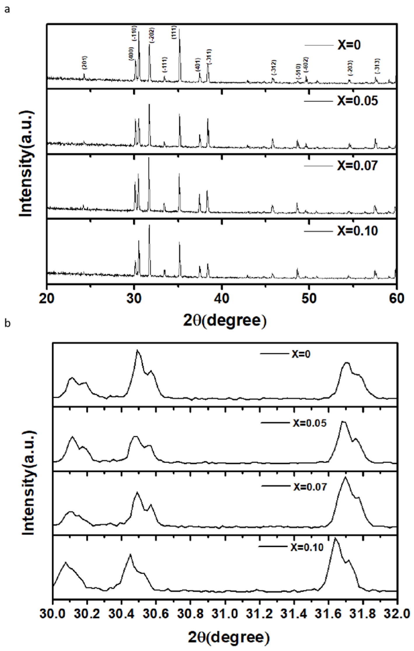
Figure 1a shows the XRD patterns of pure Ga2O3 and Zn-doped Ga2O3 samples. Firstly, the pure Ga2O3 sample exhibits a monoclinic Ga2O3 phase [20]. The peaks are in complete agreement with those of intrinsic Ga2O3 and no impurity peaks are observed in the XRD patterns of the Zn-doped samples, indicating that the Zn-doped samples retain the monoclinic crystal structure of Ga2O3. From the magnified scale of the XRD patterns (Figure 1b), it can be seen that the main diffraction peak positions of the Zn-doped samples shift to lower angles as the Zn concentration increases. This suggests that the lattice parameters gradually increase with the increasing Zn content. On account of the fact that the ionic radius of Zn2+ (0.74 Å) is slightly larger than that of Ga3+ (0.62 Å) [21], the substitution of Ga3+ ions by Zn2+ ions gives rise to an increase in lattice constants and the occurrence of lattice distortion. Therefore, it is indicated that Zn ions are indeed incorporated into the lattices of β-Ga2O3.
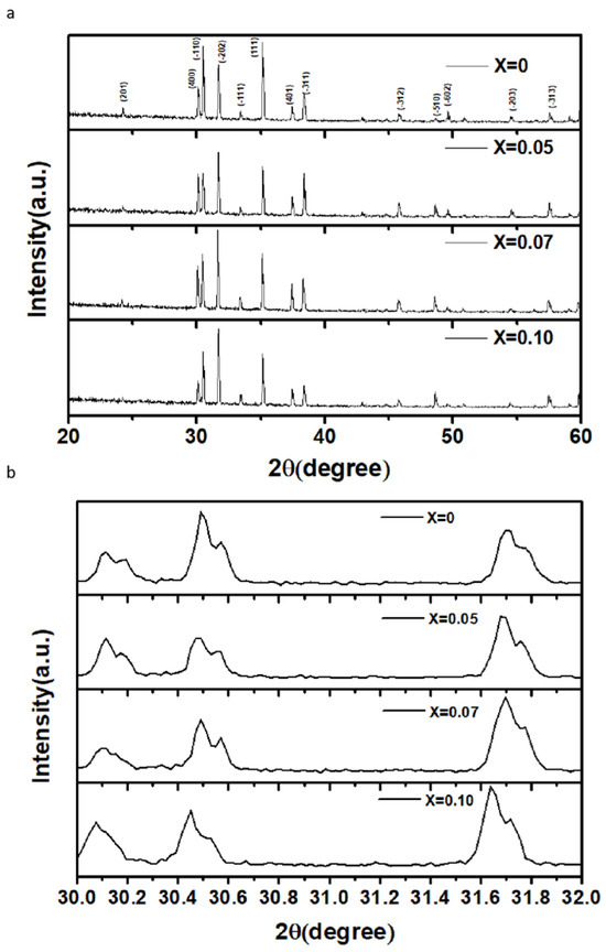
Figure 1.
(a). The XRD patterns of Zn−doped Ga2O3 with different doping concentrations (Ga2−XZnXO3, x = 0, 0.05, 0.07, and 0.1), (b). The partially magnified XRD patterns of Zn−doped Ga2O3 with different doping concentrations (Ga2−XZnXO3, x = 0, 0.05, 0.07, and 0.1).
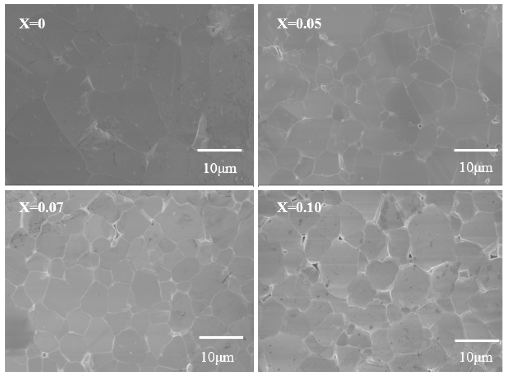
Figure 2 shows the surface morphology images of Ga2O3 doped with different concentrations of Zn. All samples exhibit a dense structure with uniform grain size. After Zn doping, the morphology of the sample grains changes little, but the grain size greatly decreases. This indicates that the incorporation of Zn may increase the crystal growth energy of Ga2O3, inhibiting grain growth and resulting in a microstructure with smaller grains.
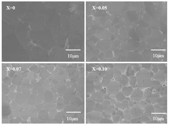
Figure 2.
SEM Images of Zn-doped Ga2O3 of different doping concentrations (Ga2−XZnXO3, x = 0, 0.05, 0.07, and 0.1).
2.2. The Influence of Zn Doping on the Phonon Vibrations of β-Ga2O3
As is well known, the primitive unit cell of β-Ga2O3 contains four Ga atoms and six O atoms, forming two tetrahedral (GaIO4) and two octahedral (GaIIO6) structures. Through analysis based on the C2/m space group, usually, there are 27 optical phonon modes at the Γ point [22]:
Among these, the and modes are Raman-active, while the and modes are infrared-active. The Raman spectra of the pure Ga2O3 and Zn-doped Ga2O3 polycrystalline samples are shown in Figure 3.
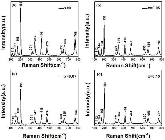
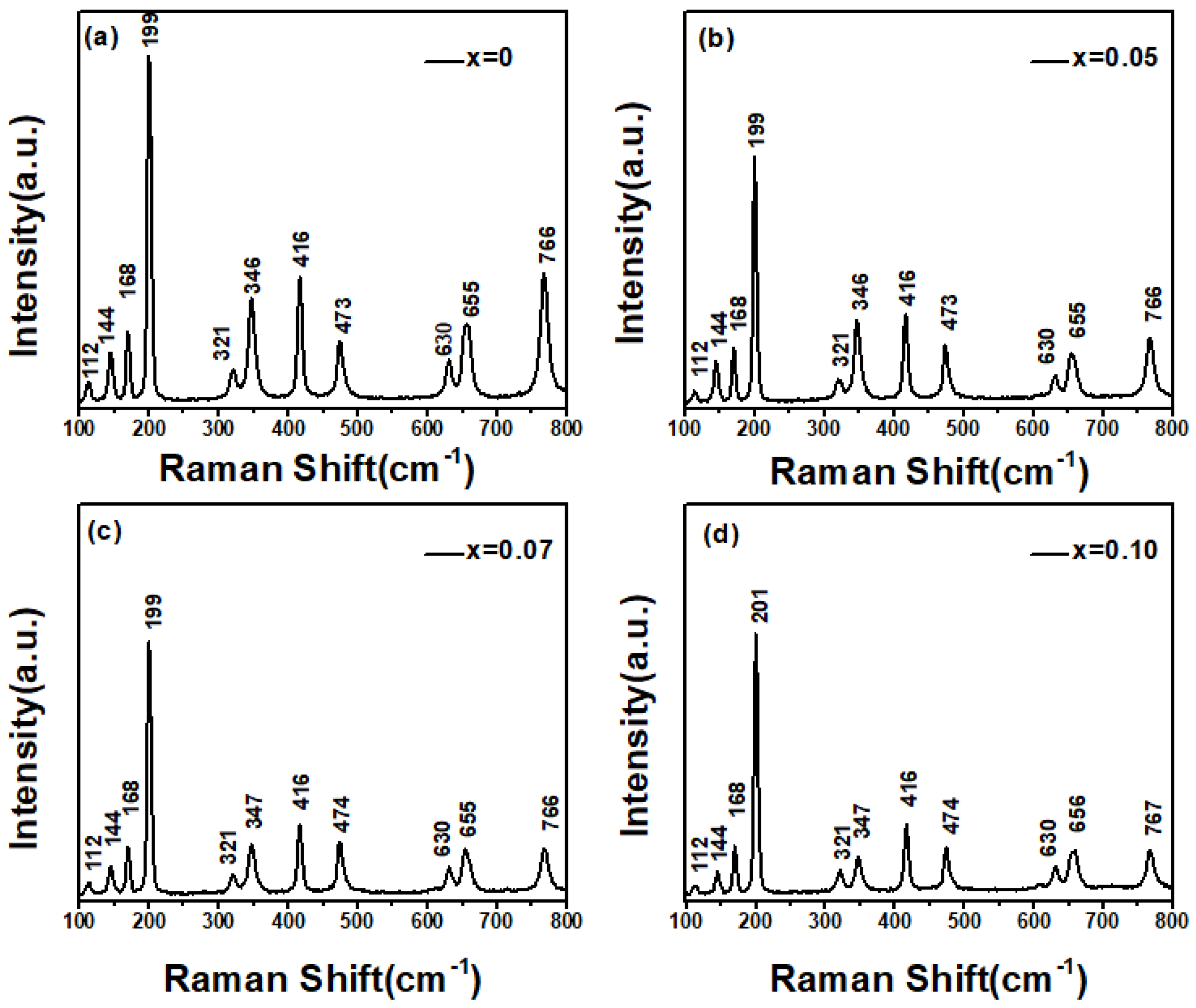
Figure 3.
Raman Spectroscopy of Zn−doped Ga2O3 of different doping concentrations, (a) Ga2O3, (b) Ga1.95Zn0.05O3, (c) Ga1.93Zn0.07O3, (d) Ga1.9Zn0.1O3.
Overall, the Raman spectra of both pure and Zn-doped Ga2O3 samples exhibit 10 Ag modes: (1) at 112 cm−1, (2) at 168 cm−1, (3) at 199 cm−1, (4) at 321 cm−1, (5) at 346 cm−1, (6) at 416 cm−1, (7) at 473 cm−1, (8) at 630 cm−1, (9) at 655 cm−1, and (10) at 766 cm−1, as well as one (2) mode at 144cm−1. These 11 Raman peaks are in complete agreement with the typical Raman peak positions of monoclinic Ga2O3 reported in the literature [22]. Comparing the Raman spectra of pure Ga2O3 with Zn-doped samples, the samples retain a monoclinic structure, which is consist with the XRD results. Most of the Raman peak positions do not show considerable shifts. However, when the doping concentration approaches 10 mol%, the doped sample shows a 2 cm−1 blue shift of the Raman peak (201 cm−1) relative to the corresponding peak of the pure sample at 199 cm−1. The Raman peak at 201 cm−1 is a typical Ga-O chain vibration mode. Due to the doping of Zn, Zn atoms replace some Ga atoms to form ZnGa, which disrupts the Ga-O bonds and alters their vibrational modes, resulting in a blue shift of the peak position.
2.3. The Impact of Zn Doping on the Fundamental Optical Properties of β-Ga2O3
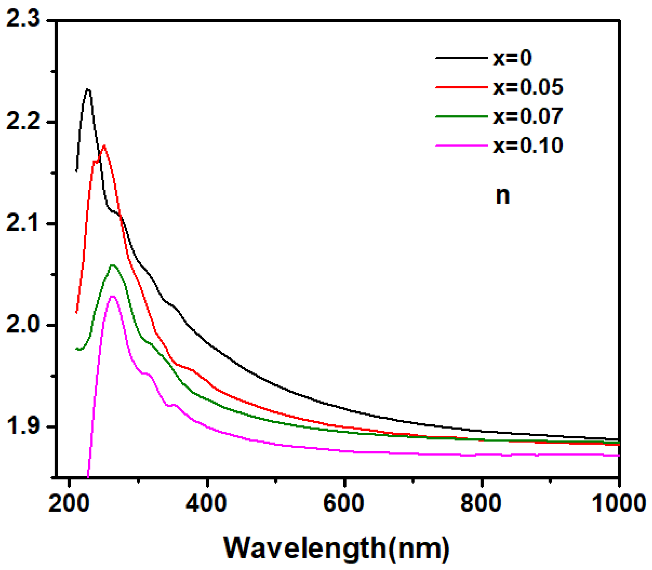
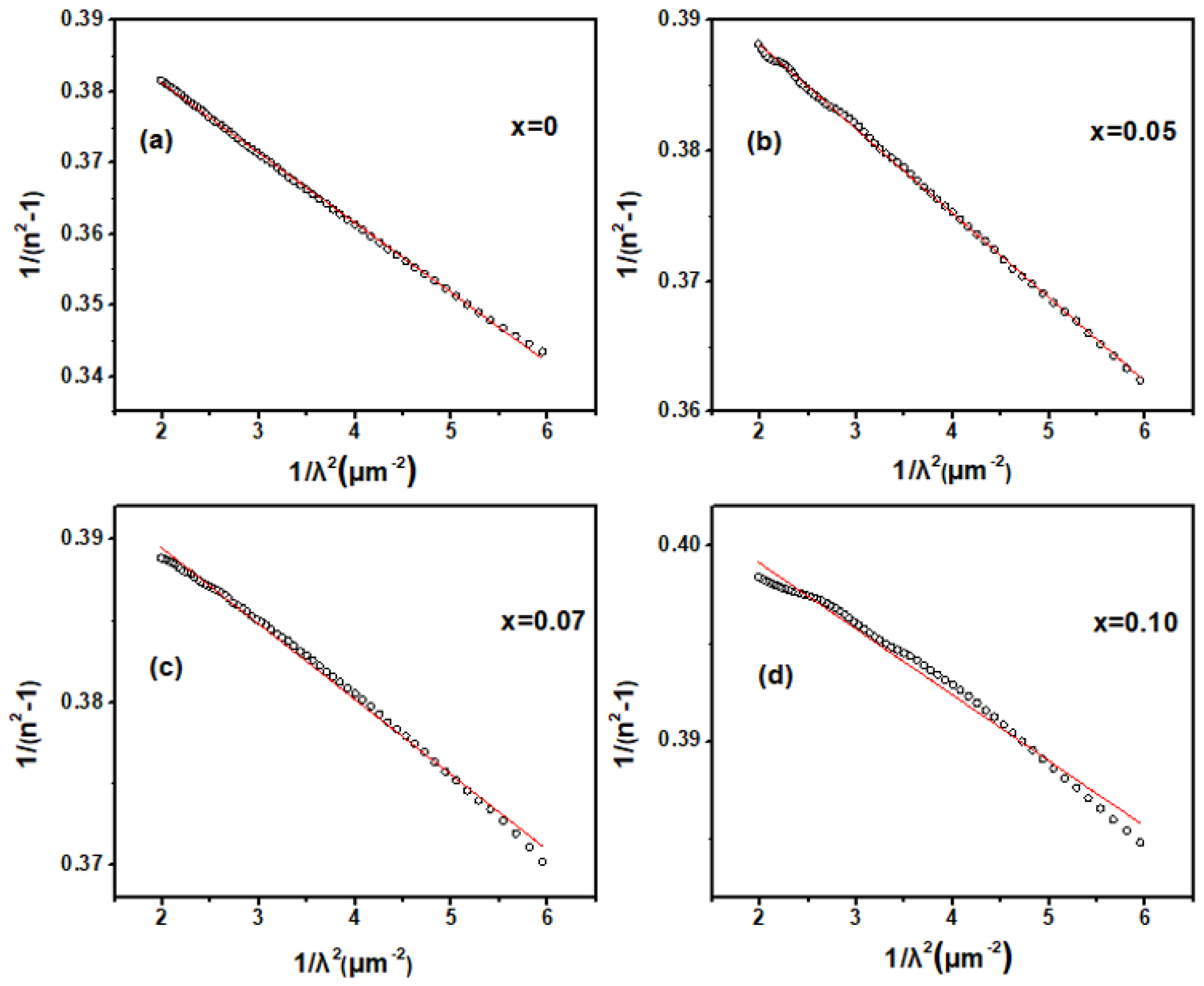
To investigate the effect of Zn doping on the fundamental optical constants and optical bandgap of Ga2O3, spectroscopic ellipsometry (SE) measurements were performed on both pure and doped samples. The refractive index (n) obtained from SE as a function of the wavelength of the incident light in pure and Zn-doped Ga2O3 are showed in Figure 4. From the near-infrared to the visible light region, the refractive index gradually increases as the wavelength of the incident photons decreases; this indicates that it may be transparent for Zn-doped Ga2O3 polycrystalline samples this wavelength range. Generally, in the transparent region, the dispersion behavior can be depicted by the single oscillator Sellmeier model [23]:
where λ0 is the average oscillator position and S0 is the average oscillator strength. The refractive index n of the Zn-doped samples in the transparent region was well-fitted by a single-oscillator Sellmeier relationship, as shown in Figure 5, confirming that this region is transparent for Zn-doped Ga2O3 polycrystalline samples. As the wavelength of the incident photons further decreases into the ultraviolet region, the refractive index n rapidly increases and exhibits a distinct peak. This indicates that the Zn-doped Ga2O3 polycrystalline samples begin to absorb the incident light in this range, entering the weak or intrinsic absorption region. As usual, the peak in the refractive index n may be assigned to the transitions between the critical points (CP) [24]. The peaks of the refractive index n for the intrinsic and Zn-doped samples are located at 220, 250, 260, and 265 nm, respectively, suggesting that the critical point transition energy decreases with increasing doping concentrations. Given that the value of photon energy corresponding to the peaks of n is about 4–5 eV, which is in the range of the value of Ga2O3 band gap (4–5 eV), this CP point thus may be associated with the interband transition between the valence and conduction bands of Ga2O3. This suggests that the optical band-gap would shrink with increases in the Zn doping concentration.
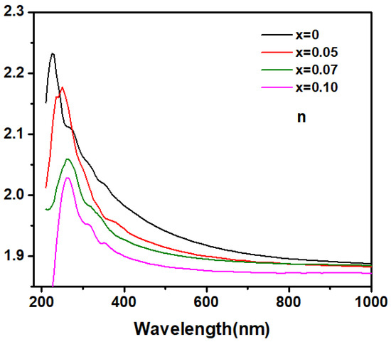
Figure 4.
The relationship between the incident light wavelength and the refractive index n of Zn−doped Ga2O3 with different doping concentrations (Ga2−XZnXO3, x = 0, 0.05, 0.07, and 0.1).
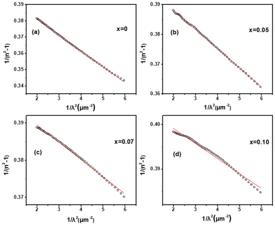
Figure 5.
Dependence of 1/λ2 and 1/(n2−1) in Zn−doped Ga2O3 with different doping concentrations. (Ga2−XZnXO3, x = 0, 0.05, 0.07, and 0.1 (a–d). The circular scatter points represent the actual data, and the red line represents the fitted values.).
To determine the optical bandgap of the samples, in terms of the formula α = 4πkλ, the absorption coefficient α can be obtained from the extinction coefficient k, which is derived from SE. According to the Tauc relationship [12], a fundamental optical absorption rule for semiconductors, the relationship between the optical bandgap Eg and the absorption coefficient α for pure and Zn-doped Ga2O3 polycrystalline materials in the ultraviolet/visible region is given by:
where α is the absorption coefficient, hν is the energy of the incident photons, and A is a material-related constant. For direct bandgap semiconductors, the exponent γ is two, while for indirect bandgap semiconductors, γ is 1/2.
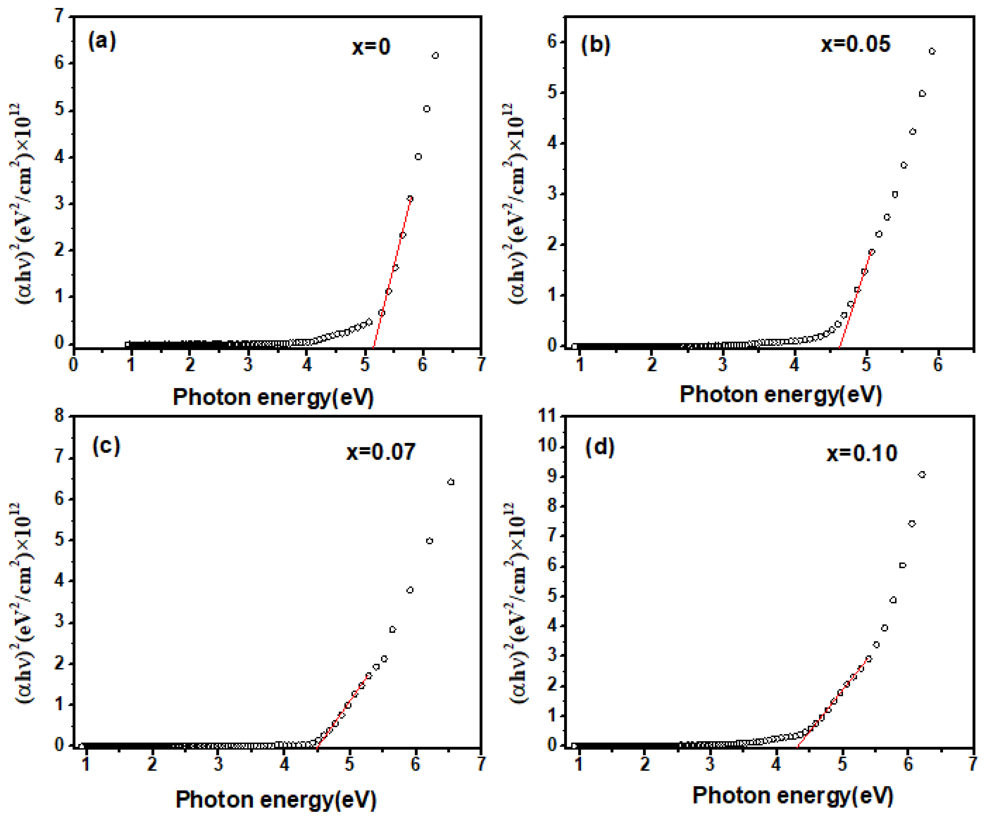
Figure 6 displays the (αhν)2 dependence of the incident photon energy hν in Zn-doped samples, ranging from 0 to 10 mol%. The data were well fitted by the Tauc relationship. It was confirmed that both undoped and Zn-doped Ga2O3 polycrystalline materials remained direct bandgap semiconductors, with optical bandgaps of 5.2 eV, 4.6 eV, 4.5 eV, and 4.4 eV, respectively, which is consistent with the reported values in the literature (near 5 eV) [25]. As the Zn doping concentration increases, the optical bandgap Eg continuously decreased, which is in good agreement with the above evidence. This doping-induced bandgap narrowing phenomenon can be explained by the following two aspects: First-principle calculations indicate that the valence band maximum (VBM) of intrinsic Ga2O3 is formed by the 2p orbitals of oxygen (O), while the conduction band minimum (CBM) is formed by the 4s orbitals of gallium (Ga) [17]. When Zn ions are incorporated into Ga2O3 and replace Ga ions, the 2p orbitals of O in the VBM hybridize with the 3d orbitals of Zn, leading to p-d hybridization. This results in an overlap between the O 2p orbitals and Zn 3d orbitals, causing an upward shift in the energy of the VBM, while the CBM remains formed by the Ga 4s orbitals [25]. Consequently, part of the bandgap is constituted by the hybridized O 2p and Zn 3d orbitals and the Ga 4s orbitals [17,26]. Therefore, as the Zn doping concentration increases, the bandgap tends to shrink. Secondly, in the case of doping, particularly heavy doping, the random distribution of dopant ions can form band tails, resulting in band renormalization effects [26]. As the Zn doping concentration increases, the band tails and impurity bands expand, causing them to overlap and effectively narrowing the width of the intrinsic bandgap. It also contributes to reductions in the optical bandgap.
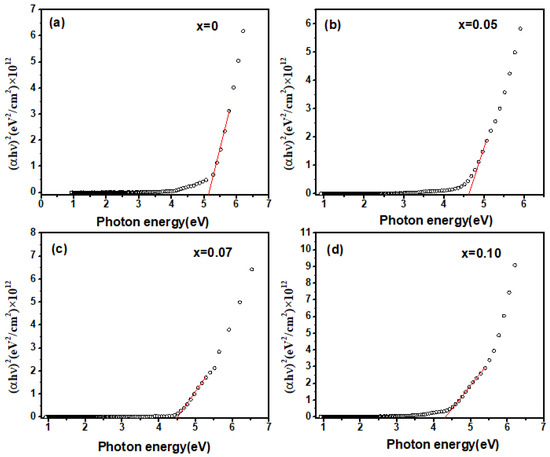
Figure 6.
(αhν)2 as a function of the incident photon energy in Zn−doped Ga2O3, (a) Ga2O3, (b) Ga1.95Zn0.05O3, (c) Ga1.93Zn0.07O3, (d) Ga1.9Zn0.1O3.
2.4. The Influence of Zn Doping on the Photoluminescence Properties of β-Ga2O3
Figure 7 presents the room-temperature PL spectra of Zn-doped Ga2O3 polycrystalline samples under excitation by a 325 nm laser. The PL spectrum of pure Ga2O3 consists of a broad blue-green emission band (400–600 nm) and a red emission band (620–850 nm). Typically, Ga2O3 exhibits three main emission bands: ultraviolet (UV) emissions, blue-green emissions, and red emissions. Harwig et al. [27] suggested that the UV emission arises from the recombination of electrons trapped at donor oxygen vacancies (VO) with holes in the valence band. In the present case, due to the wavelength limitation of the excitation light, UV emissions were not observed. Broad blue-green emissions, commonly in the range of 350–620 nm, frequently occurred in various Ga2O3 nanomaterials [28,29]. This broad blue-green emission band is typically characteristic of bulk and nano-monocrystalline materials [30], originating from the recombination of donor–acceptor defect pairs. Under laser excitation, electrons in the valence band are excited to donor levels, and their subsequent relaxation leads to recombination with holes at acceptor levels, resulting in luminescence. The primary donor defects are oxygen vacancies (VO), while the acceptors are gallium vacancies (VGa) or gallium–oxygen vacancy pairs (VO-VGa) [31]. Therefore, the blue-green emission originates from the recombination of electrons at donor levels (VO) and holes at acceptor levels (VGa or VO-VGa). From Figure 7, it is also evident that, compared to pure Ga2O3, Zn doping considerably enhances the intensity of the blue-green emission in Ga2O3, but the emission peak position does not show an apparent shift. Divalent Zn ions act as acceptor dopants when the substitute trivalent Ga ions. To maintain electrical neutrality, the system tends to generate doubly charged oxygen vacancies for compensation. This process can be described by:
Thus, Zn doping increases the concentration of donor oxygen vacancies (VO) compared to undoped cases, and the concentration of acceptor VO-VGa pairs also increases, giving rise to the enhancement of blue-green emissions.

Figure 7.
The PL spectrum (range from near−infrared to near-ultraviolet) of Zn−doped Ga2O3 with different doping concentration (Ga2−XZnXO3, x = 0, 0.05 and 0.1).
Figure 7.
The PL spectrum (range from near−infrared to near-ultraviolet) of Zn−doped Ga2O3 with different doping concentration (Ga2−XZnXO3, x = 0, 0.05 and 0.1).
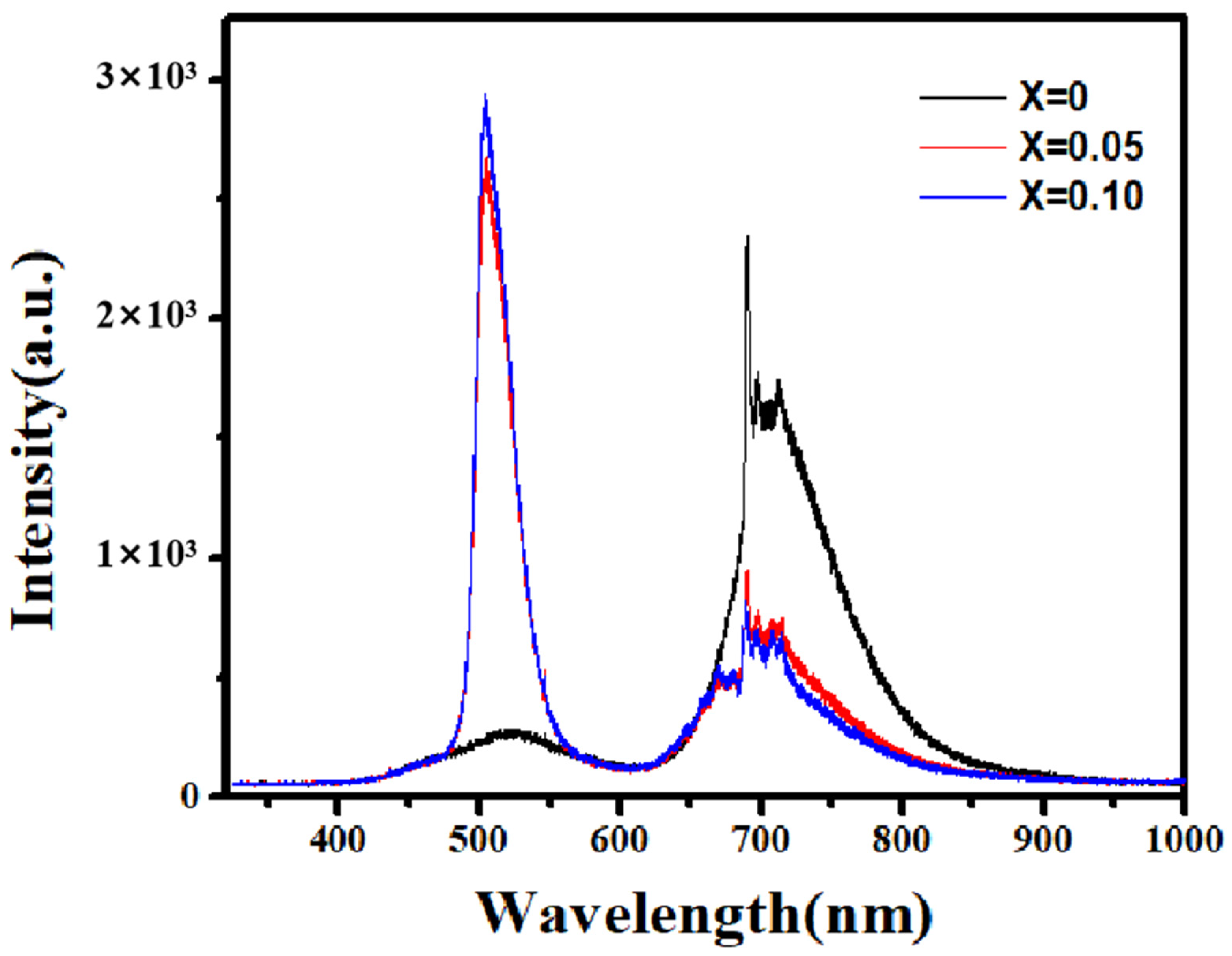
As for the red emission in the PL spectrum of Ga2O3 polycrystals, a sharp and continuous red emission is observed in the 690–750 nm range in Figure 7, indicating the transitions between discrete energy levels [32,33]. The mechanism behind this red emission in Ga2O3 still remains uncertain and is highly debated. The previous literature has reported that red emissions often appear in Li-, Cr-, and Fe-doped Ga2O3 [34,35,36,37], originating from intra-transitions of outer orbital electrons of the doped ions. However, in the present case, the pure Ga2O3 oxide was not doped with such ions, so what causes the red emission? Related reports indicate that red emissions also exist in other forms of pure Ga2O3 oxides. For example, Ma et al. prepared pure Ga2O3 nanorods using a hydrothermal method and obtained a PL spectra almost identical to those seen in this case [38]. We note that N doping can also induce red emissions in Ga2O3, and the high-temperature calcination of Ga2O3 in an air atmosphere inevitably introduces trace amounts of N, which may be the cause of the red emission in the samples. T. Zhang et al. also observed sharp and continuous red emissions (690–750 nm) in pure Ga2O3 samples prepared at high temperatures and attributed it to trace nitrogen (N) introduced during the high-temperature (1350 °C) preparation process [39]. Here, Zn doping causes a noticeable reduction in the red emission of Ga2O3. This may be due to the Zn doping suppressing the introduction of N, which causes the weakening of red emissions. T. Zhang et al. also observed a reduction in red emissions in Ge-doped Ga2O3 [40].
3. Materials and Methods
A series of polycrystalline samples of Ga2−XZnXO3 (x = 0, 0.05, 0.07, and 0.1) were synthesized by a solid-state reaction. The mixtures of ZnO (99.99%) and Ga2O3 (99.99%) with a stoichiometric ratio were ball-milled in deionized water for 8 h. The dried powders were pressed into the pellets. The pressed pellets were calcinated at 1050 °C for 10 h in air, then crushed and ball-milled again for 8 h, and finally sintered at 1500 °C in air for 6 h. After sintering, the samples’ surfaces were polished to achieve the desired smooth surface for subsequent crystalline structure, microstructure, and optical characterizations. The crystalline structure of the samples was checked by x-ray diffraction (D8 Discover X Series 2, Bruker Co., Beijing, China). The microstructure of the samples was observed by scanning electron microscopy (JSM7500SF, JEOL, Tokyo, Japan). The structural and phonon vibration characteristics of the samples were characterized using laser Raman spectroscopy (Renishaw inVia, Shanghai, China). Spectroscopic ellipsometry (V-VASE, J.A. Woollam, Lincoln, NE, USA) was employed to obtain the fundamental optical constants and band-gap width of the Ga2O3 polycrystalline samples. Photoluminescence (PL) spectroscopy was performed by a fluorescence spectrometer (Lab RAM HR 800UV, Horiba Jobin-Yvon, Paris, France) with a 325 nm laser excitation source.
4. Conclusions
In summary, the effects of Zn doping on the optical properties of Ga2O3 crystals are revealed. For Zn-doped Ga2O3, the introduced Zn ions disrupted the Ga-O bonds, altering the Ga-O vibration modes and causing a blue shift at the related Raman mode. The near-infrared and visible light spectrum lied within the transparent region. The fundamental optical bandgap decreased with increasing Zn doping concentrations. The shrinkage of the optical bandgap of the doped samples was due to the p-d orbital hybridization of the O 2p and Zn 3d orbitals, and the band renormalization effects induced band-tails. The blue-green luminescence came from the recombination of electrons at donor levels (VO) and holes at acceptor levels (VGa or VO-VGa). Zn doping increased the concentration of oxygen vacancies (VO), leading to a great enhancement in the blue-green luminescence intensity of Ga2O3. However, Zn doping resulted in a noticeable reduction in the red luminescence of Ga2O3, which may be attributed to the Zn doping suppressing nitrogen incorporation from the air during high-temperature preparation processes.
Author Contributions
Investigation, Y.Y. and S.Z.; Writing—original draft, Y.Y.; Writing—review & editing, W.B. and Y.Z.; Supervision, J.Y. and X.T.; Project administration, X.T. All authors have read and agreed to the published version of the manuscript.
Funding
The work is supported by the Natural Science Foundation of Chongqing (CSTB2022NSCQMSX0589 and CSTB2022NSCQ-MSX1474), the National Science Foundation of China (61574058 and 61674058), and the ECNU (East China Normal University) Multifunctional Platform for Innovation (006).
Institutional Review Board Statement
Not applicable.
Informed Consent Statement
Not applicable.
Data Availability Statement
Data are contained within the article.
Conflicts of Interest
The authors declare no conflicts of interest.
Abbreviations
The following abbreviations are used in this manuscript:
| Vo/VGa | Vacancy of Oxygen/Gallium |
| PL | Photoluminescence |
| MOCVD | Metal-organic Chemical Vapor Deposition |
| XRD | X-Ray Diffraction |
| SEM | Scan Electron Microscope |
| SE | Spectroscopic Ellipsometry |
| CP | Critical Points |
| CBM | Conduction Band Minimum |
| VBM | Valence Band Maximum |
| UV | Ultra-violet |
References
- Roy, R.; Hill, V.G.; Osborn, E.F. Polymorphism of Ga2O3 and the System Ga2O3-H2O. J. Am. Chem. Soc. 1952, 74, 719–722. [Google Scholar]
- Playford, H.Y.; Hannon, A.C.; Barney, E.R.; Walton, R.I. Structures of Uncharacterised Polymorphs of Gallium Oxide from Total Neutron Diffraction. Chem. A Eur. J. 2013, 19, 2803–2813. [Google Scholar]
- Yoshioka, S.; Hayashi, H.; Kuwabara, A.; Oba, F.; Matsunaga, K.; Tanaka, I. Structures and energetics of Ga2O3 polymorphs. J. Phys. Condens. Matter 2007, 19, 346211. [Google Scholar]
- Guo, D.Y.; Li, P.G.; Chen, Z.W.; Wu, Z.P.; Tang, W.H. Research Progress on Ultra-Wide Bandgap Semiconductor β-Ga2O3, Deep Ultraviolet Transparent Electrodes, and Solar-Blind Detectors. Acta Phys. Sin. 2019, 68, 7–42. [Google Scholar] [CrossRef]
- Higashiwaki, M.; Sasaki, K.; Murakami, H.; Kumagai, Y.; Koukitu, A.; Kuramata, A.; Masui, T.; Yamakoshi, S. Recent progress in Ga2O3 power devices. Semicond. Sci. Technol. 2016, 31, 034001. [Google Scholar] [CrossRef]
- Liu, Z.; Yamazaki, T.; Shen, Y.; Kikuta, T.; Nakatani, N.; Li, Y. O2 and CO sensing of Ga2O3 multiple nanowire gas sensors. Sens. Actuators B Chem. 2008, 129, 666–670. [Google Scholar]
- Ji, Z.; Du, J.; Fan, J.; Wang, W. Gallium oxide films for filter and solar-blind UV detector. Opt. Mater. 2006, 28, 415–417. [Google Scholar]
- Yu, F.-P.; Ou, S.-L.; Wuu, D.-S. Pulsed laser deposition of gallium oxide films for high performance solar-blind photodetectors. Opt. Mater. Express 2015, 5, 1240–1249. [Google Scholar]
- Li, Z.; Xu, Y.; Zhang, J.; Cheng, Y.; Chen, D.; Feng, Q.; Xu, S.; Zhang, Y.; Zhang, J.; Hao, Y.; et al. Flexible Solar-Blind Ga2O3 Ultraviolet Photodetectors with High Responsivity and Photo-to-Dark Current Ratio. IEEE Photonics J. 2019, 11, 1–9. [Google Scholar]
- Wang, H.; Zhou, Q.; Liang, S.; Wen, R. Fabrication and Characterization of AlGaN-Based UV LEDs with a ITO/Ga2O3/Ag/Ga2O3 Transparent Conductive Electrode. Nanomaterials 2019, 9, 66. [Google Scholar] [CrossRef]
- Minami, T.; Nishi, Y.; Miyata, T. Effect of the thin Ga2O3 layer in n+-ZnO/n-Ga2O3/p-Cu2O heterojunction solar cells. Thin Solid Films 2013, 549, 65–69. [Google Scholar] [CrossRef]
- Du, X.; Li, Z.; Luan, C.; Wang, W.; Wang, M.; Feng, X.; Xiao, H.; Ma, J. Preparation and characterization of Sn-doped beta-Ga2O3 homoepitaxial films by MOCVD. J. Mater. Sci. 2015, 50, 3252–3257. [Google Scholar] [CrossRef]
- Leedy, K.D.; Chabak, K.D.; Vasilyev, V.; Look, D.C.; Boeckl, J.J.; Brown, J.L.; Tetlak, S.E.; Green, A.J.; Moser, N.A.; Crespo, A.; et al. Highly conductive homoepitaxial Si-doped Ga2O3 films on (010) β-Ga2O3 by pulsed laser deposition. Appl. Phys. Lett. 2017, 111, 012103. [Google Scholar]
- Zhang, F.B.; Saito, K.; Tanaka, T.; Nishio, M.; Guo, Q.X. Electrical properties of Si doped Ga2O3 films grown by pulsed laser deposition. J. Mater. Sci. Mater. Electron. 2015, 26, 9624–9629. [Google Scholar] [CrossRef]
- Feng, Z.; Bhuiyan, A.F.M.; Kalarickal, N.K.; Rajan, S.; Zhao, H. Mg acceptor doping in MOCVD(010) β-Ga2O3. Appl. Phys. Lett. 2020, 117, 222106. [Google Scholar]
- Pearton, S.J.; Yang, J.; Cary, P.H.; Ren, F.; Kim, J.; Tadjer, M.J.; Mastro, M.A. A review of Ga2O3 materials, processing, and devices. Appl. Phys. Rev. 2018, 5, 01130. [Google Scholar] [CrossRef]
- Li, C.; Yan, J.-L.; Zhang, L.-Y.; Zhao, G. Electronic structures and optical properties of Zn-doped β-Ga2O3 with different doping sites. Chin. Phys. B 2012, 21, 127104. [Google Scholar]
- Feng, X.J.; Li, Z.; Mi, W.; Luo, Y.; Ma, J. Mg-doped beta-Ga2O3 films with tunable optical band gap prepared on MgO(110) substrates by metal-organic chemical vapor deposition. Mater. Sci. Semicond. Process. 2015, 34, 52–55. [Google Scholar] [CrossRef]
- Vasyltsiv, V.; Kostyk, L.; Tsvetkova, O.; Lys, R.; Kushlyk, M.; Pavlyk, B.; Luchechko, A. Luminescence and Conductivity of β-Ga2O3 and β-Ga2O3:Mg Single Crystals. Acta Phys. Pol. A 2021, 142, 132–138. [Google Scholar] [CrossRef]
- Geller, S. Crystal Structure of β-Ga2O3. J. Chem. Phys. 1960, 33, 676–684. [Google Scholar] [CrossRef]
- Wang, X.H.; Zhang, F.B.; Saito, K.; Tanaka, T.; Nishio, M.; Guo, Q.X. Electrical properties and emission mechanisms of Zn-doped β-Ga2O3 films. J. Phys. Chem. Solids 2014, 75, 1201–1204. [Google Scholar] [CrossRef]
- Dohy, D.; Lucazeau, G.; Revcolevschi, A. Raman spectra and valence force field of single-crystalline β-Ga2O3. J. Solid State Chem. 1982, 45, 180–192. [Google Scholar] [CrossRef]
- Drdomenico, M.; Wemple, S.H. Oxygen-Octahedra Ferroelectrics. I. Theory of Electro-optical and Nonlinear optical Effects. J. Appl. Phys. 1969, 40, 720–734. [Google Scholar]
- Hu, Z.G.; Li, Y.W.; Zhu, M.; Zhu, Z.Q.; Chu, J.H. Composition dependence of dielectric function in ferroelectric BaCoxTi1−xO3 films grown on quartz substrates by transmittance spectra. Appl. Phys. Lett. 2008, 92, 081904. [Google Scholar]
- Ueda, N.; Hosono, H.; Waseda, R.; Kawazoe, H. Anisotropy of electrical and optical properties in β-Ga2O3 single crystals. Appl. Phys. Lett. 1997, 71, 933–935. [Google Scholar]
- Guo, Y.; Yan, H.; Song, Q.; Chen, Y.; Guo, S. Electronic structure and magnetic interactions in Zn-doped beta-Ga2O3 from first-principles calculations. Comput. Mater. Sci. 2014, 87, 198–201. [Google Scholar]
- Harwig, T.; Kellendonk, F.; Slappendel, S. The ultraviolet luminescence of β-galliumsesquioxide. J. Phys. Chem. Solids 1978, 39, 675–680. [Google Scholar] [CrossRef]
- Yan, S.; Wan, L.; Li, Z.; Zhou, Y.; Zou, Z. Synthesis of a mesoporous single crystal Ga2O3 nanoplate with improved photoluminescence and high sensitivity in detecting CO. Chem. Commun. 2010, 46, 6388–6390. [Google Scholar]
- Yang, H.; Shi, R.; Yu, J.; Liu, R.; Zhang, R.; Zhao, H.; Zhang, L.; Zheng, H. Single-Crystalline β-Ga2O3 Hexagonal Nanodisks: Synthesis, Growth Mechanism, and Photocatalytic Activities. J. Phys. Chem. C 2009, 113, 21548–21554. [Google Scholar]
- Nogales, E.; Méndez, B.; Piqueras, J. Cathodoluminescence from β-Ga2O3 nanowires. Appl. Phys. Lett. 2005, 86, 113112. [Google Scholar]
- Binet, L.; Gourier, D. Origin of the blue luminescence of β-Ga2O3. J. Phys. Chem. Solids 1998, 59, 1241–1249. [Google Scholar] [CrossRef]
- Vanithakumari, S.C.; Nanda, K.K. A One-Step Method for the Growth of Ga2O3-Nanorod-Based White-Light-Emitting Phosphors. Adv. Mater. 2009, 21, 3581–3584. [Google Scholar] [CrossRef]
- Sawada, K.; Adachi, S. Photoluminescence Properties of Eu3+ in Ga2O3-Tb3Ga5O12:Cr3+ Phosphor Synthesized by Metal Organic Deposition. ECS J. Solid State Sci. Technol. 2014, 3, R238–R244. [Google Scholar] [CrossRef]
- Jiang, J.; Zhang, J. Temperature-resolved photoluminescence, Raman and electrical properties of Li doped Ga2O3 nanostructure. Ceram. Int. 2020, 46, 2409–2412. [Google Scholar] [CrossRef]
- Jiang, J.; Zhang, J.; Li, J.; Xu, D. Red-light emission of Li-doped Ga2O3 one-dimensional nanostructures and the luminescence mechanism. Chem. Phys. Lett. 2019, 719, 8–11. [Google Scholar] [CrossRef]
- Nogales, E.; García, J.A.; Méndez, B.; Piqueras, J. Red luminescence of Cr in β-Ga2O3 nanowires. J. Appl. Phys. 2007, 101, 033517. [Google Scholar] [CrossRef]
- Sun, R.; Ooi, Y.K.; Dickens, P.T.; Lynn, K.G.; Scarpulla, M.A. On the origin of red luminescence from iron-doped β-Ga2O3 bulk crystals. Appl. Phys. Lett. 2020, 117, 052101. [Google Scholar] [CrossRef]
- Ma, T.Y.; Kong, C.Y.; Li, W.J.; He, X.W.; Hu, H.; Huang, L.J.; Zhang, H.; Xiong, Y.Q.; Li, H.L.; Ye, L.J.; et al. Size regulation and photoluminescence properties of β-Ga2O3 nanomaterials. Acta Phys. Sin. 2020, 069, 246–256. [Google Scholar] [CrossRef]
- Zhang, T.; Lin, J.; Zhang, X.; Huang, Y.; Xu, X.; Xue, Y.; Zou, J.; Tang, C. Single-crystalline spherical β-Ga2O3 particles: Synthesis, N-doping and photoluminescence properties. J. Lumin. 2013, 140, 30–37. [Google Scholar] [CrossRef]
- Zhang, T.T. Controlled Synthesis, Doping and Luminescence Properties of Low-Dimensional Ga2O3 Nanomaterials. Master’s Thesis, Hebei University of Technology, Tianjin, China, 2013. [Google Scholar]
Disclaimer/Publisher’s Note: The statements, opinions and data contained in all publications are solely those of the individual author(s) and contributor(s) and not of MDPI and/or the editor(s). MDPI and/or the editor(s) disclaim responsibility for any injury to people or property resulting from any ideas, methods, instructions or products referred to in the content. |
© 2025 by the authors. Licensee MDPI, Basel, Switzerland. This article is an open access article distributed under the terms and conditions of the Creative Commons Attribution (CC BY) license (https://creativecommons.org/licenses/by/4.0/).