Abstract
The interest in ultrathin silver (Ag) films has increased due to their high surface plasmon resonance for coatings of only a few nm. Low roughness ultrathin films of 1 to 9 nm have been deposited on different substrates, such as polyethylene terephthalate (PET) and optical glass, using radio frequency (RF) magnetron sputtering. Films show good surface plasmon resonance up to 7 nm thickness, as revealed by the ultraviolet-visible (UV-Vis) spectra. The roughness of the films, investigated by Atomic Force Microscopy (AFM) and Scanning Electron Microscopy (SEM), is small, and one can conclude that depositions are smooth and homogeneous. The bandgap values decrease with film thickness. The refractive index of the films, calculated from ellipsometry measurements, leads to values of under 1 visible domain, with minima in the wavelength range of 400–600 nm. The results are useful for obtaining lower roughness ultrathin Ag films with good surface plasmon resonance for photonic applications.
1. Introduction
Thin metal films, especially of Au, Ag, and Cu, have recently attracted scientific and technological interest due to their interesting applications for perfect lenses, optical cloaking devices [1], surface-enhanced Raman scattering (SERS) [2], transparent conductive coatings, transparent electrodes for “smart windows” and solar cells, catalytic coatings, surface plasmon resonance (SPR) based biosensors [3], antibacterial coatings [4], etc.
Silver, as a thin film under 20 nm thickness, possesses high optical properties with excellent performance in optical applications and presents a significant difference compared to bulk material [3]. A thin film of silver is partially transparent and conductive at the same time [5] and is the most common plasmonic material [3]. Silver (Ag) is known as potentially the best plasmonic material, with the naturally lowest ohmic losses at optical frequencies [6]. Silver has the best optical and electrical properties and better performances compared to other metal films in optical devices [7]. Silver nanoparticle deposition is very reproducible because the silver nanoparticle size distribution under identical deposition conditions is similar, which recommends it for industrial applications [8]. However, the development of silver-based materials for plasmonic and metamaterials is limited due to some technological challenges in thin film synthesis, nanoscale fabrication techniques [6], and metal layer growth morphology [9].
Several techniques are used for Ag thin film deposition, such as glancing angle deposition (GLAD) [1], plasma enhanced atomic layer deposition (PEALD) [2], alternating current (AC) magnetron sputtering [3], thermal evaporation and low-pressure direct current (DC) plasma sputtering [5], DC magnetron sputtering [4,7], pulsed laser deposition (PLD) [7], RF magnetron sputtering [10], or electron beam evaporation [5]. Thermal evaporation methods have major disadvantages, such as poor adherence and stability of films. GLAD and PEALD can be used for special patterns. The magnetron sputtering method is one of the best choices for obtaining homogeneous and controlled ultrathin films of Ag.
Plasmonics and nano-plasmonics refer to the generation, detection, and driving of signals at optical frequencies along metal-dielectric interfaces at the nanometer scale. Like photonics, plasmonics is applied to miniaturizing enhanced optical devices: optical sensing, metal-dielectric-metal versatile nanostructures, or energy harvesting cells. Surface Plasmon Resonance (SPR) measurements can be used to detect molecular adsorption in biopolymers; a shift in this resonance due to a change in the local index of refraction upon adsorption on nanoparticles can be useful to identify biopolymers [11].
The complete understanding of the optical characteristics of ultrathin silver films (under 10 nm thickness) integrated into photonic structures is rather approximate and difficult to be practically understood, despite the obvious simplicity of a single ultrathin film deposition by the magnetron sputtering method. In order to prepare ultra-thin layers for different applications, it is important to understand how to deposit Ag on various substrates without a seed layer. Commercial substrates like optical glass and oxide films, plastics like PET, or other polymers are studied worldwide, and recent papers have attempted to understand the problems linked to ultra-thin Au or Ag films deposition and properties [11,12]. Colin et al. [13] reviewed the monitoring of ultra-thin metal film growth by comparing several deposition methods and optical and electrical properties but did not indicate a low-power method of deposition. Grachev et al. [14] also presented a real-time monitoring of film growth, but they used relatively high power, around 50 W, for the magnetron sputtering deposition.
The reason for this work is to use low power of 1 W in selected working conditions, for low roughness deposition, by magnetron sputtering, of ultrathin films of Ag of 1–9 nm thickness on various substrates, namely, optical glass (OG), and thin and thick PET and to study the structure and properties of the obtained new nanostructures. Decreasing the thickness of the continuous Ag layer as much as possible is important for all optical and electronic devices and especially for flexible components. The author’s intention was to find for the low-power magnetron sputtering deposition method, the proper working conditions without a special cooling stage in order to find a simple and cheap method for such Ag ultrathin depositions. During the growth process, the Ag metal clusters connect with each other to form a continuous structure in long range, which was investigated using SEM. Therefore, to reach the continuous structure at minimum Ag thickness, considering the roughness of commercial substrate materials we used, was a target for us. According to the Ag atomic dimension, we concluded that the best roughness is in the range of 4 to 6 atomic layers, which is about λ/50 in the UV domain and λ/100 in the visible domain. We concluded that the Ag ultra-thin film could be processed using a very low rate of deposition, preferably under 0.02 nm/sec, in vacuum conditions assisted with a pure Argon (99.99%) gas flow of 2 × 10⁻²–3 × 10⁻² L/min. We established the vacuum parameters according to the specificity of the chosen vacuum system. This work tries to find answers to the above-mentioned problems and to make an original study on the influence of substrate and the substrate-film system (considered as a Vis transparent material) properties, highlighting the bandgap variation for these systems.
2. Materials and Methods
The magnetron sputtering depositions were made using a Radio Frequency Magnetron Sputtering VARIAN ER3119 apparatus. The deposition conditions are presented in Table 1. The Ag layer thickness was monitored during the deposition process with the help of a quartz sensor whose sensitivity is 0.1 nm, a sensor that is integrated as a part of the magnetron sputtering equipment. Therefore, the standard deviation for the measurement of the deposition thickness must be 0.05 nm.

Table 1.
Deposition conditions.
The Magnetron Sputtering apparatus used usually works in the RF domain. In our case, by using very low powers of about 1 W, the RF was not reached and there was no problem with heating. The low-power plasma of 1 W was very stable, with no plasma quenching. Under the above deposition conditions, ultrathin films of 1, 3, 5, 7, and 9 nm thickness were deposited on optical glass (BK7 type), thick PET, and thin PET, with the sample codes presented in Table 2. The optical glass substrate roughness was under 1 nm but the substrates of PET, both thin and thick, had some major defects which could not be removed and appeared in some of the AFM and SEM images. The roughness of PET substrates apparently decreases from around 10 nm (PET) and 1.8 nm (PETs), before deposition, to the values indicated in Table 3 (which are lower for both substrates in the case of 1 nm film thickness and lower for all deposition thicknesses in the case of thick PET) after the Ag deposition in Ar plasma. Each substrate was carefully cleaned with ethanol, visually checked, and dried in air before the Ag film deposition. Three different samples were performed for the representative thickness (1, 5, and 9 nm) and only two for the other thicknesses (3 and 7 nm), and the resulting films have identical properties.
Table 2.
Sample codes.
Table 3.
Roughness of ultrathin films deposited on PET, thin PET, and optical glass (SO).
The atomic force microscopy (AFM) system used for investigating the morphology and the state of the surface, together with the quality of depositions in terms of low roughness, was an XE100 model from Park System (Suwon, Republic of Korea). The images were recorded in non-contact mode using commercial silicon tips.
A scanning electron microscope, SEM (FEI QUANTA INSPECT S), FEI Company, Hillsboro, OR, USA, equipped with EDAX was used to observe the structures and morphology of the samples. The FEI Inspect F50 Microscope has an optional beam deceleration mode to get surface and compositional information from conductive samples. The microscope uses a stable high current FEG (field emission gun) up to 30 kV. The images have a 5 μm resolution and ×20,000 magnification.
The transmittance, reflectance, and absorbance were measured with a UV-Vis Lambda 35 (PerkinElmer, Waltham, MA, USA) Spectrophotometer, with the following characteristics: Range 190–1100 nm, Bandwidth 0.5–4 nm (our samples were analyzed with a 1 nm slit), Absorbance range (linearity 0.99 r2) 3.2 A, Working temperature 15 °C, 35 °C, Relative humidity 20%, 80%, Precision 0.1 nm, and Scanning rate 60–2880 nm/min (for our samples—240 nm/min). Since the transmittance and reflectance spectra were performed with the PerkinElmer Lambda 35 spectrophotometer, which is a device with a high degree of reliability, and the calculation of the forbidden band was performed according to the calculation algorithm from the literature with the help of the Origin software, we consider that all measurements are perfectly reproducible, because the transmission spectra are correctly recorded by the PerkinElmer Lambda 35 spectrophotometer. The band gap calculations usually have an error of under 1%.
The refraction index, n, and the extinction coefficient, k, related to the absorption loss were calculated using data collected by ellipsometry using a Spectro-ellipsometer VVASE—Variable Angle Spectroscopic Ellipsometry (Woollam, Lincoln, NE, USA), at 60°, 65°, and 70° incidence angles in the spectral range 250–1700 nm. From the measurement of amplitude ratio Ψ (Y) and phase difference Δ (D) at each wavelength and at different incident angles, optical models were generated by WVASE32 software, and the n and k parameters were measured. WVASE32 is a spectroscopic ellipsometry software from J. A. Woollam Co. that allows building a model based on the sample structure and describing the properties of target materials using different oscillators.
3. Results and Discussion
The samples with 1, 5, and 9 nm thickness of deposited Ag film were chosen as the most representative for the structural and property investigations.
3.1. Atomic Force Microscopy (AFM)
The surface morphology of the films was examined by the AFM method. The scan area for all films was 2 × 2 μm2. Figure 1a–i show AFM images of the as-deposited Ag films on PET, thin PET (PETs), and optical glass (SO) substrate.
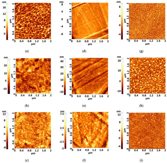
Figure 1.
AFM images of as-deposited ultrathin films (a) PET-Ag1, (b) PET-Ag5, (c) PET-Ag9, (d) PETs--g1, (e) PETs-Ag5, (f) PETs-Ag9, (g) SO-Ag1, (h) SO-Ag5, (i) SO-Ag9.
For the as-deposited films, the surface was crack-free, smooth, and homogeneous, composed of very small aggregates with a maximum height of ca. 9 nm. AFM 2D images of the Ag films show different morphologies of surface, depending on the Ag films’ thickness and substrates, which can be related to the agglomeration of crystallites and defects of PET surface. The most homogeneous films are those deposited on optical glass. The films deposited on thick PET show some wave-like deposition tendency, while films deposited on thin PET present isolated grains. According to the AFM 3D images, the aggregates are pyramidal in all samples. The roughness of the as-deposited films is presented in Table 3.
The surface roughness values shown in Table 3 show that the lowest roughness values are registered in the case of films of 1 and 9 nm thickness deposited on thin PET and optical glass. It is likely that the 9 nm thick Ag film covers the irregularities of the substrates surface compared to 5 nm thick films and this explains the roughness decrease.
Zhang et al. reported that it is very difficult to obtain very thin and smooth Ag films at the same time due to 3D island formation during the film growth [15]. A rough surface morphology will lower the film conductivity and cause more optical loss, even getting nonconductive layers when the islands cannot form percolation paths [15]. The films with a deposition thickness lower than 5 nm present lower roughness than 5 nm in all cases and under 3 or 2 nm in the case of 1 nm deposition thickness, as indicated by the quartz monitor. Unfortunately, because of 3D island formation, a continuous film is not formed and the conductivity threshold is not reached. As shown in Table 3 and Figure 1, the ultrathin films over 5 nm and under 9 nm deposition thickness together present conductivity properties because they are continuous films together with SPR properties. All samples obtained by this low-power deposition method present much lower roughness than the samples reviewed by Colin et al. [13], with a roughness of about 10 nm.
According to the Ag atomic diameter, we concluded that the best roughness is between 4 atomic layers and 6 atomic layers, which is about λ/50 in UV and λ/100 in visible. As presented by Colin et al. [13], the electrical percolation threshold appears at about 7 nm Ag film thickness, which indicates that films of 7 nm and 9 nm present the best electrical conduction properties in a condition of lower roughness than the film of 5 nm. The films of 3 and 1 nm have low roughness, but even if they have SPR properties, as presented in the next chapters, they are not electrically conductive.
3.2. Scanning Electron Microscopy (SEM)
Figure 2a–i show SEM images of Ag films deposited on different substrates with 1, 5, and 9 nm thickness. The images confirm the fact that the depositions are homogeneous and smooth. Some cracks appeared in the film of 1 nm deposited on PET, both thin and thick.
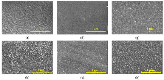
Figure 2.
SEM images of as-deposited ultrathin films:(a) PET-Ag1, (b) PET-Ag5, (c) PET-Ag9, (d) PETs-Ag1, (e) PETs-Ag5, (f) PETs-Ag9, (g) SO-Ag1, (h) So-Ag5, (i) SO-Ag9.
SEM confirms the AFM results, showing that the films 5 nm thick present the largest islands of Ag and that the minimum dimensions are registered for the films with 1 nm deposition thickness. The films had some cracks, especially films of 1 nm deposited on PETs.
The thickness of the deposited films was measured in the magnetron sputtering working space using quartz control samples, which are considered very precise. Unfortunately for the roughness of the silver films, as indicated by other authors, like Zeng et al. and Liang et al. [11,12], silver tends to cluster after deposition in the so-called “3D islands” with sometimes higher dimensions than the original film thickness. These clusters were observed by AFM and SEM and led to a higher roughness than the original thickness of the deposited film. All discussions in our manuscript refer to the deposition thickness, which is not the real thickness when keeping in mind the grouped islands of Ag.
The most homogeneous and smooth depositions are those deposited on PET and SO, especially the ones having thicknesses higher than 5 nm, which is an aspect of continuous films. These results indicate one more time that for SPR purposes, the ultrathin films with thicknesses over 5 nm will have better performance because they are seen in SEM images as continuous films which must present electrical conductivity. However, as will be seen in the next chapters, it seems that for films of 9 nm, the SPR properties decrease and disappear, which signifies that films of 7–8 nm are the ones that combine low roughness, electrical conductivity [13], and SPR properties.
3.3. Optical Properties
The transmittance, absorbance, and reflectance of the selected samples are presented in Figure 3a–i. The wavelengths of the maxima specific to the SPR are summarized in Table 4.
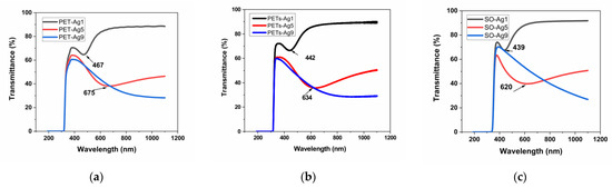
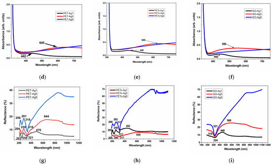
Figure 3.
Optical properties of as-deposited ultrathin films, transmittance, (a) on thick PET, (b) on thin PETs, (c) on optical glass, absorbance, (d) on thick PET, (e) on thin PETs, (f) on optical glass, and reflectance, (g) on thick PET, (h) on thin PETs, (i) on optical glass.
Table 4.
Position of the SPR-specific maxima obtained from the transmittance, absorbance, and reflectance spectra.
The transmittance of the selected samples is over 80% for the sample of 1 nm Ag film thickness and decreases with the thickness of Ag film to about 40% in the case of 9 nm Ag film thickness. The absorbance edge at 300–310 nm for all materials is due to the absorption of the glass or PET substrate [16]. The transmittance maximum is located at about 350 nm for all substrate materials, similar to other authors’ results [5]. As expected, a transmittance minimum appears at increasing wavelengths with increasing thickness for the first two samples, 1 and 5 nm Ag film deposition thickness, respectively, and it is no longer visible in the case of the sample with 9 nm deposition thickness. This confirms the blue-shifted plasmon absorbance when thickness decreases, as observed by other authors [17], but in our case, the displacement is more pronounced. The nature of these minima shown in Figure 3a–c can be explained by the appearance of localized plasmons with the intensity and frequency related to the size of the islands of the film [5]. This minimum, specific for surface plasmon resonance, SPR [5], is located at 467 nm in the case of thick PET substrate, decreasing with substrate thickness to 442 nm, and it is situated at an even lower wavelength, at 439 nm, in the case of the optical glass substrate. This proves the influence of the substrate on the SPR. In the case of samples of 5 nm film thickness, the minimum is displaced toward higher wavelengths, up to 675 nm for thick PET substrate, showing the same decreasing trend with substrate thickness to 634 nm and shifts to a lower wavelength of 620 nm, in the case of the optical glass substrate. The SPR minimum moves toward higher wavelengths (lower energies), with substrate thickness decreasing and film thickness increasing. Other authors, in their reported works, found the minimum attributed to SPR located at about 550 nm for 2 nm Ag film on glass [5], in between our results for SPR in the case of 1 and 5 nm Ag films, respectively. The width and peak position of the SPR were found to depend on the particle size and environment [5,17], similar to our findings related to film thickness and type of substrate.
Each absorbance spectrum from Figure 3d–f presents a broad peak known as the localized SPR band at the wavelength indicated in Table 4 [18]. The maximum of the band corresponds to the SPR wavelength, λSPR [18]. This absorbance maximum specific for SPR appears for the samples of 1 and 5 nm thickness on all substrates, blue shifted with film thickness decreasing for all three substrates and blue shifted with substrate thickness decreasing for PET substrates. The reason for this maximum is that the electromagnetic field of the light wave excites the surface plasmons, leading to absorption [19]. The absorbance maximum for the sample of 1 nm thickness is practically similar to all three substrates, with a tiny blueshift from 442 to 440 nm when PET thickness decreases. For 5 nm thickness samples, the blueshift with substrate thickness decreasing, in the case of PET substrates, is more important, from 645 to 640 nm, but, more than this, for the SO substrate, the blueshift is significant, down to 550 nm, indicating, in this case, a strong effect of the optical glass substrate. The blueshift of λSPR is then more pronounced when the refractive index n of the substrate decreases, knowing that PET has n = 1.57 [20] and SO (BK7 type) has n = 1.516 (Romanian optical glass catalog). Besides the wavelength shift, it can be observed that the resonance band becomes broader as a substrate with a higher refractive index (PET) is used. Two reasons can be responsible for this broadening. One reason is the increasingly enhanced free-electron damping in the dielectric constant of silver when the wavelength increases [13]. The other is due to the particle shape dispersion [18].
The reflectance spectra for PET substrates show two maxima at around 205 and 260 nm, due to the presence of π-electrons of the aromatic part in the molecular chain of PET [16]. The reflectance peak owing to the SPR [16] is observed only for the samples of 1 and 5 nm film thickness, blue shifted on decreasing thickness. The displacement is dependent on substrate type and thickness. The peak is located at 470 nm for thick PET and shifted to 452 nm in the case of thin PET for the samples with 1 nm Ag film, and redshifted as the thickness of film increases to 5 nm, up to 644 nm for thick PET and 630 nm for thin PET. For the SO substrate, compared to PET substrates, a blueshift of the SPR peak appears less pronounced for 1 nm Ag film, shifted only to 446 nm, and more pronounced for 5 nm Ag film, shifted with over 60 nm until 568 nm. In all cases, a blueshift appears as the film thickness decreases. A reflectance minimum is visible in all cases around 320 nm, a few nm higher for thick PET and SO. A roughness influence is perhaps visible in the widening of these maxima in our case, compared to other authors’ works.
Figure 4 presents the graphic determination of Eg [21] for the chosen samples. The Mott and Davis/Tauc equation was applied to obtain the optical band gap, Eg (Figure 4). The equation [21,22]:
allows to determine the band gap, Eg, where α is the absorption coefficient, h is the Planck constant, ν is the light frequency, and n is ½ for the allowed direct electron transitions and 2 for the allowed indirect electron transitions from the valence to the conduction band [23]. For transparent metallic films or for substrate-transparent metallic films (our case), as well as for semiconductors, n takes the value of ½ [23].
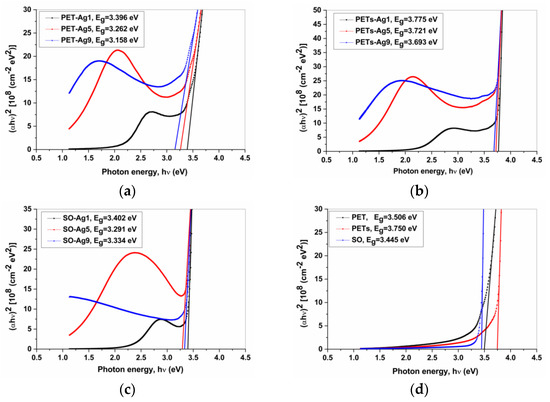
Figure 4.
The bandgap graphical determination for (a) PET-Ag samples; (b) PETs-Ag samples; (c) SO-Ag samples; (d) substrates.
The optical band gap, Eg value, was obtained by extrapolating the linear region of the curve to the zero absorption at which αhν = 0, and the results are presented in Table 5, which summarizes the bandgap (Eg) values for the samples with 1, 5, and 9 nm Ag ultrathin films and the PET, PETs, and SO substrates, and the bandgap displacement (ΔEg) of the substrate-film system from substrate values.
Table 5.
The Eg values for the chosen samples and substrates.
As seen in Figure 4 and from data in Table 5, the bandgap value for the substrate-film system decreases with ultrathin Ag film deposition on every substrate investigated, with one exception, the PETs substrate, but only for 1 nm Ag film. The bandgap value also decreases with the thickness of Ag film increasing for all samples, with an exception, in the case of SO substrate, while for samples with Ag ultrathin film thicknesses of 5 and 9 nm a small increase appears. The most pronounced decrease is visible in the case of PET substrate. These tendencies are normal considering the metallic properties of silver, which decrease the substrate-film system’s bandgap values compared to the substrate bandgap value.
3.4. Ellipsometric Measurements
In the analysis of spectro-ellipsometry data, it is necessary to know the dielectric function of the sample; when this is not known, it becomes necessary to implement a modeling technique.
The dielectric function in the visible region can be calculated from the response of bound and unbound charges to the electric and magnetic fields of light. The Lorentzian equation for the resonant behavior of bound electrons in an electric field is simplified by the Drude model of metals, which is a Lorentzian where the resonance frequency is zero [24].
The Drude–Sommerfeld model assumes that the conduction band electrons react in phase with an applied electric field. In this case, the Drude-Lorentz model becomes [24]:
where ε is the permittivity, ω is the angular frequency, ωp is the Drude plasma frequency defined by [24,25]:
where the electron mass is me and charge, −e, in an external electric field.
The damping constant, Γ, is related to the electron mean free path, l, by [24]:
where υf is the Fermi velocity and τ is the collision frequency. Thus the DC conductivity σ0 of a metal, Ag in our case, may be determined from the Drude model via the relation [24,25]:
The real and imaginary parts of the dielectric constant described by the Drude free-electron theory are [25]:
Here τ(ω) is the relaxation time and ωp is the plasma frequency.
A version of the Drude model [26] with resistivity and mean scattering time as free parameters is described by:
In Equations (8) and (9), adjustable Drude fit parameters are resistivity, ρ (Ω-cm) and scattering time, τ (sec). m* (the carrier effective mass), N (the carrier concentration in cm−3), and μ (the carrier mobility in cm2V−1s−1) are the other parameters. The physical constants are ћ (Plank’s constant/π), ε0 (the vacuum dielectric constant), and the electron charge q (1.6 × 10⁻¹⁹ C).
The ellipsometric ratio ρ = tanψ × exp(iΔ) is determined from the quantities Is and Ic, which are related to the ellipsometric angles ψ and Δ as follows: Is = sin2ψxsinΔ and Ic = sin2ψxcosΔ. The validity of the model is determined by the calculation of a common mean square error function, which accounts for the discrepancies between the measured (IC meas and IS meas) and simulated data (IC calc and IS calc) [27].
Using the Drude model for thin metallic films, the ellipsometric measurements presented as experimental ellipsometric angles ψ (Y in ellipsometer figures) and Δ (D in ellipsometric figures) variation toward the wavelength, experimental and fitted, as shown in Figure 5 for the SO-Ag9 sample, permitted us to calculate [28,29] the variation of the refractive index n with the wavelength, as presented for two of the samples in Figure 6.
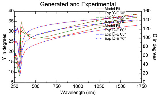
Figure 5.
Ellipsometric angles Y and D, experimental and fitted for the sample SO-Ag9.
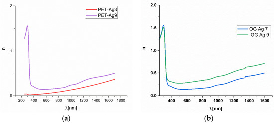
Figure 6.
The variation of refractive index n with the wavelength for Ag deposited on thick PET (a) and optical glass SO (b).
As expected for samples with Ag ultrathin films of several nm, the calculated refractive index in the Vis-NIR domain has values under 0.5 regardless of the substrate of PET or optical glass. Since SPR appeared in ellipsometric measurements, it was difficult to make an accurate fitting of the obtained results in order to obtain the refractive index n and the extinction coefficient k, which was the reason for presenting only the more accurate n values obtained in Figure 6.
The obtained values are close to those indicated by other authors [3,19,25,30]. The tendency observed for our samples is that the refractive index value increases with increasing Ag film thickness for all types of substrates and is not in agreement with data presented in [19], indicating only a small increasing tendency on the Vis-NIR domain. The lowest values for n were observed for the thick PET substrate. The values for the films deposited on a thin PET substrate and SO substrate are close to each other. This proves the influence of the ultrathin films of Ag on the refractive index of the substrate-Ag film system, as the substrate has refractive index values around 1.516 and 1.57 for SO and PET, respectively, resulting in metamaterials systems for the entire domain of Vis and NIR.
4. Conclusions
Ultrathin Ag films of 1 to 9 nm thickness were deposited by RF Magnetron Sputtering onto glass and PET substrates. The samples were morphologically analyzed by atomic force microscopy (AFM), showing roughness of up to 5 nm. SEM investigation confirmed the smoothness and homogeneity of the deposited ultrathin films and showed that the films of 9 nm are continuous. According to the Ag atomic dimension, we concluded that the best possible roughness in conditions of the simple and relatively cheap technique of magnetron sputtering deposition is in the range of 4 atomic layers and 6 atomic layers, which corresponds to λ/50 in the UV domain and λ/100 in the visible domain.
The transmittance and reflectance of the samples, investigated using UV-Vis-NIR spectroscopy, show a transmittance maximum specific to Ag and a minimum transmittance at about 500 nm, which depends on the thickness of the deposited film, clearly showing the surface plasmon resonance at a low thickness of films, meaning up to 9 nm The bandgap value decreases as Ag film thickness increases for all substrate-Ag film systems.
One of the main conclusions of this study is that the films between 5 and 9 nm combine low roughness with potential electrical conductivity because they are continuous films with SPR properties, which make them valuable candidates for future photonic application.
The systems’ refractive index was obtained through spectroscopic ellipsometry data using the Drude model-based technique by minimizing the difference between the measured spectrum of the ellipsometric parameters and the values calculated from the model. The calculated refractive index n presents values of 0.1–0.6 in the 345–1200 nm region.
These results are helpful for using a low-power Magnetron Sputtering technique to deposit ultrathin Ag films as 3D islands or continuous films of low roughness and good surface plasmon resonance, suitable for various applications in photonics.
Author Contributions
Conceptualization, B.A.S. and R.V.M.; methodology, B.A.S., L.B. and R.V.M.; validation, B.A.S. and R.V.M.; formal analysis, R.V.M.; investigation, A.V.F., R.P., N.T., A.A., A.M., M.D., M.C.D., M.O. and M.E.; resources, B.A.S. and R.V.M.; data curation, A.V.F., R.P., N.T., A.A., A.M., M.D., M.E. and M.O.; writing—original draft preparation, B.A.S., A.V.F., M.C.D. and M.O.; writing—review and editing, B.A.S., L.B. and A.V.F.; supervision, B.A.S., A.V.F. and M.E.; project administration, B.A.S.; funding acquisition, B.A.S. All authors have read and agreed to the published version of the manuscript.
Funding
This work was funded by EC in the frame of PULSE-COM, H2020-FETOPEN-2018–2020, 863227 project and by the Romanian Ministry of Research, Innovation and Digitization UEFISCDI, in the frame of the project PN-III-P1-1.1-PD-2021-0682 contract 42/2022, Core Program PN 16N/2019 LAPLAS VI and through Program I—Development of the National R & D System, Subprogram 1.2–Institutional Performance–Projects for Excellence Financing in RDI, contract no. 13PFE/2021. This work was supported by a grant of the Ministry of Research, Innovation and Digitization, CCCDI-UEFISCDI, project number PN-III-P2-2.1-PED-2021-3678, within PNCDI III.
Institutional Review Board Statement
Not applicable.
Informed Consent Statement
Not applicable.
Data Availability Statement
Not applicable.
Conflicts of Interest
The authors declare no conflict of interest.
References
- Jen, Y.-J.; Chen, C.-H.; Yu, C.-W. Deposited Metamaterial Thin Film with Negative Refractive Index and Permeability in the Visible Regime. Opt. Lett. 2011, 36, 1014. [Google Scholar] [CrossRef] [PubMed]
- Prokes, S.M.; Glembocki, O.J.; Cleveland, E.; Caldwell, J.D.; Foos, E.; Niinistö, J.; Ritala, M. Spoof-like Plasmonic Behavior of Plasma Enhanced Atomic Layer Deposition Grown Ag Thin Films. Appl. Phys. Lett. 2012, 100, 053106. [Google Scholar] [CrossRef]
- Gong, J.; Dai, R.; Wang, Z.; Zhang, Z. Thickness Dispersion of Surface Plasmon of Ag Nano-Thin Films: Determination by Ellipsometry Iterated with Transmittance Method. Sci. Rep. 2015, 5, 9279. [Google Scholar] [CrossRef] [PubMed]
- Jalili, S.; Hajakbari, F.; Hojabri, A. Effect of Silver Thickness on Structural, Optical and Morphological Properties of Nanocrystalline Ag/NiO Thin Films. J. Theor. Appl. Phys. 2018, 12, 15–22. [Google Scholar] [CrossRef]
- Axelevitch, A.; Gorenstein, B.; Golan, G. Investigation of Optical Transmission in Thin Metal Films. Phys. Procedia 2012, 32, 1–13. [Google Scholar] [CrossRef]
- Baburin, A.S.; Merzlikin, A.M.; Baryshev, A.V.; Ryzhikov, I.A.; Panfilov, Y.V.; Rodionov, I.A. Silver-Based Plasmonics: Golden Material Platform and Application Challenges [Invited]. Opt. Mater. Express 2019, 9, 611. [Google Scholar] [CrossRef]
- Hajakbari, F.; Ensandoust, M. Study of Thermal Annealing Effect on the Properties of Silver Thin Films Prepared by DC Magnetron Sputtering. Acta Phys. Pol. A 2016, 129, 680–682. [Google Scholar] [CrossRef]
- Marom, S.; Dorresteijn, M.; Modi, R.; Podestà, A.; Di Vece, M. Silver Nanoparticles from a Gas Aggregation Nanoparticle Source for Plasmonic Efficiency Enhancement in A-Si Solar Cells. Mater. Res. Express 2019, 6, 045012. [Google Scholar] [CrossRef]
- Nur-E-Alam, M.; Rahman, M.M.; Basher, M.K.; Vasiliev, M.; Alameh, K. Optical and Chromaticity Properties of Metal-Dielectric Composite-Based Multilayer Thin-Film Structures Prepared by RF Magnetron Sputtering. Coatings 2020, 10, 251. [Google Scholar] [CrossRef]
- Domaradzki, J.; Kaczmarek, D.; Mazur, M.; Wojcieszak, D.; Halarewicz, J.; Glodek, S.; Domanowski, P. Investigations of Optical and Surface Properties of Ag Single Thin Film Coating as Semitransparent Heat Reflective Mirror. Mater. Sci.-Pol. 2016, 34, 747–753. [Google Scholar] [CrossRef][Green Version]
- Zeng, S.; Baillargeat, D.; Ho, H.-P.; Yong, K.-T. Nanomaterials Enhanced Surface Plasmon Resonance for Biological and Chemical Sensing Applications. Chem. Soc. Rev. 2014, 43, 3426. [Google Scholar] [CrossRef] [PubMed]
- Liang, S.; Schwartzkopf, M.; Roth, S.V.; Müller-Buschbaum, P. State of the Art of Ultra-Thin Gold Layers: Formation Fundamentals and Applications. Nanoscale Adv. 2022, 4, 2533–2560. [Google Scholar] [CrossRef] [PubMed]
- Colin, J.; Jamnig, A.; Furgeaud, C.; Michel, A.; Pliatsikas, N.; Sarakinos, K.; Abadias, G. In Situ and Real-Time Nanoscale Monitoring of Ultra-Thin Metal Film Growth Using Optical and Electrical Diagnostic Tools. Nanomaterials 2020, 10, 2225. [Google Scholar] [CrossRef] [PubMed]
- Grachev, S.; de Grazia, M.; Barthel, E.; Søndergård, E.; Lazzari, R. Real-Time Monitoring of Nanoparticle Film Growth at High Deposition Rate with Optical Spectroscopy of Plasmon Resonances. J. Phys. D Appl. Phys. 2013, 46, 375305. [Google Scholar] [CrossRef]
- Zhang, C.; Zhao, D.; Gu, D.; Kim, H.; Ling, T.; Wu, Y.-K.R.; Guo, L.J. An Ultrathin, Smooth, and Low-Loss Al-Doped Ag Film and Its Application as a Transparent Electrode in Organic Photovoltaics. Adv. Mater. 2014, 26, 5696–5701. [Google Scholar] [CrossRef]
- Bumai, Y.A.; Volobuev, V.S.; Valeev, V.F.; Dolgikh, N.I.; Lukashevich, M.G.; Khaibullin, R.I.; Nuzhdin, V.I.; Odzhaev, V.B. Optical Characteristics of Composites Obtained by Ion Implantation of Silver Ions in Polyethylene Terephthalate. J. Appl. Spectrosc. 2012, 79, 773–779. [Google Scholar] [CrossRef]
- Link, S.; Burda, C.; Wang, Z.L.; El-Sayed, M.A. Electron Dynamics in Gold and Gold–Silver Alloy Nanoparticles: The Influence of a Nonequilibrium Electron Distribution and the Size Dependence of the Electron–Phonon Relaxation. J. Chem. Phys. 1999, 111, 1255–1264. [Google Scholar] [CrossRef]
- Xu, G.; Tazawa, M.; Jin, P.; Nakao, S. Surface Plasmon Resonance of Sputtered Ag Films: Substrate and Mass Thickness Dependence. Appl. Phys. A 2005, 80, 1535–1540. [Google Scholar] [CrossRef]
- Charton, C.; Fahland, M. Optical Properties of Thin Ag Films Deposited by Magnetron Sputtering. Surface Coat. Technol. 2003, 174–175, 181–186. [Google Scholar] [CrossRef]
- Nakamura, H.; Shirakawa, Y.; Kitamura, H.; Yamada, T.; Shidara, Z.; Yokozuka, T.; Nguyen, P.; Takahashi, T.; Takahashi, S. Blended Polyethylene Terephthalate and Polyethylene Naphthalate Polymers for Scintillation Base Substrates. Radiat. Meas. 2013, 59, 172–175. [Google Scholar] [CrossRef]
- Elisa, M.; Stefan, R.C.; Vasiliu, I.C.; Iordache, S.M.; Iordache, A.-M.; Sava, B.A.; Boroica, L.; Dinca, M.C.; Filip, A.V.; Galca, A.C.; et al. A New Zinc Phosphate-Tellurite Glass for Magneto-Optical Applications. Nanomaterials 2020, 10, 1875. [Google Scholar] [CrossRef] [PubMed]
- Filip, A.; Musat, V.; Tigau, N.; Polosan, S.; Pimentel, A.; Ferreira, S.; Gomes, D.; Calmeiro, T.; Martins, R.; Fortunato, E. ZnO Nanostructures Grown on ITO Coated Glass Substrate by Hybrid Microwave-Assisted Hydrothermal Method. Optik 2020, 208, 164372. [Google Scholar] [CrossRef]
- Shimakawa, K.; Singh, J.; O’Leary, S.K. Optical Properties of Disordered Condensed Matter. In Optical Properties of Materials and Their Applications; Singh, J., Ed.; Wiley: Hoboken, NJ, USA, 2019; pp. 67–81. ISBN 978-1-119-50631-7. [Google Scholar]
- Oates, T.W.H.; Wormeester, H.; Arwin, H. Characterization of Plasmonic Effects in Thin Films and Metamaterials Using Spectroscopic Ellipsometry. Prog. Surface Sci. 2011, 86, 328–376. [Google Scholar] [CrossRef]
- Jiang, Y.; Pillai, S.; Green, M.A. Re-Evaluation of Literature Values of Silver Optical Constants. Opt. Express 2015, 23, 2133. [Google Scholar] [CrossRef] [PubMed]
- Tiwald, T.E.; Thompson, D.W.; Woollam, J.A.; Paulson, W.; Hance, R. Application of IR Variable Angle Spectroscopic Ellipsometry to the Determination of Free Carrier Concentration Depth Profiles. Thin Solid Films 1998, 313–314, 661–666. [Google Scholar] [CrossRef]
- Todorov, R.; Lozanova, V.; Knotek, P.; Černošková, E.; Vlček, M. Microstructure and Ellipsometric Modelling of the Optical Properties of Very Thin Silver Films for Application in Plasmonics. Thin Solid Films 2017, 628, 22–30. [Google Scholar] [CrossRef]
- Pascu Rovena; Dinescu Maria Spectroscopic Ellipsometry. Rom. Rep. Phys. 2012, 64, 135–142.
- Pascu, V.R. Bilayer Electrolyte Thin Films Gadolinia Doped Ceria /Yttria Stabilized Zirconia Prepared by Pulsed Laser Deposition for Electrochemichal Devices. Rev. Chim. 2020, 70, 4181–4186. [Google Scholar] [CrossRef]
- Palik, E.D. Handbook of Optical Constants of Solids II; Academic Press Inc.: San Diego, CA, USA, 1991; ISBN 978-0-12-544422-4. [Google Scholar]


Publisher’s Note: MDPI stays neutral with regard to jurisdictional claims in published maps and institutional affiliations. |
© 2022 by the authors. Licensee MDPI, Basel, Switzerland. This article is an open access article distributed under the terms and conditions of the Creative Commons Attribution (CC BY) license (https://creativecommons.org/licenses/by/4.0/).