Communication

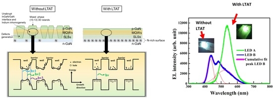
Enhancement in Structural and Electroluminescence Properties of Green Light Emission for Semipolar (11–22) InGaN/GaN Based Grown on m-Plane Sapphire via Low Temperature Ammonia Treatment (LTAT)

1
Low Dimensional Materials Research Centre, Department of Physics, Faculty of Science, Universiti Malaya, Kuala Lumpur 50603, Malaysia
2
Department of Mechanical Engineering, Faculty of Engineering, University of Malaya, Kuala Lumpur 50603, Malaysia
*
Author to whom correspondence should be addressed.
Photonics 2022, 9(9), 646; https://doi.org/10.3390/photonics9090646
Submission received: 22 August 2022 / Revised: 5 September 2022 / Accepted: 6 September 2022 / Published: 8 September 2022
(This article belongs to the Special Issue Advances of Laser Diode and LED)

Abstract

:
Research on enhancement green light emitter is important to obtain a perfect red-green-blue (RGB) induced white light source. Unfortunately the present of mixed phase in deposition of InGaN/GaN limited the potential LED efficiency. Therefore, we introduce a new method called as Low Temperature Ammonia Treatment (LTAT) to eliminate the mixed phase and to enhance the structure properties of InGaN/GaN. Two samples have been prepared, with LTAT (LED A) and without LTAT (LED B). Both samples have been characterized using optical microscope (OM), Atomic Force Microscope (AFM), X-ray rocking curve (XRC) and Electroluminescence (EL). On the structural characterization, the OM results show the present 3D island on LED B sample while sample LED A only shows 2D surface. The RMS surface roughness from AFM are 10.3 ± 0.4 nm and 13.5 ± 10.7 nm for LED A and LED B respectively. XRC analysis proved the LED A with LTAT has a homogenous XRD curve while LED B without LTAT has a mixed phase. The BSFs streak length measured as 1.42 nm−1 and 1.61 nm−1 for LED A and LED B respectively shows low crystallographic defect in LED A compared to LED B. For the EL characteristic, LED A shows a single sharp peak near 538.2 nm wavelength, while LED B shows a broad multi-peak profile at 435.7 nm, 480.6 nm and 520.5 nm. The single sharp peak shows enhancement in green light emission when LTAT is applied during deposition. Successful enhancement is structural and electroluminescence properties shows the effectiveness of LTAT proposed in this work for perfect RGB.

Graphical Abstract

1. Introduction

Over the decades, green light emitter had been fascinated by the group of researchers to unravel the “green gap” in realizing the perfect red-green-blue (RGB)-induced white light source [1,2,3,4]. InGaN-based light emitting diodes (LEDs) have been the well-qualified candidate for green-yellow spectral range emitter by tailoring the indium content in InGaN [5]. Ideally with more indium content incorporated into the multi-quantum wells (MQWs), further redshift can be observed and therefore enable the blue to green-yellow emission. However, the increasing indium composition in the conventional polar c-InGaN results into deterioration of green LED efficiency due to strain-induced polarization which also known as Quantum-confined Stark Effect (QCSE) [6]. Although the current state-of-the-art for green-yellow light emitter grown on c-plane GaN using different novel methods as reported in [7,8,9], yet in recent years, tremendous works have been focused on semipolar InGaN LED, in particularly along the (11–22) plane owing to the reduced piezoelectric polarization and better indium incorporation which favor the growth of longer wavelength LED [10,11,12,13,14].
It is well known that the performance of the InGaN-based LED has been improvised with insertion of the InGaN/GaN superlattice structures (SLSs) as pre layer before the growth of the active region [15,16,17,18,19,20]. By introducing the SLSs as the pre-layers before the first quantum well (QW) growth, the luminescence and efficiency increases significantly with the evidence that such superlattice structures can somehow attribute in the strain-relaxation of QW [21]. Haller et al. had pointed out that the role of the SLSs is to trap the surface defects and avoid them from further incorporate into the QW [22]. It is also reported that the SLSs worked as the strain-relief layers that further reduce the internal polarization fields in MQW [23]. Study of embedded SLSs between semipolar (11–22) Si-doped GaN and the MQWs had been done and proved with a better light output performance as compared to the one without SLSs [18].
Despite all advantages of SLSs mentioned above, it is found that during the growth of semipolar (11–22) InGaN on n-GaN, grown SLSs tend to form unstable mixed phase (10–13) crystallites. According to Zhao et al. [18], prior to growth SLSs, the high growth temperature (1050 °C) of n type GaN is ramped down to a lower temperature < 800 °C. This makes high kinetic barrier for breaking the N-H bond consequently the N precursor generation by ammonia cracking became less efficient even though a larger flow of ammonia is induced [24]. Therefore, it is urgency to produce N-rich ambient which essential for InGaN growth without the present of impurities phaseiu. In this work, our group had observed that ramping down the temperature followed by a Low Temperature Ammonia Treatment (LTAT) where we only let the ammonia gas flow for several minutes. During this process, there is no growth of layer is deposited. The sample that goes LTAT shows an improved results which this had never been reported by others. Thus, in this manuscript, the effect of low temperature ammonia treatment prior to the growth of semipolar (11–22) InGaN/GaN SLSs on the structural and electroluminescence properties of the LED is discussed comprehensively.

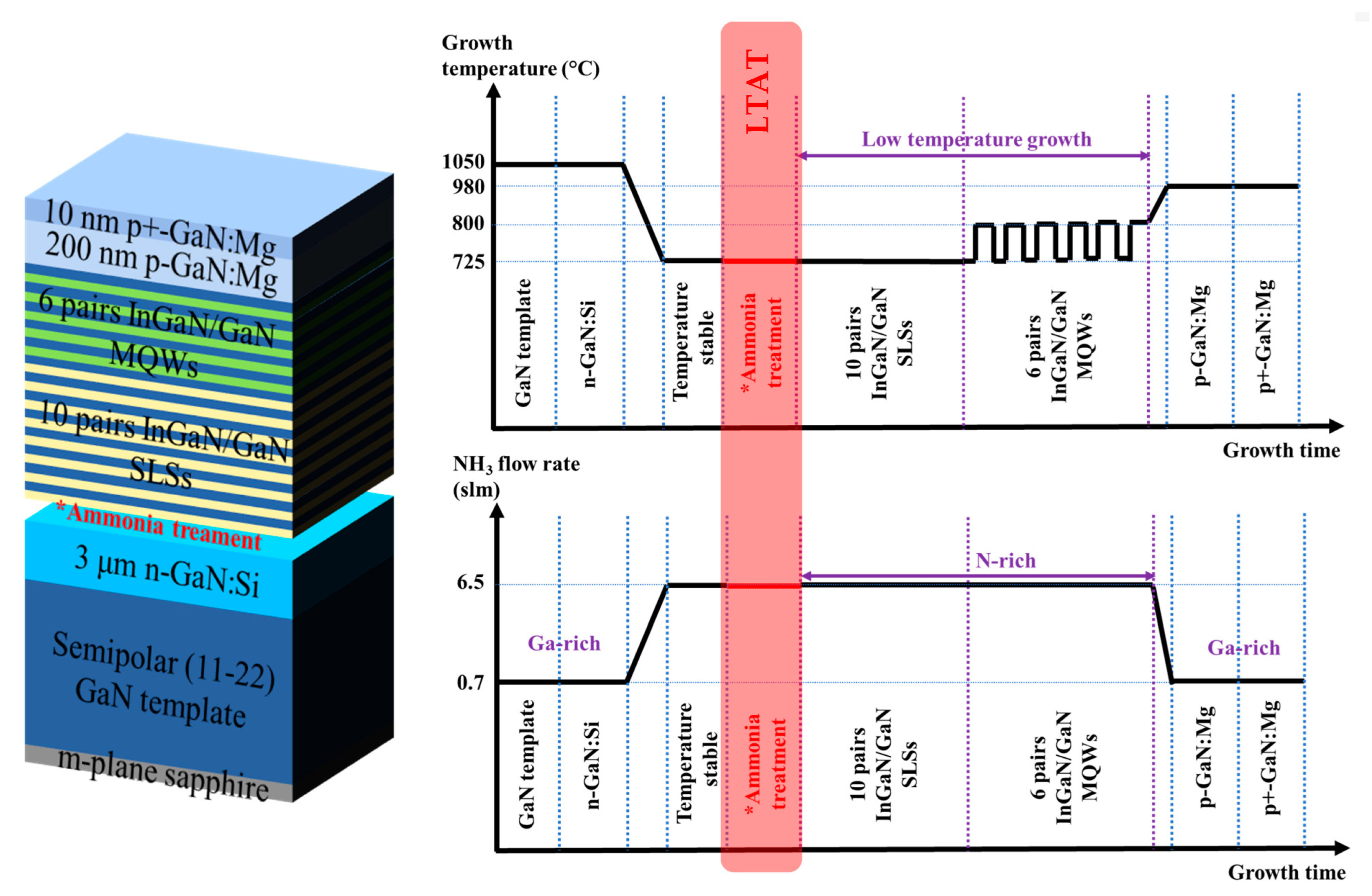
2. Materials and Methods
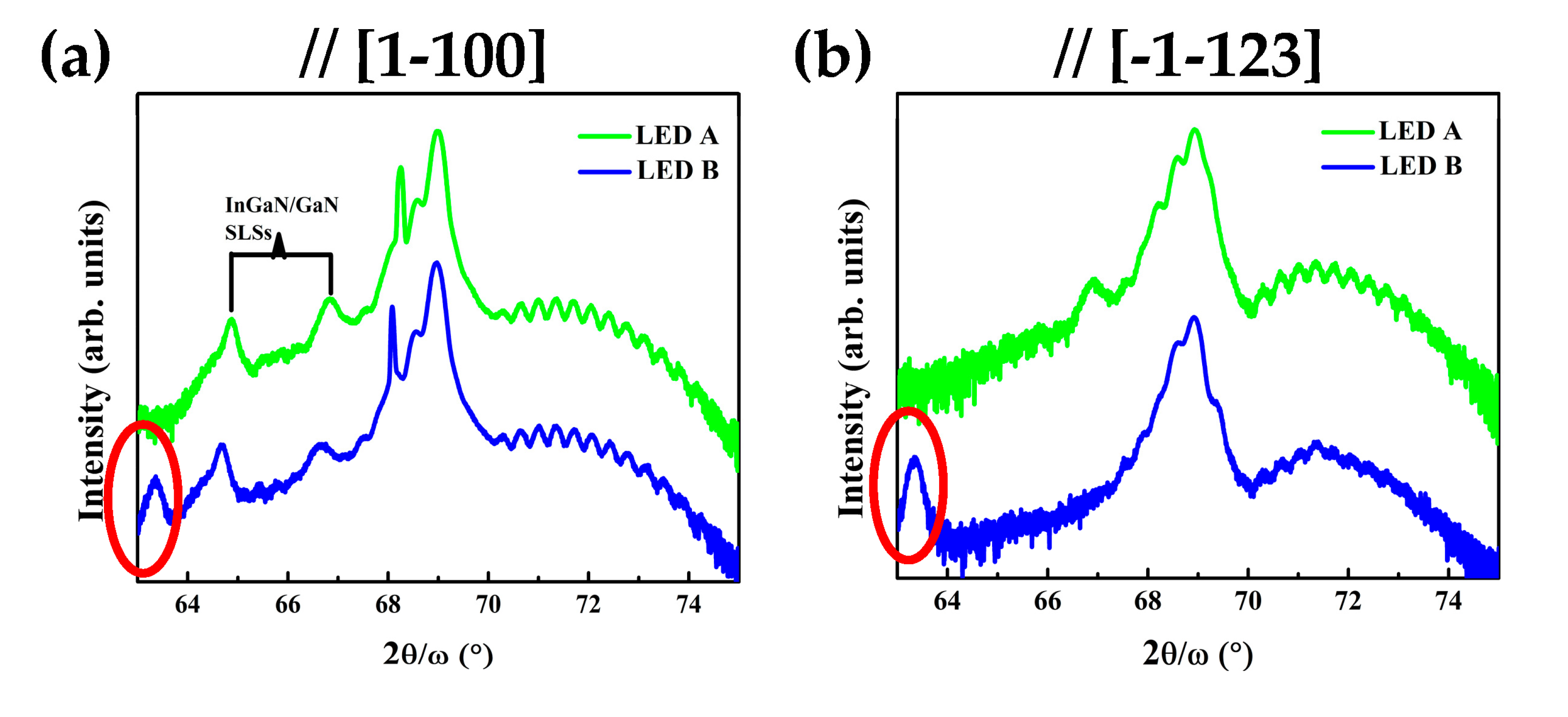
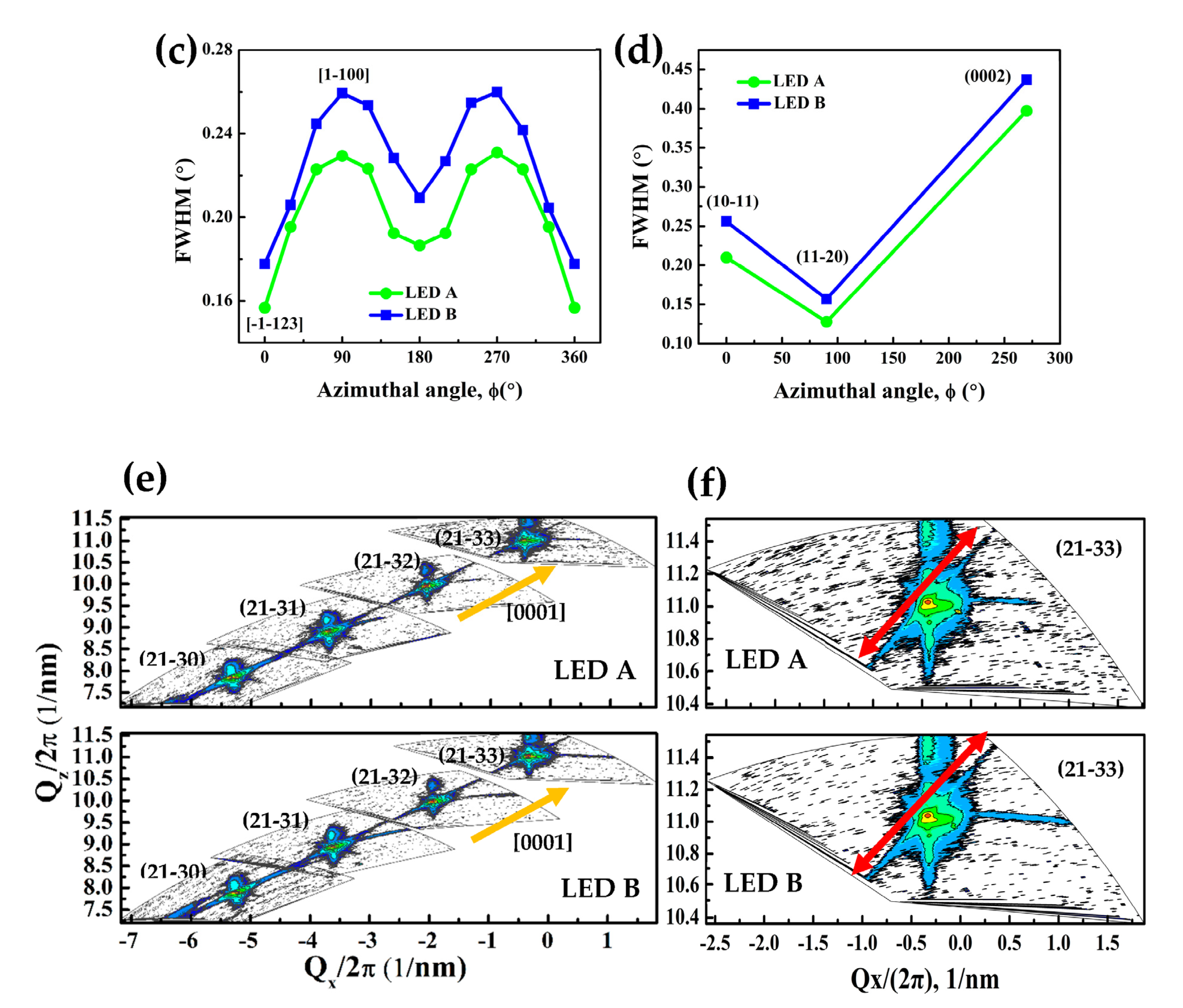
Semipolar (11–22) InGaN/GaN-based LED structure was grown on m-plane sapphire substrate via lateral flow metalorganic vapor deposition (MOCVD) (SR-2000, Taiyo Nippon Sanso Corp., Tokyo, Japan). Trimethylgallium (TMG), triethylgallium (TEG), trimethylaluminium (TMA), trimethylindium (TMI) and ammonia (NH3) were used as the III-V precursor sources, while disilane gas (Si2H6) and bis-cyclopentadienyl magnesium (Cp2Mg) were used as the dopant sources for n-type and p-type GaN respectively. The growth process started with hydrogen cleaning of the substrate inside the reactor at high temperature of 1125 °C followed by the surface nitridation at 1050 °C. The detailed growth to achieve a higher crystal and surface quality semipolar (11–22) GaN template using AlN buffer layer with AlN/GaN multi-layers (MLs) is reported elsewhere [25]. To proceed with the LED structure, 3 µm of Si-doped GaN was grown on the GaN template. At this point, the single crystallinity of (11–22) GaN was confirmed for all the samples and then 10 pairs of 3 nm/3 nm InGaN/GaN SLSs were grown. Prior to the SLS growth, the growth temperature was stepped down to 725 °C and after the temperature was stable, LTAT was carried out by flowing 6.5 slm of NH3 for 14 min without growth any layer. Next, active layers containing 6 pairs of 4 nm/15 nm InGaN/GaN MQWs were grown with TEG: TMI molar ratio of 1:2 succeeded by the growth of 200 nm of Mg-doped and 10 nm of heavily Mg-doped GaN. The reactor pressure was maintained at 13.3 kPa throughout the whole growth process. Here, the LED sample with LTAT was denoted as LED A. For comparison purpose, another LED (LED B) was grown using the identical growth parameters and continuous growth without LTAT. The schematic diagram of the LED structure, growth temperature profile and the ammonia flow profile were illustrated in Figure 1, together with the LTAT step is highlighted in red in the figure. Both LED samples were characterized via Optical Microscopy (OM) (Olympus BX53) and Atomic Force Microscopy (AFM) (TOSCATM 400, Anton Paar GmbH, Graz, Austria) for surface morphology study, High Resolution X-ray Diffraction (HRXRD) (SmartLab, Rigaku Corp., Tokyo, Japan) including 2θ/ω scan, X-ray rocking curve (XRC) on- and off-axis scan, and reciprocal space mapping (RSM) for crystal quality analysis. Prior to the Electroluminescence (EL) analysis, the samples were heated in the furnace at 650 °C for 15 min in air ambient with the purpose of Mg acceptors activation.

3. Results

Figure 2a,b illustrated optical images for samples LED A and LED B respectively. From the images, it is clearly seen 2D surface of sample LED A while the present of 3D islands on the surface of LED B. This 3D island occurred because the lack of N atoms since the cracking efficiency of ammonia dropped rapidly during the transition of growth temperature even though a high flow of ammonia is given. This contributed to the present of mixed phase GaN that favor the growth of 3D island semipolar (11–22) InGaN. It is worth noting in Figure 2b the 3D islands showed an oriental twinning, that the growth directions were 180° with each other results from the present of mixed phase which also reported by Ploch et al. [26]. The present of 3D island in LED B is considered as defect localization spot which will deteriorate the performance of LED B.
Figure 2c,d show the 5 × 5 μm AFM images quantitatively explained the surface morphology of the samples. Characteristic “arrowhead” features were observed for both LED samples where the striations were seldom related to the difference in growth rate for multiple facets in semipolar GaN [27]. For accuracy, measurements were taken on several spots of the sample. The RMS roughness for sample LED A and B was 10.3 ± 0.4 nm and 13.5 ± 10.7 nm respectively. The peak-to-valley value revealed a tremendous difference for sample LED A and LED B, which the values were 76 ± 3.5 nm and 147 ± 146.9 nm respectively. The RMS roughness and peak-to-valley value of LED A showed consistent value while it is observed differently in each spot of LED B due to high 3D island density. The AFM results supported the finding in OM results and also justified the surface enhancement via LTAT in sample LED A. During a low temperature growth of the active region and regardless of the high V/III ambient, the effective V/III is indeed inadequate during the active region growth. With LTAT, the effective V/III can be increased as more N atoms can be dissociated and efficiently enhanced the surface morphology [28].
Figure 3a,b depicted the 2θ/ω scan parallel to [1–100] and [−1–123] direction respectively for sample LED A and LED B. (11–22) GaN peak was recorded at ~69°, while the peak fringes ranged from 70–74° indicated the AlN/GaN multilayers (MLs) from the (11–22) GaN template for both samples. Sapphire (30–30) peak was observed (~68°) along [1–100] scan for both samples, while it is invisible along [−1–123] direction scan due to the tilt between [0001]sapphire and [−1–123]GaN [29]. The lower angle side of GaN peak indicated the InGaN/GaN satellite peaks, where the two peaks at position ~64.5° and ~67° originated from the InGaN/GaN SLSs as observed along [1–100] scan for both samples. Along [−1–123] scan, a peak corresponding to the SLSs (~67°) is observed for LED A while no SLSs peak is detected in LED B. From the simulation results (not shown here), the indium composition in SLS and MQW was ~6% and ~30% respectively for both samples, however the fringes in Figure 3b were obviously observed in sample LED A as compared to LED B which means that the abruptness of the InGaN/GaN layers in LED A were better than LED B. It was well noticed that the existence of peak at ~63.5° in LED B which was corresponding to the mixed phase (10–13) GaN as been noticed in the OM results in Figure 2b [30].
To analyze the crystal quality of the samples, X-ray rocking curve (XRC) ω-scan was performed on (11–22), together with the FWHM results plotted in Figure 3c. From the on-axis scan in Figure 3c, m-shaped plots were observed for both LED samples, yet the FWHM of LED A is lower than LED B with FWHM reduction of ~11% along [−1–123] direction (φ = 0°) and ~12% along [1–100] direction (φ = 90°). The drop in FWHM of (11–22) on-axis scan was primarily due to the reduction in threading dislocations (TDs) density and mosaic tilt in the sample [31]. The off-axis scan in Figure 3d shows the FWHM of (10–11), (11–20) and (0002) for both samples. The off-axis (10–11) and (11–20) rocking curves are broadened by perfect dislocations and prismatic stacking faults (PSFs) respectively, while the broadening of (0002) along c-axis corresponded to partial dislocations (PDs) and/or perfect dislocations [32]. LED A had all the off-axis FWHMs narrowed down by ~20% as compared to LED B, which means LTAT could remarkably improves the crystalline quality of the LED structure [33]. Further analyses are done by calculating basal stacking faults (BSFs) streak that represent order of stacking planes is interrupted in the crystallographic defect. In this analysis, reciprocal space mapping (RSM) was performed at reflection (21–1l) (l = 0, 1, 2 and 3) for sample LED A and B as illustrated in Figure 3e. The orange arrow in the RSM plot (Figure 3e) indicated the direction [0001], where the BSFs streak was aligned [34]. The BSFs streak (21–33) was chosen for further analysis as shown in Figure 3f, the BSFs streak length shown in red arrow is calculated for both samples, that measured as 1.42 nm−1 and 1.61 nm−1 for LED A and LED B respectively. LED A revealed a shorter streak length as compared to LED B which indicated a reduction in BSFs. This further justified the crystalline quality enhancement through LTAT in LED A. From the crystal quality analysis, it is believed that the generation of mixed phase (10–13) crystallite due to limited active nitrogen species induced the 3D islands growth. As the growth mode changing from 2D to 3D, strain was released and more defects and dislocations were generated, which may cause an unabrupt interlayer in the active region [35].
Figure 4 shows the electroluminescence (EL) spectra and the corresponding CIE colour coordinates (CIE 1931 chromaticity diagram) for both LED samples under an injection current of 20 mA. LED A showed a single sharp peak near 538.2 nm wavelength with FWHM of 77.9 nm, while LED B showed a broad multi-peak profile at 435.7 nm, 480.6 nm and 520.5 nm with FWHM 37.3 nm, 43.9 nm and 119.5 nm respectively. The broad multi-peak profile showed that a composition inhomogeneity in the MQW of LED B due to the poor abruptness between the InGaN well and GaN barrier layer. This supported the observation from OM, AFM and XRD results where proved that the low temperature ammonia treatment efficiently improved the abruptness between layers and indium content homogeneity as observed in LED A. From the chromaticity diagram, LED A located at the green region with color coordinate of (0.304, 0.582) while LED B located at a blueish wavelength region at (0.217, 0.255), stated that a better emission at fixed wavelength towards green can be achieved by LTAT prior the active region growth when comparing with standard green in sRGB which has the coordinate of (0.30, 0.60) [36]. As the indium content in realizing green light emission is quite high in this experiment (>25%), it suffers from unstable phases and lead to phase separation and indium inhomogeneity [37]. Through the low temperature ammonia treatment, it effectively suppressed the problems as mentioned above and enhanced a single wavelength green emission.

4. Discussions

In the growth of semipolar (11–22) GaN, ammonia treatment (nitridation) plays a vital role in determining the dominant growth phase of the crystallites, which (11–22), (10–13) and (10–10) are the common orientation grown on m-plane sapphire substrate depending on the ammonia treatment process [26,38]. For the growth temperature of high indium-content InGaN, which ranges 650–850 °C, the cracking efficiency reduces tremendously which suppress the breaking of N-H bonds and causing an inadequate amount of N precursors [24,39]. As the growth temperature decreases during the active region growth whereby a high indium content is required for longer wavelength emission, ammonia treatment became more crucial and here the LTAT is introduced. As discussed in results section, the LTAT reveals an enhancement in structural and electroluminescence properties of green light emission for semipolar (1122) InGaN/GaN based grown on m plane sapphire.
Therefore, it is important to understand the mechanism of LTAT as illustrated in Figure 5. In the deposition without LTAT, as the growth temperature is reduced, the cracking of ammonia becomes less efficient and lead to a reduction in effective V/III on the surface of n-GaN and further produce a mixed phase as been proved from our XRD results, and also demonstrated in others [38,40,41] XRD results present of mixed phase crystallites. While Liu et al. and Foronda et al. [42,43] observed that different V/III will promote different growth preference for (11–22) and (10–13) crystallite. With less N species on the n-GaN surface, (10–13) mixed phase crystallites started to dominate the growth and propagated along the growth direction. This resulted in the 3D islands growth which showed twinning orientation as revealed in the OM results where these had also observed in [26] without further discussion to eliminate the issue. The induced 3D islands were believed to be the defect generation center and caused the unabrupt InGaN/GaN interface with indium inhomogeneity, although some of the defects were terminated with the help of SLS layers. Due to indium inhomogeneity in the quantum wells as illustrated in quantum well band energy diagram without LTAT, it will then produce different localization state with different energy as also describe in [35]. The electron-hole pairs will then recombine with different wavelength emission which as observed in LED B.
In this paper, LTAT is introduced to eliminate the mixed phase and overcome the structure defect. By refer to Figure 5, sample with LTAT, the effective V/III has been improved by flowing ammonia for a period of time as an N-rich ambient is formed during LTAT. Although the cracking efficiency is very low at low temperature, LTAT is believed to help in generate more N-precursors for an N-rich ambient. Since active region is preferably grown on N-rich condition, grow of mixed phase (10–13) crystallites were able to be suppressed and a 2D (11–22) InGaN/GaN growth is promoted. This can be seen in the OM and AFM results which a smoother surface morphology was obtained without any 3D islands. With abrupt interlayers and less defects and dislocation generated, indium can be incorporated into the quantum well evenly throughout the layer as shown in the Figure 5 energy band diagram, the smooth and consistent well to ensure a single wavelength emission as revealed in our EL spectra. All things considered, LTAT plays significant role in achieving a better crystal quality and surface morphology for active region growth, and thus provides a novel enhancement technique for growing semipolar (11–22) green emitter which had not been reported by others.

5. Conclusions

In this study, the growth of semipolar (11–22) InGaN/GaN-based LED structures were performed, and the effect of LTAT on structural and electroluminescence properties were investigated. From the OM and AFM results, sample LED B (without LTAT) possessed a rough surface with emerging mixed phase (10–13) twinning 3D islands, which cause the surface to have high RMS roughness and peak-to-valley value. It is suggested that LTAT in LED A can enhanced the effective V/III and improved the 2D growth of the semipolar (11–22) active region as shown in LED A. Through XRD analysis, the 2θ/ω scan again proved the existence of (10–13) mixed phase crystallites and less obvious fringes were observed in LED B indicated that the unabrupt layers were formed. The X-ray rocking curves suggested an enhancement in crystal quality for LED A in terms of reduction in TDs, mosaic tilt, partial/perfect dislocations and PSFs while RSM proved a reduction in BSF densities via the decrement in BSF streak length along [0001] direction. Via the EL spectra, LED A showed a single peak while LED B revealed a multi-peak profile which justified the indium inhomogeneity due to poor interfaces in the active region. Also, the EL results showed that LTAT enhanced green wavelength emission as a single green wavelength was observed in LED A. With all the results and analysis, a mechanism model is proposed which LTAT improved the effective V/III and suppressed the growth of (10–13) crystallites. Thus, LTAT is believed to enhance structural properties and improve green light emission, although further optimization of parameters for LTAT such as ammonia flow rate and time is needed for a better green emission light.

Author Contributions

Conceptualization, G.T. and A.S.; Methodology, G.T.; Software, G.T. and N.Z.; Validation, A.S., R.N. and Y.H.W.; Formal Analysis, G.T. and N.Z.; Investigation, G.T.; Resources, A.S.; Data Curation, G.T.; Writing—Original Draft Preparation, G.T.; Writing—Review & Editing, R.N.; Visualization, G.T. and Y.J.L.; Supervision, A.S., Y.H.W. and W.H.A.M. All authors have read and agreed to the published version of the manuscript.

Funding

This work is fully financed by Long-Term Research Grant Scheme (LRGS) (LR001A-2016A) granted by Malaysia Ministry of Higher Education (MoHE), Gallium Nitride on Gallium Nitride (GaN-on-GaN) Collaboration Program (PV015-2015) and Targeted Grant (T13C2-17/ PV007-2019) granted by Collaborative Research in Engineering, Science and Technology Center (CREST).

Institutional Review Board Statement

Not applicable.

Informed Consent Statement

Not applicable.

Data Availability Statement

Not applicable.

Acknowledgments

The author would like to thank the members of Nitride Epitaxy and Nanofabrication Laboratory (University of Malaya) for their supports throughout the experiment.

Conflicts of Interest

The authors declare that they have no known competing financial interests or personal relationships that could have appeared to influence the work reported in this paper.

References

  1. Talnishnikh, N.A.; Ivanov, A.E.; Smirnova, A.G.; Shabunina, E.I.; Shmidt, N.M. The contribution of the in distribution in InGaN/GaN MQW to the “green gap” phenomenon. J. Phys. Conf. Ser. 2019, 1199, 012015. [Google Scholar] [CrossRef]
  2. Auf Der Maur, M.; Pecchia, A.; Penazzi, G.; Rodrigues, W.; Di Carlo, A. Unraveling the “Green Gap” problem: The role of random alloy fluctuations in InGaN/GaN light emitting diodes. Phys. Rev. Lett. 2016, 116, 027401. [Google Scholar] [CrossRef] [PubMed]
  3. Massabuau, F.C.-P.; Davies, M.J.; Oehler, F.; Pamenter, S.K.; Thrush, E.J.; Kappers, M.J.; Kovács, A.; Williams, T.; Hopkins, M.A.; Humphreys, C.J.; et al. The impact of trench defects in InGaN/GaN light emitting diodes and implications for the “green gap” problem. Appl. Phys. Lett. 2014, 105, 112110. [Google Scholar] [CrossRef]
  4. Langer, T.; Kruse, A.; Ketzer, F.A.; Schwiegel, A.; Hoffmann, L.; Jönen, H.; Bremers, H.; Rossow, U.; Hangleiter, A. Origin of the “green gap”: Increasing nonradiative recombination in indium-rich GaInN/GaN quantum well structures. Phys. Status Solidi C 2011, 8, 2170–2172. [Google Scholar] [CrossRef]
  5. Usman, M.; Munsif, M.; Mushtaq, U.; Anwar, A.-R.; Muhammad, N. Green gap in GaN-based light-emitting diodes: In perspective. Crit. Rev. Solid State Mater. Sci. 2020, 46, 450–467. [Google Scholar] [CrossRef]
  6. Ding, B. Improving radiative recombination efficiency of green light-emitting diodes. Mater. Sci. Technol. 2018, 34, 1615–1630. [Google Scholar] [CrossRef]
  7. Zhao, X.; Tang, B.; Gong, L.; Bai, J.; Ping, J.; Zhou, S. Rational construction of staggered InGaN quantum wells for efficient yellow light-emitting diodes. Appl. Phys. Lett. 2021, 118, 182102. [Google Scholar] [CrossRef]
  8. Zhao, X.; Tang, B.; Gong, L.; Bai, J.; Ping, J.; Zhou, S. Effect of strain relaxation on performance of InGaN/GaN green LEDs grown on 4-inch sapphire substrate with sputtered AlN nucleation layer. Sci. Rep. 2019, 9, 1–9. [Google Scholar] [CrossRef]
  9. Zhou, S.; Wan, Z.; Lei, Y.; Tang, B.; Tao, G.; Du, P.; Zhao, X. InGaN quantum well with gradually varying indium content for high-efficiency GaN-based green light-emitting diodes. Opt. Lett. 2022, 47, 1291–1294. [Google Scholar] [CrossRef]
  10. Northrup, J.E. GaN and InGaN(112̱2) surfaces: Group-III adlayers and indium incorporation. Appl. Phys. Lett. 2009, 95, 133107. [Google Scholar] [CrossRef] [Green Version]
  11. Monavarian, M.; Metzner, S.; Izyumskaya, N.; Okur, S.; Zhang, F.; Can, N.; Das, S.; Avrutin, V.; Özgür, F.; Bertram, F.; et al. GaN and InGaN (11-22) oriented InGaN-based light emitting diodes. Gallium Nitride Mater. Devices X 2015, 95, 133107. [Google Scholar] [CrossRef]
  12. Zhao, Y.; Yan, Q.; Huang, C.-Y.; Huang, S.-C.; Hsu, P.S.; Tanaka, S.; Pan, C.-C.; Kawaguchi, Y.; Fujito, K.; Van De Walle, C.G.; et al. Indium incorporation and emission properties of nonpolar and semipolar InGaN quantum wells. Appl. Phys. Lett. 2012, 100, 201108. [Google Scholar] [CrossRef]
  13. Wernicke, T.; Schade, L.; Netzel, C.; Rass, J.; Hoffmann, V.; Ploch, S.; Knauer, A.; Weyers, M.; Schwarz, U.; Kneissl, M. Indium incorporation and emission wavelength of polar, nonpolar and semipolar InGaN quantum wells. Semicond. Sci. Technol. 2012, 27. [Google Scholar] [CrossRef]
  14. Choi, J.-H.; Baek, S.-H.; Kim, H.-W.; Na, H.; Lee, S.-N. Indium Localization-Induced Red, Green, and Blue Emissions of Semipolar (11-22) GaN-Based Light-Emitting Diodes. Phys. Status Solidi A 2020, 217, 2000219. [Google Scholar] [CrossRef]
  15. Tsai, C.-L. Effects of underlying InGaN/GaN superlattice structures on the structural and optical properties of InGaN LEDs. J. Lumin- 2016, 174, 36–41. [Google Scholar] [CrossRef]
  16. Ryu, H.-Y.; Choi, W.J. Optimization of InGaN/GaN superlattice structures for high-efficiency vertical blue light-emitting diodes. J. Appl. Phys. 2013, 114, 173101. [Google Scholar] [CrossRef]
  17. Liu, M.; Zhao, J.; Zhou, S.; Gao, Y.; Hu, J.; Liu, X.; Ding, X. An InGaN/GaN Superlattice to Enhance the Performance of Green LEDs: Exploring the Role of V-Pits. Nanomaterials 2018, 8, 450. [Google Scholar] [CrossRef]
  18. Zhao, X.; Huang, K.; Bruckbauer, J.; Shen, S.; Zhu, C.; Fletcher, P.; Feng, P.; Cai, Y.; Bai, J.; Trager-Cowan, C.; et al. Influence of an InGaN superlattice pre-layer on the performance of semi-polar (11–22) green LEDs grown on silicon. Sci. Rep. 2020, 10, 1–8. [Google Scholar] [CrossRef]
  19. Zhou, S.; Liu, X.; Yan, H.; Gao, Y.; Xu, H.; Zhao, J.; Quan, Z.; Gui, C.; Liu, S. The effect of nanometre-scale V-pits on electronic and optical properties and efficiency droop of GaN-based green light-emitting diodes. Sci. Rep. 2018, 8, 1–12. [Google Scholar] [CrossRef]
  20. Zhao, X.; Wan, Z.; Gong, L.; Tao, G.; Zhou, S. Enhanced Optoelectronic Performance of Yellow Light-Emitting Diodes Grown on InGaN/GaN Pre-Well Structure. Nanomaterials 2021, 11, 3231. [Google Scholar] [CrossRef]
  21. Davies, M.J.; Dawson, P.; Massabuau, F.C.-P.; Le Fol, A.; Oliver, R.A.; Kappers, M.J.; Humphreys, C.J. A study of the inclusion of prelayers in InGaN/GaN single- and multiple-quantum-well structures. Phys. Status Solidi B Basic Res. 2014, 252, 866–872. [Google Scholar] [CrossRef]
  22. Haller, C.; Carlin, J.-F.; Jacopin, G.; Liu, W.; Martin, D.; Butté, R.; Grandjean, N. GaN surface as the source of non-radiative defects in InGaN/GaN quantum wells. Appl. Phys. Lett. 2018, 113, 111106. [Google Scholar] [CrossRef]
  23. Lee, K.; Lee, C.-R.; Lee, J.H.; Chung, T.-H.; Ryu, M.-Y.; Jeong, K.-U.; Leem, J.-Y.; Kim, J.S. Influences of Si-doped graded short-period superlattice on green InGaN/GaN light-emitting diodes. Opt. Express 2016, 24, 7743–7751. [Google Scholar] [CrossRef] [PubMed]
  24. Yang, J.; Zhao, D.G.; Jiang, D.S.; Chen, P.; Zhu, J.J.; Liu, Z.S.; Liu, W.; Li, X.; Liang, F.; Liu, S.T.; et al. Investigation on the corrosive effect of NH3 during InGaN/GaN multi-quantum well growth in light emitting diodes. Sci. Rep. 2017, 7, 44850. [Google Scholar] [CrossRef]
  25. Omar, A.-Z.; Shuhaimi, A.; Makinudin, A.H.A.; Khudus, M.I.A.; Supangat, A. Embedded AlN/GaN multi-layer for enhanced crystal quality and surface morphology of semi-polar (11-22) GaN on m-plane sapphire. Mater. Sci. Semicond. Process. 2018, 86, 1–7. [Google Scholar] [CrossRef]
  26. Ploch, S.; Frentrup, M.; Wernicke, T.; Pristovsek, M.; Weyers, M.; Kneissl, M. Orientation control of GaN {112¯2} and {101¯3¯} grown on (101¯0) sapphire by metal-organic vapor phase epitaxy. J. Cryst. Growth 2010, 312, 2171–2174. [Google Scholar] [CrossRef]
  27. Zhao, G.; Wang, L.; Li, H.; Meng, Y.; Li, F.; Yang, S.; Wang, Z. Structural and optical properties of semi-polar (11-22) InGaN/GaN green light-emitting diode structure. Appl. Phys. Lett. 2018, 112, 52105. [Google Scholar] [CrossRef]
  28. Ooi, C.S.; Shuhaimi, A.; Tan, G.; Al-Zuhairi, O.; Majid, W.H.A. Effect of Flux Rate Variation at Fixed V/III Ratio on Semi-Polar (112¯2) GaN: Crystal Quality and Surface Morphology Study. Crystals 2022, 12, 247. [Google Scholar] [CrossRef]
  29. Sun, Q.; Leung, B.; Yerino, C.D.; Zhang, Y.; Han, J. Improving microstructural quality of semipolar (112̱2) GaN on m-plane sapphire by a two-step growth process. Appl. Phys. Lett. 2009, 95, 231904. [Google Scholar] [CrossRef]
  30. Song, K.-R.; Cho, C.-Y.; Lee, S.-N. Effect of a patterned sapphire substrate on indium localization in semipolar (11-22) GaN-based light-emitting diodes. Thin Solid Films 2020, 707, 138077. [Google Scholar] [CrossRef]
  31. Sun, Q.; Han, J. Heteroepitaxy of Nonpolar and Semipolar GaN. Springer Ser. Mater. Sci. 2012, 156, 1–27. [Google Scholar] [CrossRef]
  32. DaSilva, Y.A.R.; Chauvat, M.P.; Ruterana, P.; Lahourcade, L.; Monroy, E.; Nataf, G. Defect structure in heteroepitaxial semipolar (11\bar {2} 2) (Ga, Al)N. J. Phys. Condens. Matter 2010, 22, 355802. [Google Scholar] [CrossRef] [PubMed]
  33. Zhao, G.; Wang, L.; Yang, S.; Li, H.; Wei, H.; Han, D.; Wang, Z. Anisotropic structural and optical properties of semi-polar (11–22) GaN grown on m-plane sapphire using double AlN buffer layers. Sci. Rep. 2016, 6, 1–10. [Google Scholar] [CrossRef]
  34. Pristovsek, M.; Frentrup, M.; Zhu, T.; Kusch, G.; Humphreys, C.J. X-ray characterisation of the basal stacking fault densities of (1122) GaN. CrystEngComm 2021, 23, 6059–6069. [Google Scholar] [CrossRef]
  35. Meng, Y.; Wang, L.; Zhao, G.; Li, F.; Li, H.; Yang, S.; Wang, Z. Red Emission of InGaN/GaN Multiple-Quantum-Well Light-Emitting Diode Structures with Indium-Rich Clusters. Phys. Status Solidi A 2018, 215, 1800455. [Google Scholar] [CrossRef]
  36. Ware, C. (Ed.) Color. In Information Visualization, 4th ed.; Morgan Kaufmann: Burlington, MA, USA, 2021; pp. 95–141. [Google Scholar] [CrossRef]
  37. Chuo, C.-C.; Chang, M.N.; Pan, F.-M.; Lee, C.-M.; Chyi, J.-I. Effect of composition inhomogeneity on the photoluminescence of InGaN/GaN multiple quantum wells upon thermal annealing. Appl. Phys. Lett. 2002, 80, 1138–1140. [Google Scholar] [CrossRef]
  38. Frentrup, M.; Ploch, S.; Pristovsek, M.; Kneissl, M. Crystal orientation of GaN layers on (101 0) m -plane sapphire. Phys. Status Solidi B Basic Res. 2011, 248, 583–587. [Google Scholar] [CrossRef]
  39. Mesrine, M.; Grandjean, N.; Massies, J. Efficiency of NH3 as nitrogen source for GaN molecular beam epitaxy. Appl. Phys. Lett. 1998, 72, 350–352. [Google Scholar] [CrossRef]
  40. Omar, A.-Z.; Bin Abu Bakar, A.S.; Makinudin, A.H.A.; Khudus, M.I.M.A.; Azman, A.; Kamarundzaman, A.; Supangat, A. Effect of low NH3 flux towards high quality semi-polar (11-22) GaN on m-plane sapphire via MOCVD. Superlattices Microstruct. 2018, 117, 207–214. [Google Scholar] [CrossRef]
  41. Maliakkal, C.B.; Rahman, A.A.; Hatui, N.; Chalke, B.A.; Bapat, R.D.; Bhattacharya, A. Comparison of GaN nanowires grown on c-, r- and m-plane sapphire substrates. J. Cryst. Growth 2016, 439, 47–53. [Google Scholar] [CrossRef]
  42. Liu, Z.; Nitta, S.; Usami, S.; Robin, Y.; Kushimoto, M.; Deki, M.; Honda, Y.; Pristovsek, M.; Amano, H. Effect of gas phase temperature on InGaN grown by metalorganic vapor phase epitaxy. J. Cryst. Growth 2019, 509, 50–53. [Google Scholar] [CrossRef]
  43. Foronda, H.M.; Graupeter, S.; Mehnke, F.; Enslin, J.; Wernicke, T.; Kneissl, M. Reducing the grain density in semipolar (11-22) AlGaN surfaces on m-plane sapphire substrates. Jpn. J. Appl. Phys. 2019, 58, SC1026. [Google Scholar] [CrossRef]
Figure 1. Schematic diagram, growth temperature profile and ammonia flow profile for the semipolar (11–22) InGaN/GaN-based LED structure, and * indicating the LTAT step with ammonia treatment (LED A: with LTAT; LED B: without LTAT).
Photonics 09 00646 g001
Figure 2. Optical microscope (OM) under 100× magnification and 5 × 5 μm AFM images for LED sample (a,c) LED A and (b,d) LED B. The red arrows indicated the mixed phase orientation twinning of (10–13) GaN where the growth directions formed 180°.
Photonics 09 00646 g002
Figure 3. (a,b) 2θ/ω scan for sample LED A and B along [1–100] and [−1–123] direction, with red circle indicating the mixed phase (10–13) GaN; (c) On-axis rocking curve FWHM plotted as the function of azimuthal angle; (d) Off-axis rocking curve FWHM of the (10–11), (11–20) and (0002) plane plotted as the function of azimuthal angle, also the reciprocal space mapping (RSM) of (e) (21–3l) reflection (l = 0, 1, 2 and 3) with orange arrow indicating the [0001] direction (BSF streak direction) and (f) (21–33) reflection with red arrow indicating the BSF streak length.
Photonics 09 00646 g003aPhotonics 09 00646 g003b
Figure 4. (a) EL spectra with the inset images of light emission, (b) corresponding CIE color coordinates based on the CIE 1931 chromaticity diagram, of sample LED A and B measured under direct injection current of 20 mA.
Photonics 09 00646 g004
Figure 5. Illustration of the proposed mechanism for LTAT.
Photonics 09 00646 g005
Publisher’s Note: MDPI stays neutral with regard to jurisdictional claims in published maps and institutional affiliations.

