1. Introduction
Of considerable interest are waveguide structures, the dispersion of which can be controlled by an external potential, which is important for the rapid restructuring of the dispersion curve shape in applied problems of photonics. One possible solution is to use layers of graphene and various planar structures based on it. Due to the unique electronic and optical properties of graphene associated with a gapless linear energy spectrum of charge carriers, structures based on it have a strong plasmon response at terahertz frequencies.
It was shown [
1] that the conductivity of graphene never falls below the minimum value, and the graphene quantum well has very dense quantum energy states and can be used in the manufacture of a photovoltaic cell (for example, in [
2]). The electron transport in graphene was studied in detail in [
3]. In [
4], the frequency dispersion of the dynamic conductivity of a multilayer system of graphene layers and
semiconductors was considered as a function of temperature and carrier concentration; it was shown that a narrow band gap and linearity of the electronic spectrum is a common feature of these materials. A terahertz laser based on an optically pumped graphene bilayer used as an active waveguide structure was proposed in [
5]. In [
6], the possibility of controlling Dirac electrons in graphene using external electric and magnetic fields or by changing the geometry and/or topology of the sample was studied; the effects of electron–electron and electron–phonon interactions in both single-layer and multilayer graphene were also presented. The boundary states at isolated graphene–superconductor transitions were considered in [
7], where it was shown how the formation of these states is stable to the presence of disorder in the form of electron charge inhomogeneities in the graphene layer. In [
8], the terahertz generation based on the stimulated generation of plasmons in a planar array of graphene resonant micro/nanocavities strongly coupled to terahertz radiation was proposed; it was shown that, in this case, the generation regime is provided by a balance between the plasmon amplification and the plasmon damping of radiation. Electromagnetic waves localized near the surface of a semi-infinite dielectric medium coated with a graphene layer in the presence of a strong external magnetic field were studied in [
9], and it was shown that the type of hybrid TE-TM polarized surface plasmons can propagate along the graphene layer. In [
10], localized modes on the surface of a multilayer structure consisting of graphene layers separated by dielectric layers were studied; the existence of deep subwavelength surface modes, which can be associated with electromagnetic Tamm states of negative group velocities (in the THz range), was revealed, and the dispersion properties of these surface modes can be tuned by changing the thickness of the dielectric layer of the coating. In [
11], the incidence of two counterpropagating coherent waves on opposite surfaces of a planar layered–periodic graphene–dielectric structure was studied, and it was shown that, by changing the phase difference of these waves, it is possible to control the intensity of the outgoing waves and the absorption of radiation in the structure.
The formation of plasma waves in a graphene structure makes it possible to concentrate the electromagnetic field near the graphene layers and significantly increase the efficiency of its interaction with the structure. In [
12,
13,
14,
15,
16,
17], the possibility of radiation amplification by graphene with an inverted distribution of charge carriers (electrons and holes) was shown. As a result of the inversion of charge carriers in graphene, when a certain threshold value of optical pumping in the THz range is reached, negative high-frequency conductivity arises, the presence of which can lead to the stimulated generation of THz plasmons in graphene. In [
12], the conductivity of a nonequilibrium two-dimensional electron–hole system in optically pumped graphene was studied, and it was demonstrated that, at sufficiently strong pumping, population inversion can lead to pure negative alternating-current conductivity in the terahertz frequency range, which can be used in graphene-based coherent sources. In [
13], nonequilibrium carriers (electrons and holes) were studied in internal graphene at low temperatures in the far- and mid-infrared range. A terahertz laser based on optically pumped graphene layers and a Fabry–Perot resonator was proposed in [
14]; its pumping scheme corresponds to the optical interband excitation of graphene followed by the emission of a cascade of optical phonons, which provides population inversion for interband transitions in a relatively wide range of THz frequencies. The population inversion and negative dynamic conductivity in internal graphene in the THz frequency range under pulsed photoexcitation at wavelengths of the near/mid infrared range were theoretically studied in [
15]. The amplification of extremely short optical pulses in graphene in the presence of a high-frequency alternating field was also studied in [
16]. Surface plasmons propagating along structures with optically pumped single-layer and multilayer graphene were considered in [
17], and it was shown that, with sufficiently strong optical pumping, the conductivity becomes negative in the THz frequency range due to interband population inversion, which can be used in THz lasers based on graphene.
In a structure consisting of two parallel layers of graphene separated by a thin dielectric barrier layer, the electromagnetic fields of plasmons propagating in these layers interact with each other, which leads to the formation of a single plasmon mode. In [
18], coherent THz sources based on the amplification of a charge density wave (plasmon) in two-dimensional graphene were studied. It was shown that the coupling of plasmons with interband electron–hole transitions in inverted graphene layers can lead to plasmon amplification due to the stimulated emission, while the plasmon amplification values can be very large due to the low group velocity of plasmons and the strong limitation of the plasmon field near the graphene layer. Plasmon modes of spatially separated two-layer graphene were also considered in [
19], where the dispersion of plasmons was obtained in a structure consisting of two parallel graphene monolayers with different carrier densities
and
. Plasmonic TM and TE waveguide modes in a waveguide formed by two parallel graphene layers separated by a dielectric were studied in [
20]. In [
21], analytical calculations were made of the dispersion ratio of surface plasmons for two-layer and monolayer graphene monolayers. It was shown that for parallel pairs of graphene, the dispersion relation of the surface plasmon is divided into two branches, one with a symmetric and the other with an antisymmetric magnetic field. It was theoretically established [
22] that the amplification increment of the THz antisymmetric plasmon mode in two layers of graphene is several times greater than the increment of plasmons in a single-layer structure due to the slowing down of the antisymmetric mode, and the increment of the symmetric mode is approximately two times greater than the increment in one layer of graphene due to the constructive interference of plasmon fields in the layers of graphene. In [
23], the amplification spectrum of THz optical and acoustic plasmon modes in a structure consisting of two identical periodic arrays of graphene microstrips separated by a thin dielectric barrier layer was studied. The dispersion relation for plasma waves in a graphene bilayer was studied in [
24], where the possibility of controlling the energy and group velocity of plasmons by changing the potential difference of the potential difference between graphene layers was shown.
Currently, waveguide structures are relevant, the dispersion of which can be controlled by an external potential, as follows from the above scientific studies. One possible solution is to use graphene layers as control electrodes. The parameters of structures containing graphene can be controlled by changing its chemical potential (Fermi energy ) by an external electric field and creating an inverted state due to optical or injection pumping. In this work, we study the effect of the energy state of the graphene layers on the dispersion properties of a planar waveguide structure consisting of two graphene layers separated by a dielectric barrier layer. The dispersion characteristics for structures with layers of doped and inverted graphene are compared with a change in the chemical potential of the graphene, the permittivity of the intermediate layer, and the distance between the layers. The possibility of amplifying the surface mode in the negative conductivity region of graphene is considered. In this regard, the purpose of this work is to obtain a dispersion relation for symmetric and antisymmetric modes and its numerical analysis. The effect of the chemical potential and barrier layer parameters on the plasmon modes is revealed. The possibilities of controlling the plasmon amplification regimes are analyzed. The paper also reveals additional antisymmetric modes that exist in limited intervals of parameters and are characterized by low phase velocities.
2. Structure and Material Parameters
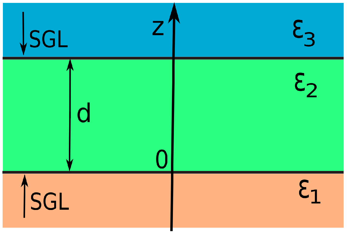
Consider a planar waveguide structure consisting of two layers of activated graphene separated by a dielectric barrier layer of thickness
d and covered with dielectric plates. We will assume that the dielectric permittivity (DP) of the barrier layer
and the plates
,
do not depend on the frequency and are real values (see
Figure 1). The optical response of graphene is largely related to its surface conductivity, which essentially depends on the energy state determined by the chemical potential
. Graphene layers can be in both passive and active states. We will consider graphene passive if the chemical potential is zero, the valence band is completely filled, the conduction band is completely free, and the band gap is absent.
For active graphene, the chemical potential is different from zero, and the nature of filling the energy bands is different. There are doped and inverted graphenes (DG and IG), for which the filling of the conduction and valence bands is different. The frequency dependences of the dynamic surface conductivity of the doped and inverted graphenes within the framework of the Kubo model are determined, respectively, by the expressions [
17,
25,
26,
27]:
where
is the fundamental (static) conductivity of graphene,
e is the charge of an electron,
ħ and
are Planck’s and Boltzmann’s constants,
is the carrier scattering time,
T is the temperature,
is the Fermi energy (for doped graphene) and the quasi-Fermi energy (for inverted graphene). The chemical potential can be controlled by applying a voltage between the graphene sheet and the barrier layer, as a result of which it is possible to change the charge density on the graphene sheet and thereby change the surface conductivity. In unexcited graphene, the chemical potential is at the Dirac point, and applying a voltage of different polarity makes it possible to shift it to the conduction or valence band, doping the graphene with electrons or holes. The charge population inversion in graphene layers can be provided by direct or diffusion pumping of each of the graphene layers [
28,
29]. In this case, the presence of free states in the valence band ensures that the real part of
is negative, as a result of which amplification of propagating waves in the considered structure is possible.
Figure 2 shows the frequency dependence of the real part conductivity of the doped and inverted graphenes
, obtained at
K,
ps (hereinafter) and values of the chemical potential
eV (curves 1–3), the dashed curve corresponds to the value
. It can be seen that the real part of the conductivity for doped graphene takes only positive values in the entire frequency range and for all values of the chemical potential, while negative values are realized for inverted graphene in the frequency range
(5–50) THz. Analysis of expressions (
1) also shows that the imaginary part of the conductivity remains positive over the entire frequency range, has a monotonically decreasing nature of the hyperbolic type, which is similar for both types of graphene and does not have significant features.
3. Fields in the Structure and the Dispersion Relation
Let us write the solution of the Maxwell equations in the form of a surface TM wave (plasmon–polariton), whose electric and magnetic fields decrease with distance from the graphene layers:
where
,
. Stitching the wave fields at the boundaries of the structure, taking into account the electrodynamic boundary conditions
we find expressions for constants
in relations (
2):
is the normalization constant, and the general dispersion relation (DR) for the considered waves localized on the graphene layers in the structure:
This dispersion relation, taking into account the complexity of the parameters included in it, determines the dependence of the real and imaginary parts of the propagation constant on the wave frequency. Note that the form of the DR does not depend on the energy state of the graphene layers, because it is determined by the structure (two layers of graphene) and the type of wave propagating in it. In what follows, we confine ourselves to considering a structure with symmetrical plates, i.e.,
, and, therefore,
, for which the dispersion relation takes the form:
In expressions (
5) and (
6), the conductivity of each of the graphene layers depends on the chemical potential and quasi-Fermi energy (for DG and IG, respectively), which can be controlled during measurements. Below, we consider three important “pair” states of graphene in the structure, which are determined by the value of the chemical potential on each of the graphene layers: symmetric at
, antisymmetric at
, and asymmetric at
,
.
It is also necessary to pay attention that in the symmetric case in Equation (
6), the denominator will contain a full square, which will somewhat simplify the equation and its analysis. In the case, the conductivities will be equal
and the dispersion relation (
6) takes the form of the equation
which breaks down into two separate solutions corresponding to the symmetric and antisymmetric field distributions:
The above equations coincide with the dispersion relations obtained for the case under consideration in [
22]. The modes corresponding to Equation (
8) will be called antisymmetric, and those corresponding to Equation (
9) will be called symmetric, in accordance with the distribution relative to the symmetry plane of the longitudinal (tangential)-field component
.
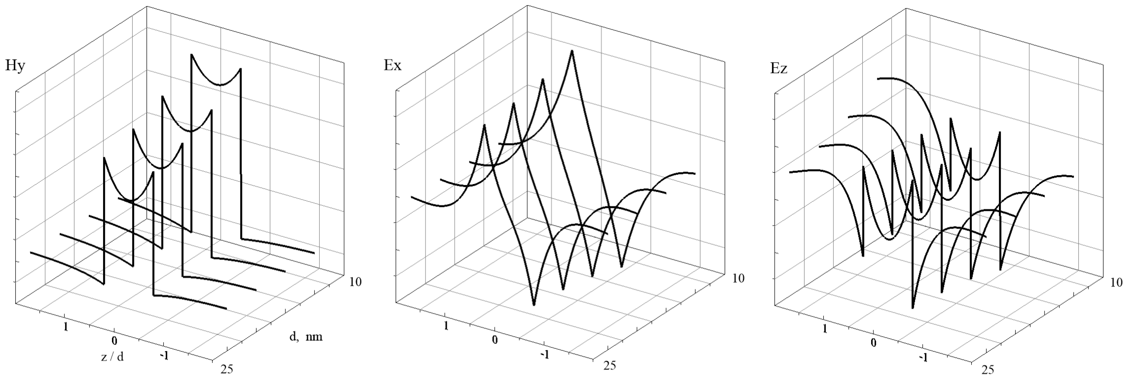
Figure 3 shows the distribution of three components of the
wave field along the
axis, constructed using relations (
2) and (
8) for various values of the barrier layer thickness and
,
eV,
THz. It can be seen that at the layer boundaries (i.e., on graphene sheets), the magnetic field and the normal component of the electric field of the wave suffer a discontinuity and are symmetric, while the tangential component of the electric field is continuous and antisymmetric. With an increase in the thickness of the barrier layer, the amplitudes of all components of the total wave field decrease, which is associated with a decrease in the overlap of the fields localized on each of the graphene sheets.
4. Numerical Simulation Results of the Dispersion Relation
Next, we present the results of a numerical analysis of Equation (
8) for antisymmetric plasma modes obtained at
.
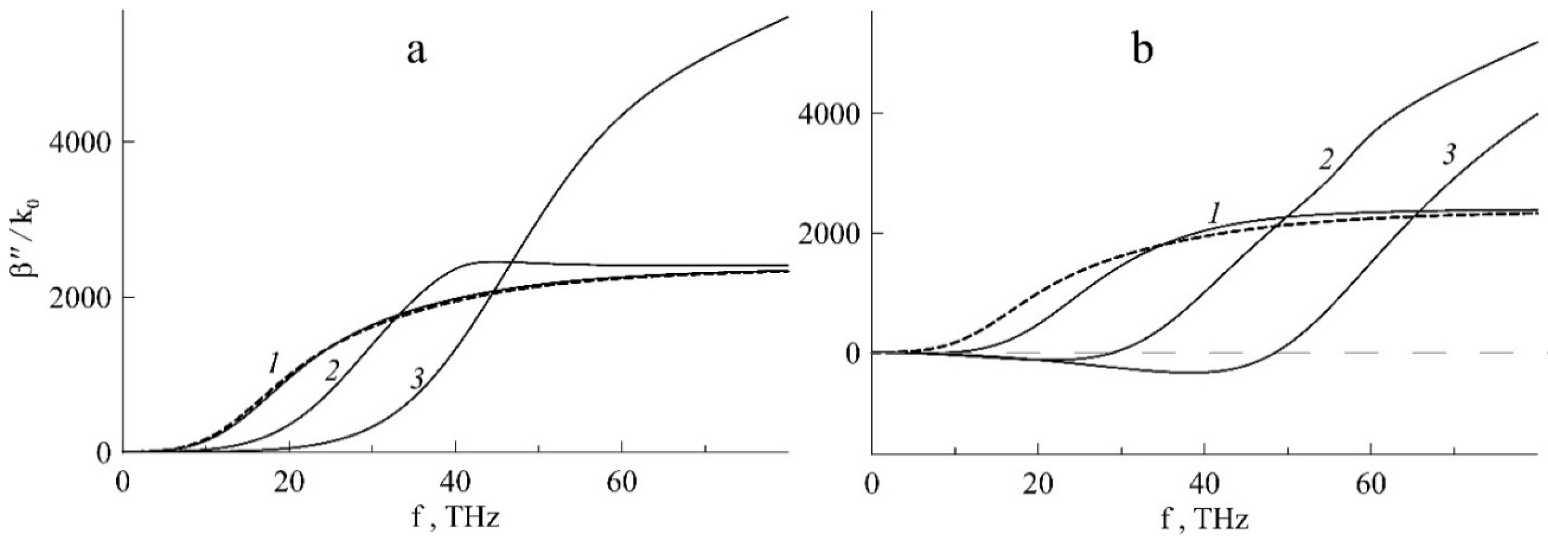
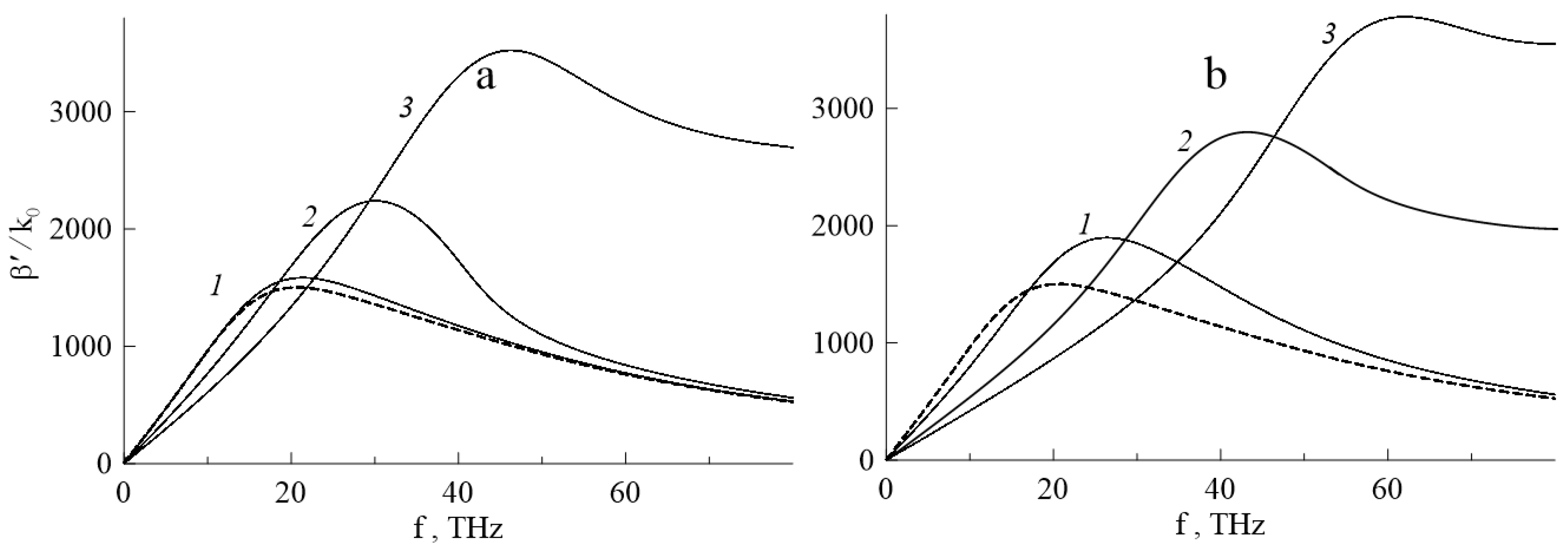
Figure 4, for three values of the chemical potential, shows the frequency dependence of the real part of the propagation constant (normalized to a value
cm
−1 and independent of frequency) of a plasmon-polariton propagating in a structure with DG and IG (a,b). Curves 1–3 correspond to the values
eV. The dashed curve corresponds to the case with zero chemical potential, i.e., the absence of doping and population inversion. In this case, the dependences
for the structures with doped and inverted graphenes are the same. In the initial section up to 20 THz, the value
increases almost linearly with frequency, and the group velocity decreases with increasing
. With a subsequent increase in the frequency, the group velocity decreases and, near the maximum value
, the plasmon–polaritons slow down sharply. The maximum of the curves for the case of the doped graphene always occurs at a lower frequency than in the presence of an inverse-level population. This is due to the position of the minimum of the value
. Although it can be seen that the frequencies for the extrema of the conductivity curves and the propagation constants correlate with each other, they do not coincide anywhere in pairs. Due to the larger value
for the inverted graphene, the contribution to the permittivity turns out to be higher, which causes a shift in the resonant frequency of the curves
. At the frequency where
reaches its maximum, the group velocity vanishes and then changes sign. As the chemical potential increases, the maxima of
shift to the region of higher frequencies and take on ever larger values.
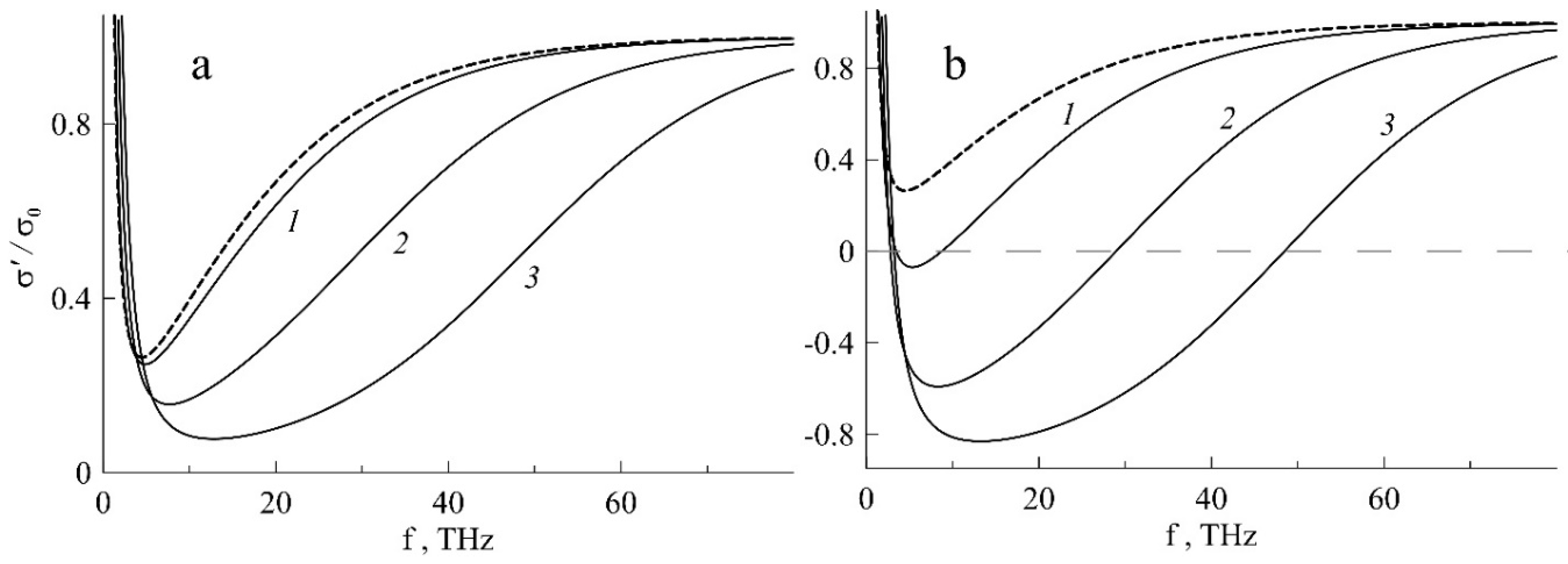
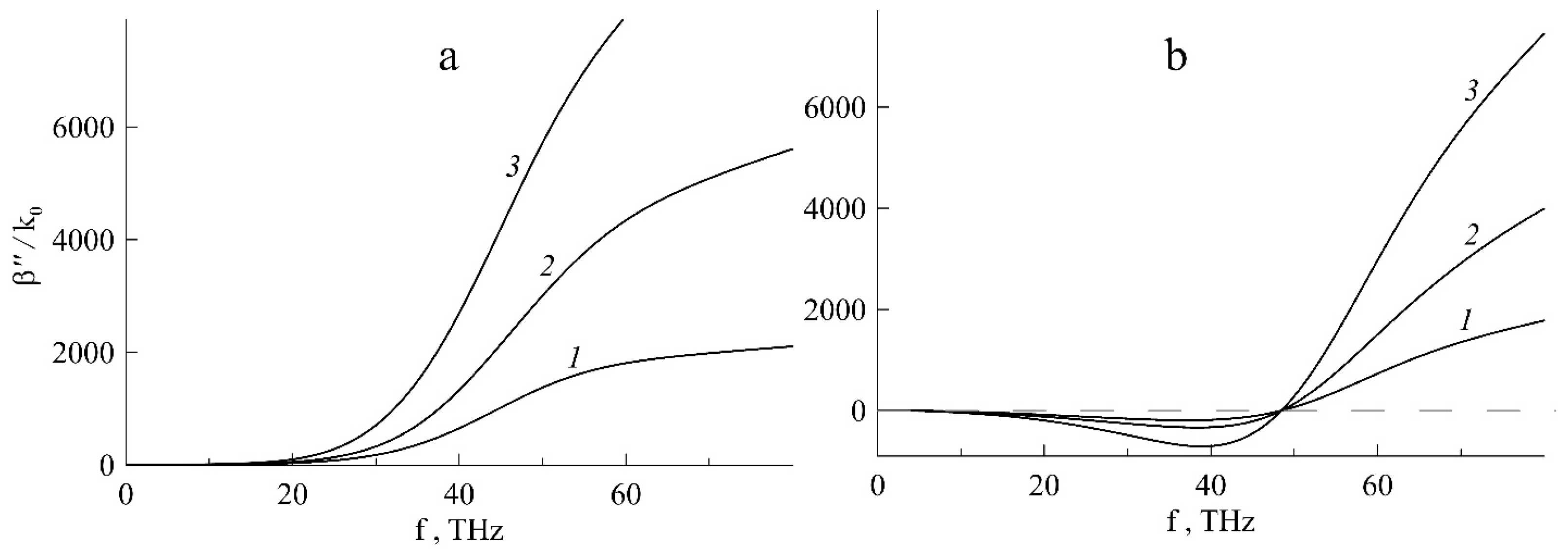
Figure 5 shows the frequency dependence of the imaginary part of the propagation constant for the above values of the chemical potential. For a structure with doped graphene, the value
and therefore the structure is absorbing over the entire frequency range, while for a structure with inverted graphene in the negative region of value
, the value
is also negative, which determines the amplifying properties of the structure in this region. With an increase in the chemical potential in the considered frequency range, a shift toward higher frequencies is observed in the region of a sharp increase in
. In the structure with inverted graphene, the region of negative conductivity expands, which leads to an expansion of the negativity region of the amplification coefficient and an increase in the frequency value corresponding to the minimum (negative) value of
. Waves with a higher frequency are almost completely absorbed in graphene at different path lengths.
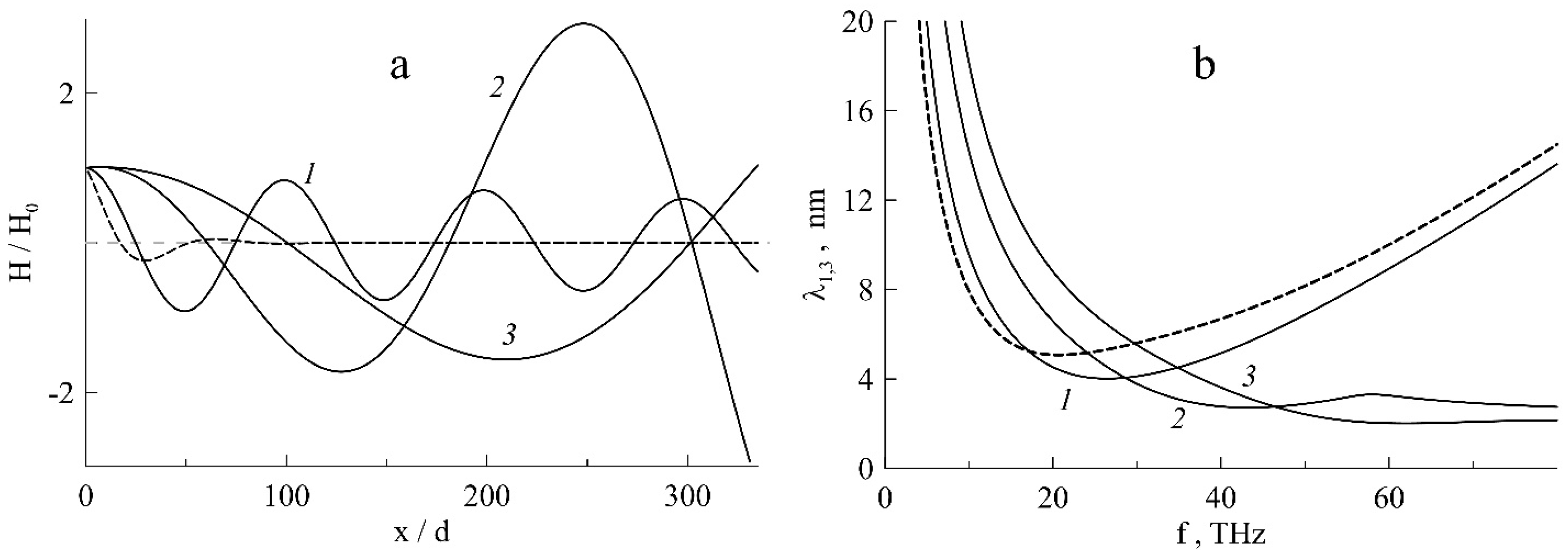
This is confirmed by the coordinate dependence of the wave amplitude along the direction of its propagation, shown in
Figure 6a. In the absence of inversion, the wave damps out as expected. In the case of a small value of the chemical potential (curve 1), the wave damps much more slowly, although the differences for magnitude are about
, and for magnitude, they are about
relative to the case without inversion. In this case, the pump energy is insufficient to maintain even a constant amplitude. Curve 2 corresponds to the almost maximum amplification in the selected frequency interval, so the corresponding wave amplitude noticeably increases. In the case of a larger
, the amplification is also significant, but the frequency at which the maximum amplification is realized is in the region of higher frequencies. Therefore, in the considered frequency interval, the amplitude of such a wave increases but much more slowly (curve 3).
Figure 6b shows the frequency dependence of the depth of the surface plasmon–polariton for a structure with inverted graphene, which shows that, in the considered frequency range, the amplitude of the propagating wave decreases quite rapidly with distance from the boundaries of the structure (graphene layers). The wave turns out to be strongly localized from the outer sides. The field penetration depth into the surrounding space does not exceed a few nanometers, i.e., the field has a sufficiently large amplitude only near the layers.
Figure 7 shows the frequency dependence of the imaginary part of the propagation constant with a different DP of the barrier layer for the structure with DG and IG (a,b),
eV,
nm,
(curves 1–3). It can be seen that with increasing optical density in the structure with doped graphene, the value
(i.e., wave damping) increases monotonically, while in the structure with inverted graphene, the depth of the negative minimum increases, i.e.,
the amplification wave coefficient increases due to the greater polarization of the substance surrounding the graphene layers. In this case, the change in the optical density of the barrier layer has practically no effect on the width of the amplification region. After passing the zero value, the quantity
also increases monotonically with increasing frequency, and the stronger, the larger the value
.
5. Mode Bistability
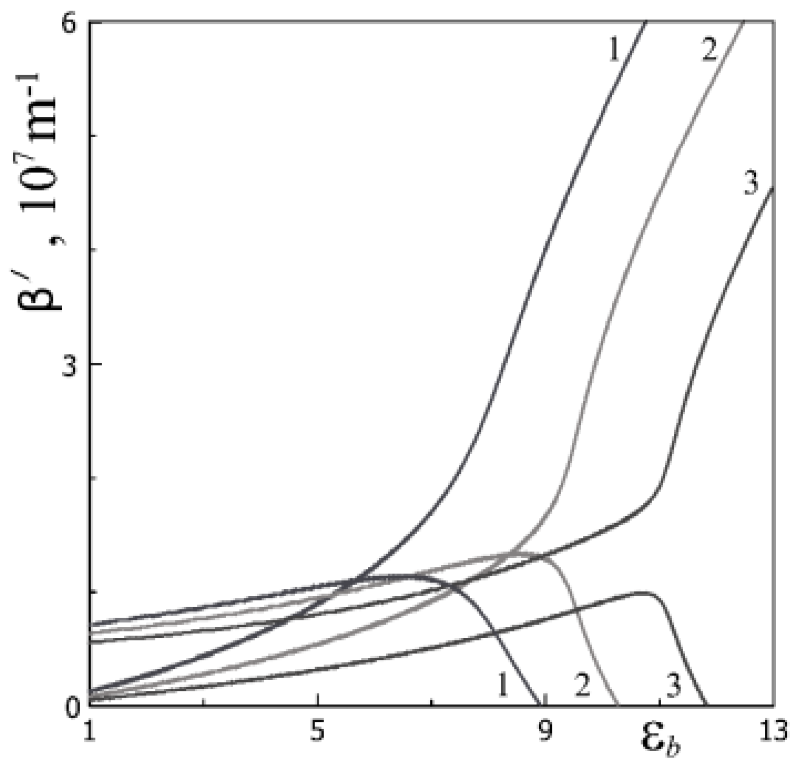
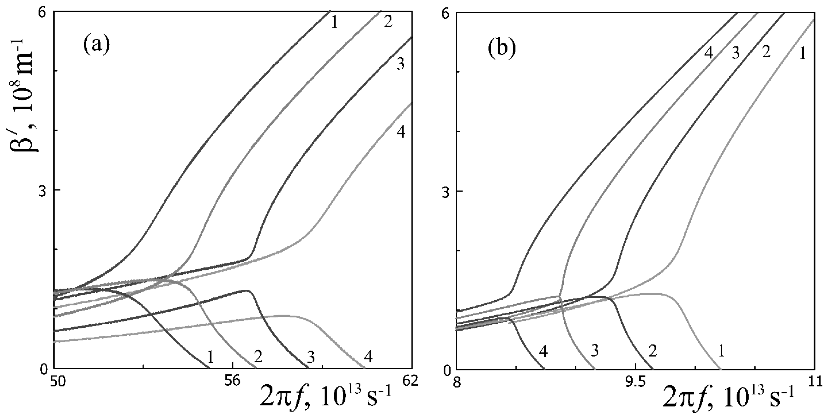
A more detailed analysis of the dispersion relation for the antisymmetric plasmon modes of the considered structure at different values of the parameters showed that additional modes arise in a limited frequency range ( THz), at some frequency interval, and there is a modal bistability. In this case, two modes are realized at one frequency, which differ not only in the magnitude of the propagation constant but also in the sign of the group velocities (in narrower parametric intervals). The phase velocity of these modes decreases strongly in the cutoff region ( Mm−1). In the region of the parameter values close to the mode cutoff, the group velocities of the modes entering the bistability have opposite signs, which can be used to create terahertz radiation generators based on two-layer graphene structures.
Figure 8 shows the dependence of the real part of the propagation constant of the antisymmetric mode on the DP of the barrier layer for a structure with doped graphene for the parameters
nm,
s
−1, and
meV (curves 1–3). From these dependences (similar to the frequency dependences of the propagation constant), it can be seen that additional modes exist in a limited range of parameter values
. Initially, the increase
leads to a slowing increase
of both the main and additional modes (
m
−1), and after passing the maximum of the dependence
(or dependence
), the change rate of the real parts of the plasmon propagation constant increases several times, while the phase velocity of the main modes increases, and the phase velocity of the additional modes drops to small values (near the mode cutoff, in some cases, the numerical analysis gives the value
). With sufficiently thick barrier layers, additional modes do not arise, and only one asymmetric mode takes place in an unlimited frequency range.
The appearance of additional modes is characteristic of a two-layer graphene structure, and these modes were found both in the case of doped and inverted graphene, as well as in the absence of the excitation of the graphene layers. In the case of inverted graphene, additional modes occur in the frequency range where mode amplification takes place. With a significant increase in the thickness of the barrier layer, the graphene layers can be considered isolated, and the additional modes disappear; there are no additional modes in structures with a single graphene layer. These modes are also absent for symmetric plasmons.
Figure 9 shows the cases of modal bistability in the dependences of the real part of the plasmon propagation constant for doped (a) and inverted (b) graphene at various values of the chemical potential and barrier layer thickness. It can be seen from the figure that in the case of doped graphene, the frequency range of the existence of modal bistability increases by a factor of 6, compared with the case of inverted graphene, even at a chemical potential that is two times lower. In the case of the same magnitude
for doped graphene, the purity of the cutoff of the additional mode is an order of magnitude higher than the cutoff frequency of this mode in the case of inverted graphene. Note that not for all the parameters considered in the previous sections, these modes take place. Therefore, in other figures (which, let us emphasize, were not supposed to reflect the full mode composition), additional modes are not shown in order to avoid overloading the graphic information.
6. Discussion
In the experimental papers [
12,
13,
14,
15], it was shown that graphene can be in a passive and active state. Moreover, the active state can be divided into doped and inverted. As a result of numerical simulation, the paper demonstrates the qualitative possibility of controlling the dispersion properties of such a structure by changing the chemical potential of the graphene layers for different parameters of the barrier layer. For the first time, a general dispersion equation is obtained and, for antisymmetric plasmons, a numerical analysis of the dependence of its solutions on the chemical potential, the optical density of the barrier layer, and its thickness is carried out. It is shown that with an increase in the chemical potential value, the region of the amplified waves’ existence in a structure with inverted graphene layers expands. In this case, the maximum value of the amplification coefficient not only increases but also shifts up in frequency.
The dielectric permittivity increase in the layer also contributes to the amplification, because near the graphene layers on the side of the guide layer, the polarization of the dielectric has a significant effect. It is shown that when a certain threshold value of the dielectric layer thickness between the conductive graphene sheets is exceeded, then the graphene sheets cease to interact with each other and cease to affect the shape of the dispersion curve.
For the first time, it is shown that, in a limited frequency range ( THz), antisymmetric plasmons exhibit modal bistability, as an additional antisymmetric mode appears. The phase velocity of this mode strongly decreases in the cutoff region ( Mm−1). In the region close to the mode cutoff, the group velocities of the modes entering the bistability have opposite signs, which can be used to create terahertz radiation generators based on two-layer graphene structures. The existence of the detected additional modes does not critically depend on the specific values of the graphene conductivity and has a clear generality for two-layer graphene structures, because it is observed in the different energy states of the graphene. Questions related to the local modes of a two-layer graphene structure require careful additional research and therefore they are beyond the scope of this article.

