Article

Design and Optimization of a Compact Ultra-Broadband Polarization Beam Splitter for the SCL-Band Based on a Thick Silicon Nitride Platform

by
Georgios Patsamanis
1,2,*,
Dimitra Ketzaki
1,3,
Dimitrios Chatzitheocharis
1,2 and
Konstantinos Vyrsokinos
1,2
1
Centre for Interdisciplinary Research and Innovation, Aristotle University of Thessaloniki, 57001 Thessaloniki, Greece
2
School of Physics, Aristotle University of Thessaloniki, 54124 Thessaloniki, Greece
3
Department of Informatics, Aristotle University of Thessaloniki, 54124 Thessaloniki, Greece
*
Author to whom correspondence should be addressed.
Photonics 2022, 9(8), 552; https://doi.org/10.3390/photonics9080552
Submission received: 6 July 2022 / Revised: 3 August 2022 / Accepted: 4 August 2022 / Published: 6 August 2022
(This article belongs to the Topic Optical and Optoelectronic Materials and Applications)

Abstract

:
The polarization beam splitter is an essential photonic integrated circuit in applications where a high-performing on-chip polarization diversity scheme is required. The lower refractive index contrast of the silicon nitride material platform compared to silicon-on-insulator constitutes the separation of polarized light states a challenging task since for this purpose a large difference between the effective refractive indices of the fundamental TE and TM modes is highly desirable. In this paper, we present the design and optimization analysis of an ultra-broadband polarization beam splitter based on a thick silicon nitride platform through extensive 3D-FDTD simulations. The proposed device exploits two different Si3N4 thicknesses that enable the discrimination of the two polarizations at the proximity of an 800 nm thick slot and a 470 nm thick strip waveguide via directional coupling. The proposed two-stage PBS achieves higher than 30.6 dB polarization extinction ratio (PER) for both TE and TM polarizations across a 130 nm span at the SCL-band. The dimensions of the PBS are 94 × 14 μm2 and the insertion losses are calculated to be lower than 0.8 dB for both polarizations. The fabrication tolerance of the device is also discussed.

1. Introduction

Silicon photonics keeps reporting a remarkable progress on the design and manufacturing of compact and efficient photonic integrated circuits (PICs), paving the way for densely packaged photonic systems combining high-speed operation, low power consumption and cost [1,2]. Both silicon-on-insulator (SOI) and silicon nitride (Si3N4) CMOS-compatible integration platforms address the needs for PICs operating in the near and mid-IR regime for a wide range of applications such as telecommunications, optical signal processing, lidar and sensing [3,4,5]. The functionality of PICs can be significantly enhanced via polarization management and as such Polarization Beam Splitters (PBSs) are vital components towards this direction, as they enable applications requiring polarization-division multiplexing [6,7]. The high refractive index contrast of SOΙ (Δn ≈ 2.0 at 1.55 μm) has led to a maturity and miniaturization of broadband PBS devices with remarkable performance [8,9]. The Si3N4 platform, on the other hand, exhibiting lower index contrast (Δn ≈ 0.52 at 1.55 μm) demands sophisticated approaches in terms of PIC design for the separation of the TE and TM modes. So far, a plethora of Si3N4-based PBSs have been demonstrated relying on different polarization handling mechanisms such as phase-controlled directional couplers (DC) [10,11,12], slot-based DCs [13], multimode interference (MMI) and angled MMI couplers [14,15], cascaded asymmetric DCs [16] and 3D DCs [17]. Although these PBSs take advantage of such well-established polarization splitting techniques, an all-inclusive design for Si3N4 featuring very high performance in terms of minimum polarization extinction ratio (PER) across a large wavelength range (>100 nm), low insertion losses (IL) and small footprint is yet to be reported. The above performance metrics are even harder to achieve in Si3N4 waveguides of more than 600 nm thickness, where the effective refractive indices are almost identical for the TE and TM polarizations. Si3N4 waveguide technology with thickness between 600 nm and 800 nm offers high mode confinement that facilitates frequency comp generation [18], quantum optics [19], optical phased arrays [20], as well as coupling with InP lasers [21], and deploying a high-performing Si3N4 PBS on the same layer thickness would offer remarkable benefits in terms of polarization management.
In this work, we present the design and optimization analysis of an ultra-broadband and compact Si3N4 PBS design that relies on an 800 nm thick slot waveguide and a 470 nm strip waveguide, exploiting the directional coupling scheme and operating in the SCL-band. The structure of the paper is as follows: Section 2 presents the design of a single vertical-slot-based PBS and explains the principle of operation. At this stage, the PBS design is optimized at 1550 nm wavelength, featuring a minimum PER of 13.8 dB across the 1500–1630 nm range for both TE and TM polarizations. Section 3 presents the optimization analysis that is targeting to enhance the minimum PER by maximizing performance at two different wavelengths and applying then a two-stage cascaded formation. The three-dimensional finite-difference time-domain (3D-FDTD) analysis shows then a maximum PER and IL of 30.6 dB and 0.8 dB, respectively, for both TE and TM polarizations with a footprint of only 94 × 14 μm2 across the same SCL-band. Section 4 discusses the tolerance to fabrication errors, when two critical parameters; the thickness of the waveguides and the gap in the DC section deviate independently and simultaneously from their optimized values by Δth = ±16 nm and ΔG = ±20 nm, respectively, resulting to a minimum PER of 22.8 dB in the worst-case scenario that confirms the resilience of the proposed PIC layout. Finally, in Section 5 the proposed PBS design is compared with various state-of-the art Si3N4 counterparts, and the paper concludes summarizing the key results.

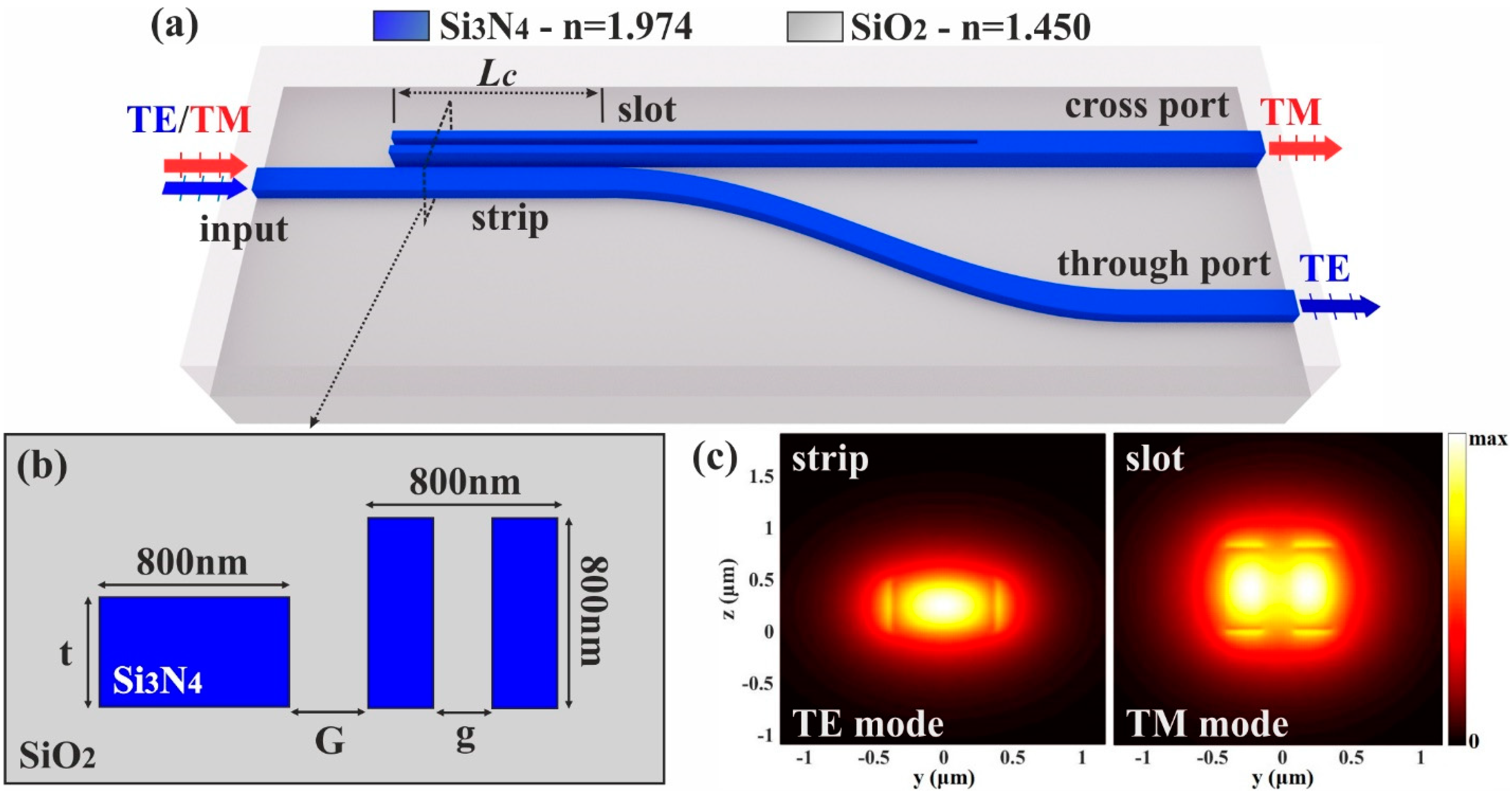
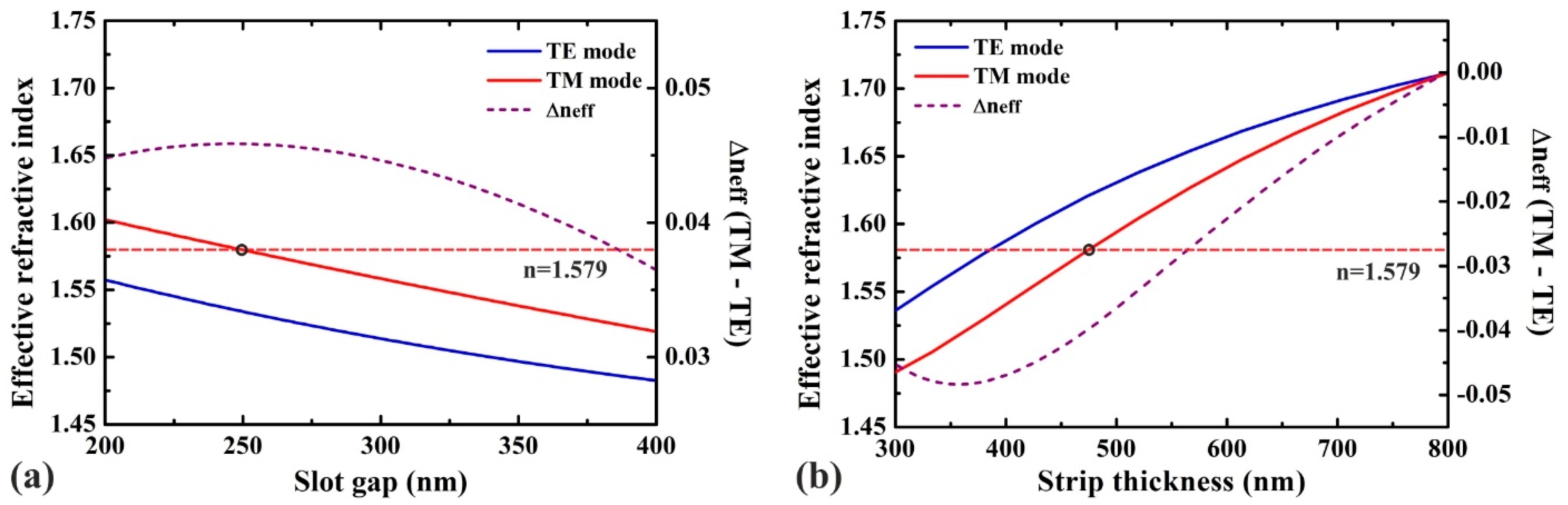
2. Design and Principle of Operation

The proposed all silicon nitride-based PBS consist of an 800 nm thick and 800 nm fixed width vertical slot waveguide with a gap g, and a strip waveguide of thickness t and 800 nm width, as illustrated in the schematic of Figure 1. The TE/TM polarized input light enters the device from the strip waveguide and is split to the two output strip waveguides with different heights. The two types of waveguides support only the fundamental modes, and the polarization selectivity is achieved by ensuring the phase-matching condition for the TM0 mode that is directionally coupled to the slot waveguide and exits the device from the cross port. The TE mode remains at the strip waveguide and exits the device from the through port. The light is exchanged between the two types of waveguides in the coupling section of length Lc, featuring a gap, G. An S-bend is used for the separation of the two ports, with a radius of 50 μm aiming to avoid the induction of any polarization rotation of the fundamental modes, or additional propagation losses. The refractive index n of the Si3N4 waveguides at 1550 nm wavelength is taken as 1.974 and of the surrounding SiO2 cladding as 1.45.
Figure 1b shows the cross-sectional geometry of the two types of waveguides in the coupling region of the DC-based PBS with all fixed values and the parameters under investigation. The supported TE and TM modes of the strip and slot waveguides that eventually propagate to the through and cross ports, respectively, are visualized in Figure 1c. The gap of the slot waveguide is linearly decreased to 150 nm after the coupling region in order to ensure almost lossless transition of the propagating TM mode from the slot to a square 800 × 800 nm2 waveguide, complying simultaneously with the 193 nm DUV lithography limits.

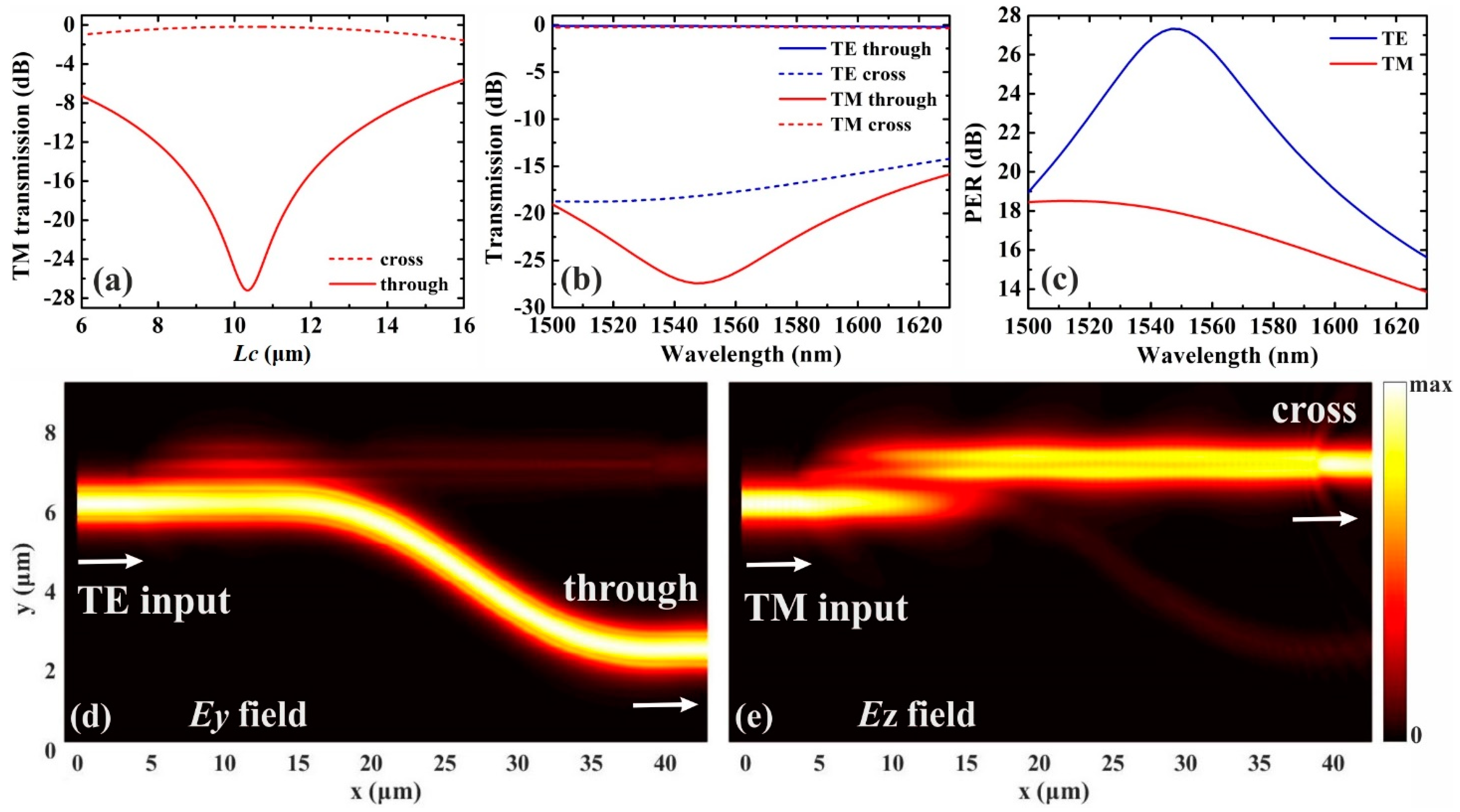
Optimization of the DC-Based PBS for 1550 nm Wavelength

According to the coupled mode theory (CMT) [22], to achieve the phase-matching condition for efficiently coupling evanescently the TM polarized light to the vertical slot waveguide in Figure 1a, the following condition Δ n eff TM = n eff TMstrip n eff TMslot = 0 should be fulfilled by applying the proper combination of design parameters, i.e., g and t, to the two waveguides. On the contrary, the phase-mismatch of the TE polarization can be secured when the highest possible difference between the TE mode effective indices of the strip and slot waveguide, Δ n eff TE = n eff T Ε strip n eff TEslot , is obtained. In this way, the TM polarized light will be coupled with maximum efficiency to the through port, while the TE polarized light will remain uncoupled to the strip waveguide. These conditions are considered quite challenging to meet for the thick (>600 nm) Si3N4 material platform that exhibits (i) a medium refractive index contrast of Δn ≈ 0.5 and ii) close to rectangular waveguide cross sections in contrast to thin (<150 nm) platforms that usually feature an aspect ratio higher than six [23].
The design optimization of the PBS device starts with the calculations of the fundamental TE and TM modes in the slot and strip waveguides for 1550 nm wavelength, by applying the finite-difference eigenmode calculation (FDE) method on the varying cross-sectional geometry. Figure 2a,b shows the calculated effective refractive indices of the TE (blue line) and TM (red line) modes for the slot waveguide with G = 300 nm and varying g, and for the strip waveguide with varying t, along with the respective effective refractive index difference of the modes, Δneff (TM-TE) (purple dashed line), in each case.
According to the results of Figure 2, the mode phase-matching of TM occurs for the combination of g = 250 nm and t = 470 nm, and the effective refractive index of the TM polarization in each waveguide is 1.579, as noted by the horizontal red dotted lines. In addition, the Δ n eff TE value is estimated to 0.086 for these optimum design parameters and can ensure the TE polarized light will propagate to a large degree in the strip waveguide. The Δ n eff ( TM - TE ) curves indicate that the highest Δ n eff TE value of 0.094 is obtained for g = 245 nm and t = 360 nm, but in this case the Δ n eff TM would be only 0.07.
Having specified the proper waveguide geometries, for maximum coupling of the TM mode to the cross port, the design methodology now focuses on calculating the optimum length of the coupling section of the PBS at the coupled waveguide system. The length of parallel waveguides that is required for completely transferring the TM polarization from one waveguide to another is expressed by the beat length Lπ [24]:
L π = λ 2 ( n eff 0 TM n eff 1 TM )
where λ = 1550 nm the central wavelength of operation, and n eff 0 TM and n eff 1 TM the effective indices of the fundamental (even) and first order (odd) TM modes of the coupled waveguide system in the coupling section, respectively. By applying g = 250 nm and t = 470 nm, where Δ n eff TM = 0 and Δ n eff TE = 0.086 as noted, a beating length of Lπ = 15.15 μm is calculated. However, by taking into account the contribution of the S-bend to the light coupling, the actual length Lc will have a lower value than Lπ, that is calculated by a series of 3D-FDTD simulations across the entire structure under investigation. Figure 3a shows the transmission of the TM mode to the cross and through port with varying Lc at 1550 nm wavelength. As expected, the coupling efficiency of the TM mode to the slot waveguide presents a maximum at −0.18 dB around an Lc value of 10.3 μm, while the transmission to the through port has a minimum value of −27.3 dB for this wavelength. The next step is the calculation of the wideband transmission of the TE and TM modes for Lc = 10.3 μm across the 1500–1630 nm wavelength range with corresponding results depicted in Figure 3b. For the TE polarization, the transmission loss to the through port remains above −0.2 dB and to the cross port ranges between −14.2 dB to −18.7 dB. For the TM polarization, the transmission loss to the through port ranges between −15.8 dB and −27.4 dB, while the cross port is above −0.23 dB for the entire span under investigation.
The performance metric of the PBS is evaluated by calculating the polarization extinction ratio (PER) of both polarizations at the corresponding output ports. The PER value is extracted from the equations:
PER TE = T TE through T TM through ,
PER TM = T TE cross T TM cross
where, T TE through , T TM through , T TE cross and T TM cross are the transmitted power of the TE and TM modes expressed in dB at the through and cross ports, respectively, as illustrated in Figure 3b. The PERTE corresponds to the purity of the dominant TE polarization at the through port, while the PERTM to the purity of the dominant TM polarization at the cross port. Figure 3c presents the calculated broadband PER of both polarizations across the investigated 130 nm wavelength span, revealing a minimum value of 15.6 dB for PERTE and 13.8 dB for PERTM. The same figure shows a strong dependency of the PERTE that was expected since the polarization discrimination relies on the wavelength dependent DC mechanism. Regarding the maximum values, the phase-matching and mismatching conditions allow the proposed layout to reach PERTE and PERTM values up to 27.3 dB and 18.5 dB, respectively. In addition, Figure 3d,e illustrate for the proposed optimum conditions the electric field distributions of TE and TM at 1550 nm where the dominant field components are the Ey and Ez, respectively. The IL for this part of the device ranges between 0.04 dB and 0.07 dB for the TE polarization across the whole band and between 0.16 dB and 0.18 dB for the TM polarization, with the extra ~ 0.1 dB mainly associated to the transition via the slot taper. The total length of the PBS design is 36.5 μm, the total width is 6 μm and the gap between the output ports is 4.4 μm.

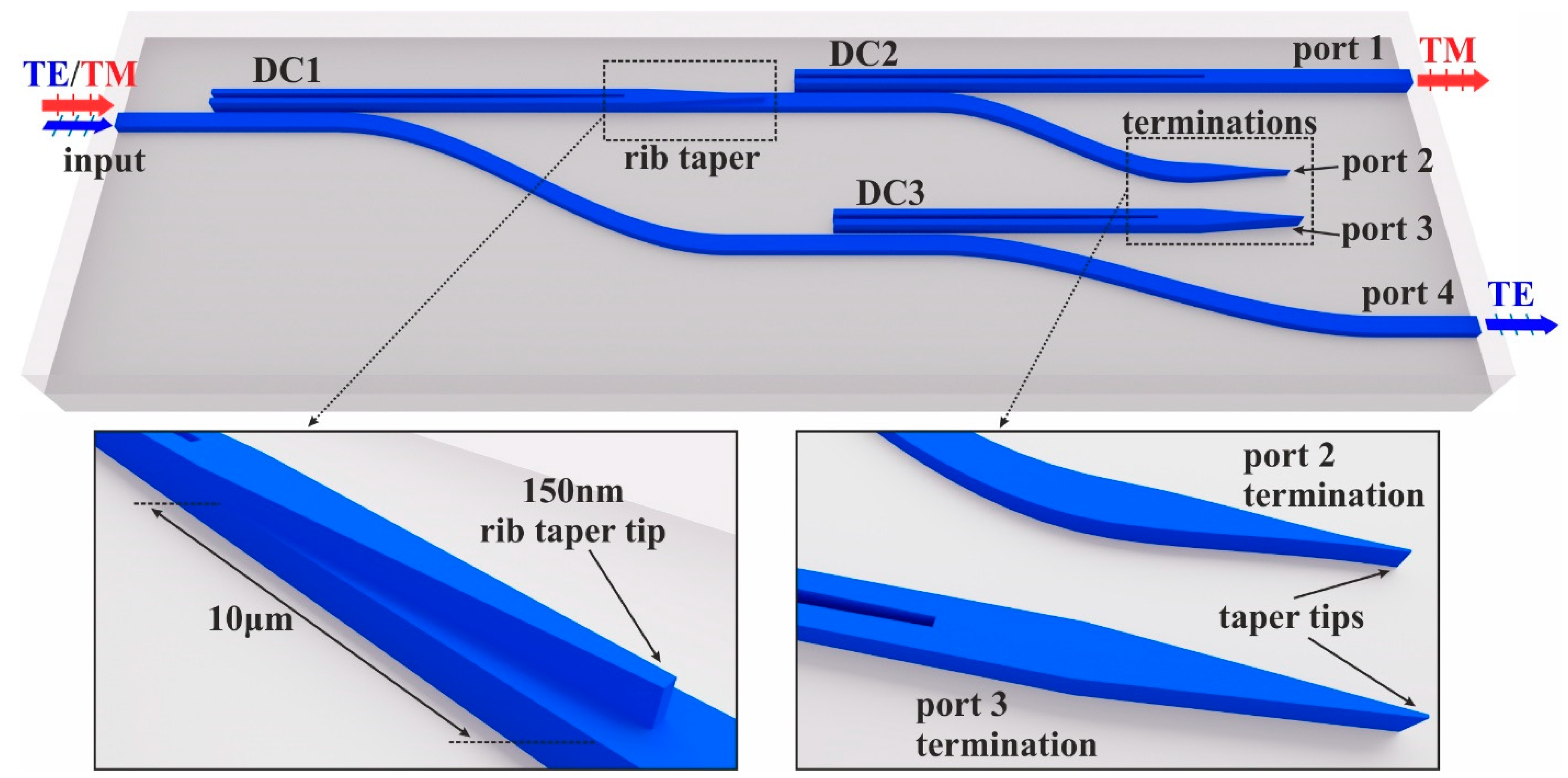
3. Cascaded Formation for Enhanced Performance at Wide Wavelength Range

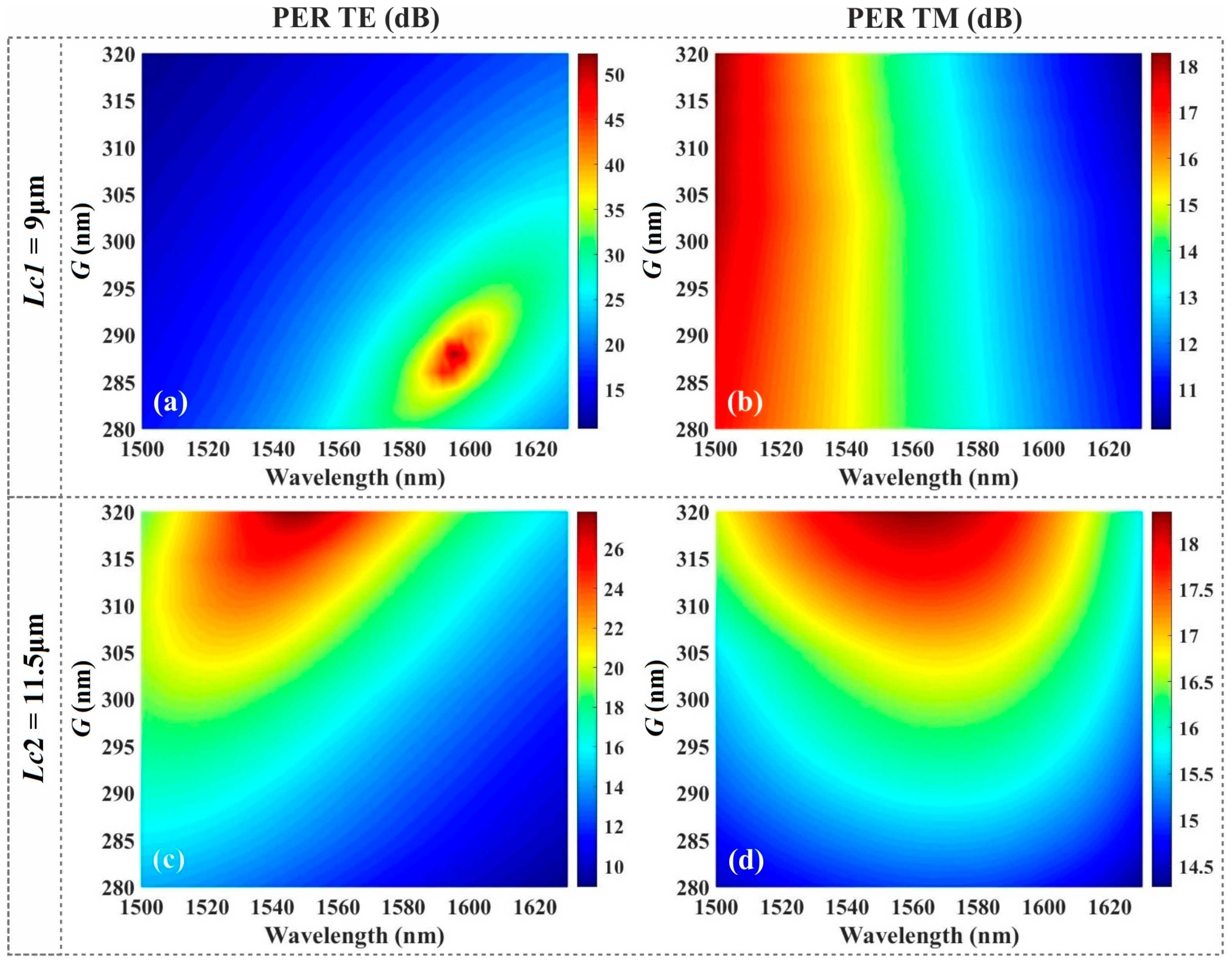
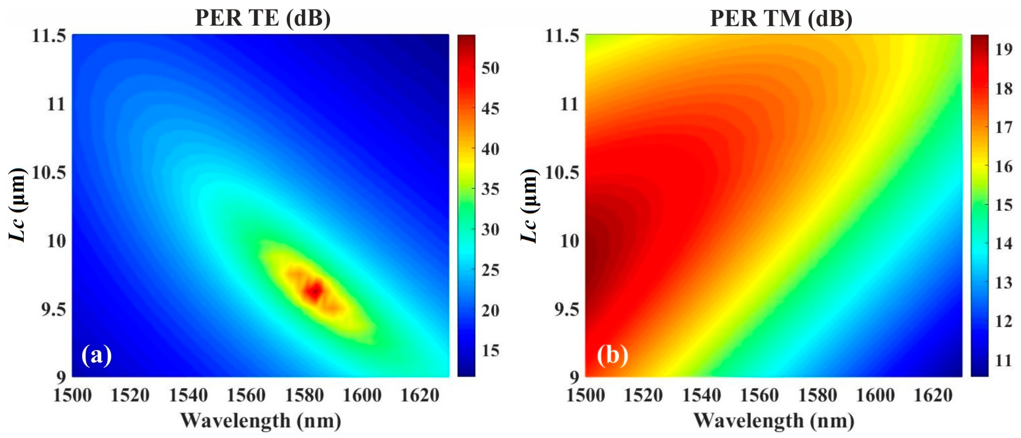
3.1. Variation of Lc and G

The ultra-small size of the proposed PBS grants the oportunity for the investigation of a cascaded layout, aiming towards an ultrahigh broadband performance in terms of PERTE and PERTM, while still maintaining a very low total device footprint. This tailor made performance can be obtained by varying the parameter Lc from 9 to 11.5 μm that adjusts the minimum PERTE and PERTM at the edges of the targeted wavelength span. The combination thus of cascaded PBSs with different Lc provides a device with enhanced performance across the targeted 1500–1630 nm range.
Figure 4 shows the calculated PER over the 1500–1630 nm wavelength range for both polarizations versus the Lc. The TE polarization according to Figure 4a, exhibits PERTE more than 18.8 dB at 1500 nm for Lc > 11 μm, and more than 22.9 dB at 1630 nm for Lc < 9.5 μm. The very high values of PERTE observed around 1580 nm indicate that strong phase-matching in the proposed DC-based PBS also occurs for this wavelength region. The performance for the TM polarization is illustrated in Figure 4b and the PERTM exhibits more than 15.3 dB across the whole wavelength span for Lc = 11.5 μm, while the minimum value is 10.5 dB for Lc = 9 μm at 1630 nm. Overall, the variation of Lc leads to a change in the spectral position of the PERTE peak, while for PERTM the preference is for larger Lc where the minimum value increases. A proper combination thus of these two layouts could deliver the desired broadband performance in terms of PER for both polarizations. The next optimization stage is the investigation of the spectral response for these two Lc, by varying the design parameter G. Figure 5 shows the calculated PERTE and PERTM for Lc1 and Lc2 when G varies between 280 nm–320 nm. According to what is expected, the variation of G leads in a change of the position of the peak of PERTE and of the minimum values of PERTM. Figure 5a reveals that for Lc1 = 9 μm, PERTE is calculated to be everywhere higher than 15 dB with maximum values reached at 1580 nm for G ~ 285 nm. Also, according to Figure 5b, PERTM is higher than 11 dB for G < 285 nm. On the other hand, from Figure 5c for Lc2 = 11.5 μm, PERTE is everywhere higher than 14 dB for G > 315 nm, with maximum values obtained at 1545 nm. Finally, from Figure 5d the minimum PERTM is higher than 15.5 dB for G > 315 nm. Therefore, choosing a PBS with Lc1 and G < 285 nm can increase the minimum values for both PERTE and PERTM and move the peak of PERTE closer to 1580 nm, while choosing Lc2 with G > 315 nm can further boost minimum PERTM and move PERTE closer to 1545 nm. The 3D-FDTD simulations reveal also that the IL remain below 0.23 dB for all Lc and G combinations.

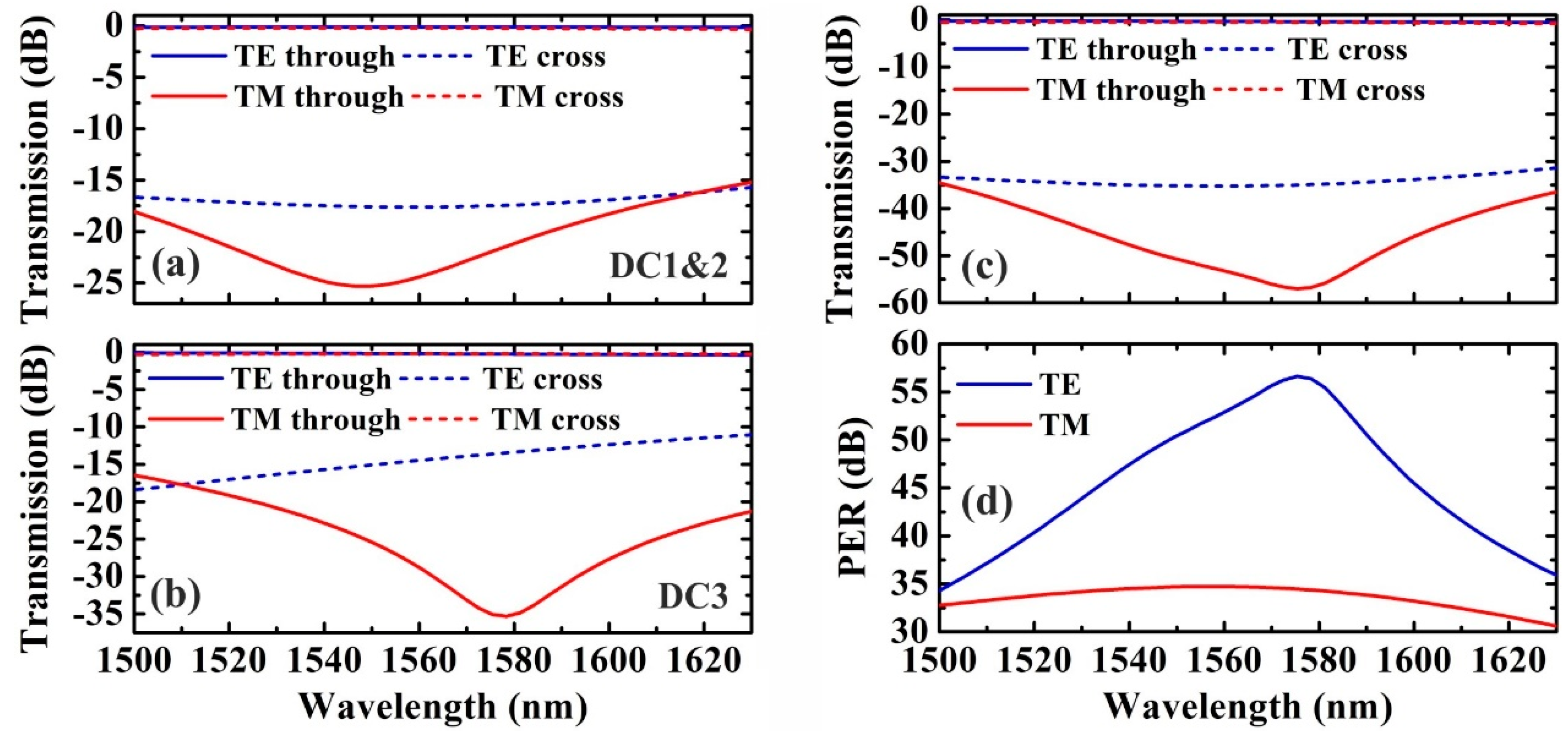
3.2. Cascaded Formation

Having calculated the broadband performance of a single PBS by varying the two major design parameters Lc and G, we proceed to the design and analysis of the two-stage cascaded formation targeting to maximize the PER values across the entire 1500–1630 nm band, at the expense of total dimensions and insertion losses. Figure 6 illustrates the proposed layout where three DCs with different combinations of selected Lc and G are employed. The input light is injected into the PBS from the 470 nm thick strip waveguide to DC1, where the cross/through ports are connected to DC2/DC3, respectively. The transition from DC1 to DC2, as shown in the left inset of Figure 6, is carried out via a 10 μm long rib-type taper with a tip of 150 nm that adiabatically transfers the light from the 800 nm to the 470 nm thick waveguide. The TM polarized light is monitored from the cross port of DC2 referred as port 1, while the TE lightwave is recorded from the through port of DC3, marked as port 4. The through port of DC2 and the cross port of DC3, labeled as port 3 and port 4, respectively, collect the residual unwanted TE and TM light for subsequent suppression of any unwanted back reflections via taper tips. The right inset of Figure 6 shows details about this part of the PBS layout.
The optimum PBS design is coming from a combination featuring identical DC1 and DC2 with Lc2 = 11.5 μm and G = 320 nm, while for DC3 the corresponding key parameters are Lc1 = 9 μm and G = 280 nm. Figure 7a shows the DC1 & DC2 transmission curves for TE/TM polarization and Figure 7b for DC3, both extracted by 3D-FDTD simulations. The two graphs reveal that the IL are below 0.22 dB for DC1 & DC2 and less than 0.23 dB for DC3 with a flat response. Also, from the same graphs it is shown that the minimum PERTE for DC3 is located at 1500 nm with a value of 16.4 dB, while the minimum PERTM is of 10.9 dB at 1630 nm. On the other hand, DC1 & DC2 presents a symmetric performance with a minimum PERTE, PERTM of 15 dB and 15.5 dB respectively, both at 1630 nm. Figure 7c illustrates the calculated aggregated transmission curves of the cascaded DC scheme, extracted from transfer matrix simulations, taking into account the S-parameters of DC1/DC2 and of DC3 from Figure 7a,b. The transfer matrix method was selected at this point, eliminating the need to simulate the entire device with 3D-FDTD that would require enormous computational resources. It should be pointed out that the model also considers in the transfer matrix the IL of the rib taper for the transition between the two different thicknesses that is less than 0.06 dB. This advanced PBS scheme now induces IL in the range of 0.23–0.57 dB for TE light and between 0.48 dB and 0.8 dB for TM polarization in the entire 130 nm window. Figure 7d displays the performance in terms of PER, revealing minimum values of 34.3 dB and 30.6 dB for PERTE and PERTM respectively, granting the ultra-high polarization selectivity in combination with ultra-broadband performance targeted at the start of this work. It should be noted that these high PER values allow high margin for error during fabrication as it will be shown in the next Section.
The total dimensions of the proposed formation are estimated at 94 × 14 μm2 by 2D-layouting and the gap between the output ports 1 and 4 is 12.4 μm. It is worth noting that when deploying the specific DCs of Figure 7, the minimum PER of the device is improved by 3.3 dB and 3 dB for TE and TM polarization, respectively, compared to the layout that employs three identical PBSs of Figure 3c optimized for 1550 nm. In addition, the IL for the TM port can be further reduced by narrowing the tip of the slot tapers down to 50 nm, reaching overall values lower than 0.4 dB. On the other hand, when the width of the slot tip is 250 nm instead of 150 nm, the IL is raised up to 1.4 dB for TM polarization. For the TE light the corresponding values are 0.5 dB for 50 nm and 0.9 dB for 250 nm slot gap. Table 1 summarizes the design parameters of the PBSs in the proposed cascaded scheme and their performance across the 1500–1630 nm wavelength range.

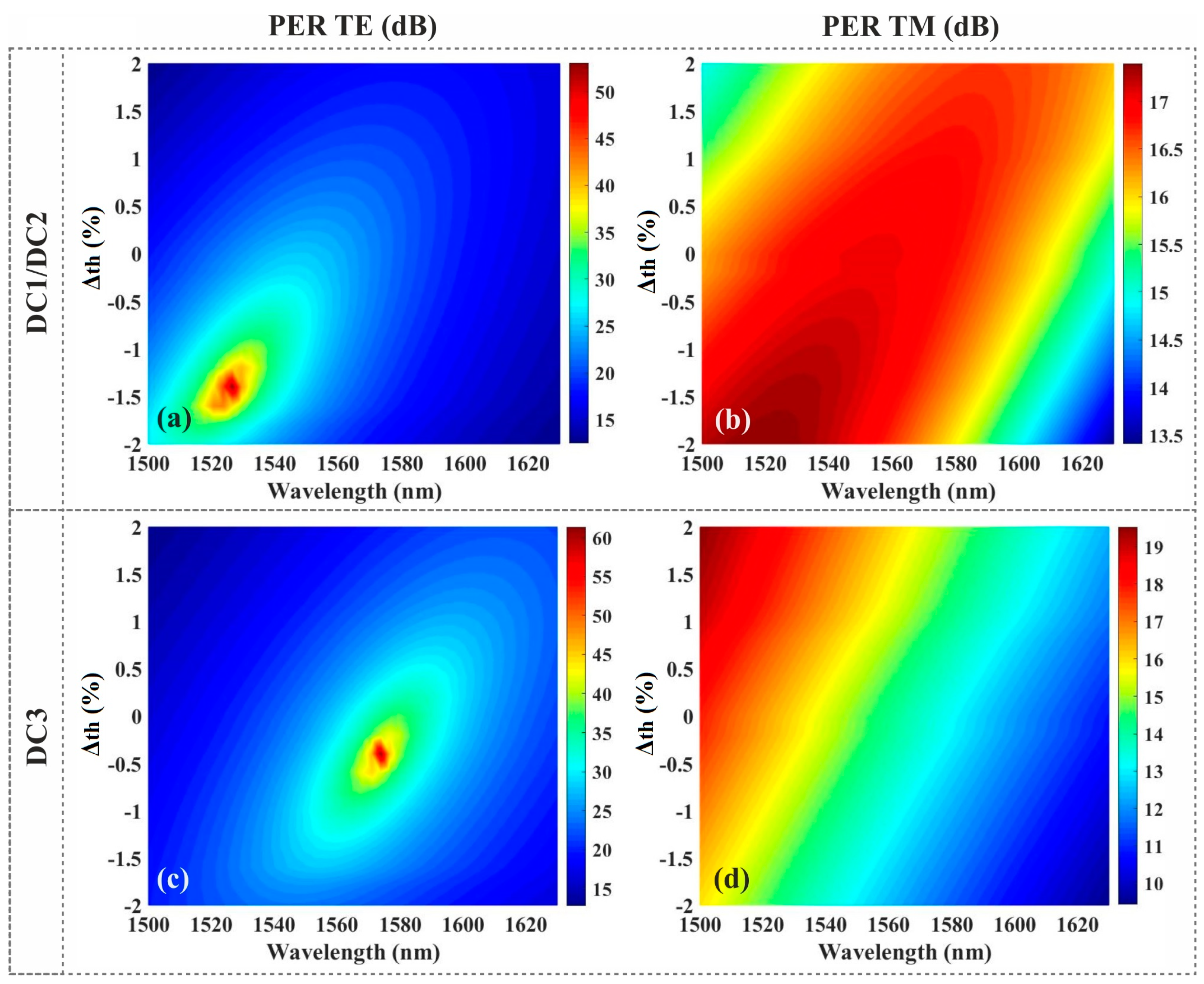
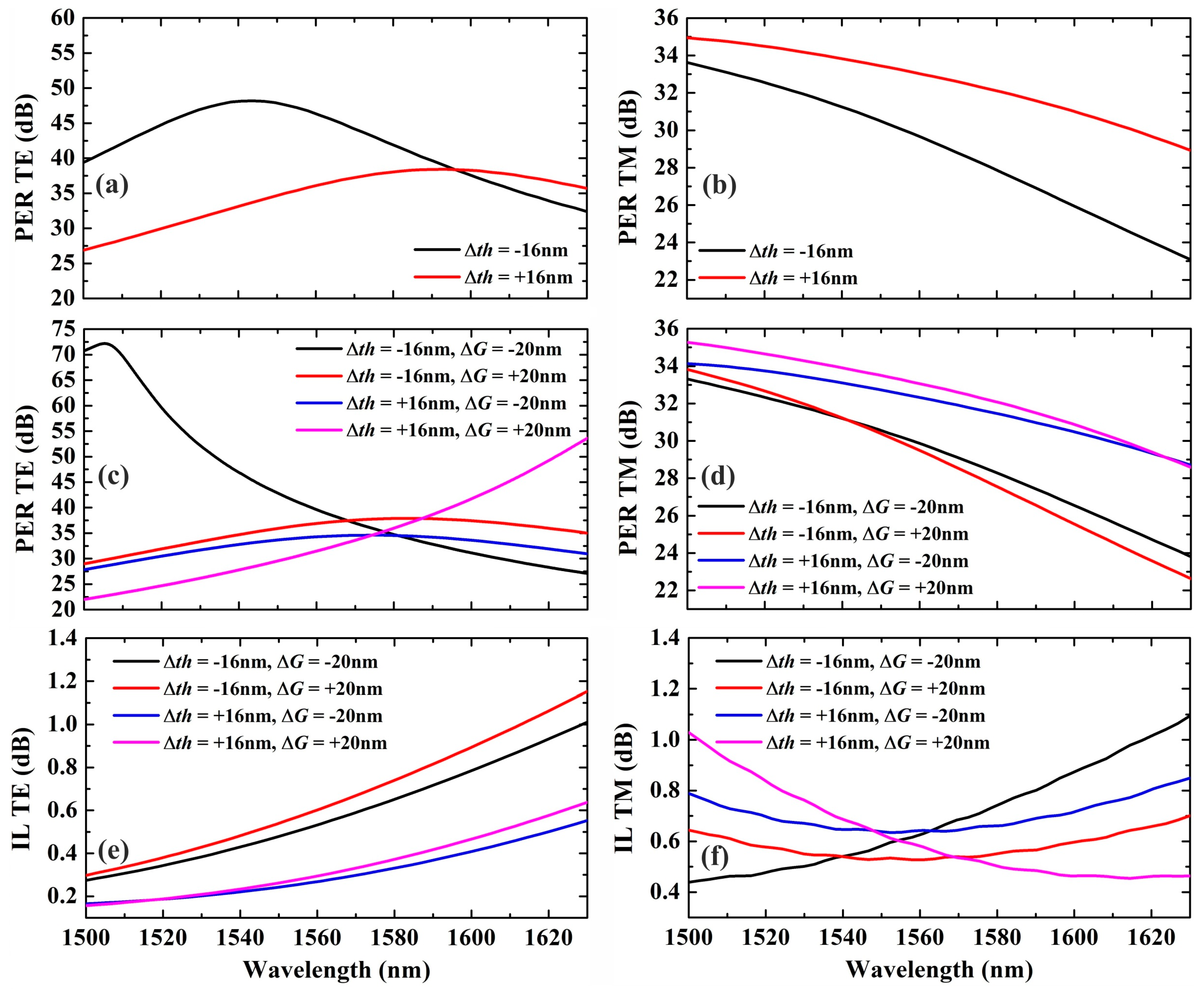
4. Fabrication Tolerance Analysis

Taking into consideration that DCs are very sensitive to fabrication variations, it is important to evaluate numerically the impact of deviations from the optimum geometry to the overall performance of the device. The fabrication tolerance is initially investigated by simultaneously varying the thickness of both types of waveguides, Δth, for DC1/DC2 and DC3 by ±16 nm with a step of ±2 nm. The next step is to change the gap G by ±20 nm for Δth = ±16 nm, so as to identify which parameters affects mostly the PER of the proposed PBS. The other crucial parameter for the DC mechanism that is the form (gap, sidewalls) of the slot waveguide is not considered a variable for this tolerance analysis, as for a complete investigation three different parameters should be varied: the gap g and the width of two side walls, where their interplay affects the total width and form of the slot waveguide, rendering this task extremely complex.
The effect of the simultaneous variation of thickness, Δth, at both types of waveguides on PERTE and PERTM for a single DC is depicted in Figure 8. According to Figure 8a,b for DC1/DC2, minimum PERΤΕ ranges between 12.3 dB and 12.7 dB at the edges of the wavelength range, while minimum PERΤΜ is between 13.4 dB and 14.9 dB. Also Figure 8c,d shows that for DC3 the minimum PERTE ranges between 12.8 dB and 16.5 dB at the edges of the wavelength range, while the minimum PERTM is between 9.5 dB and 12.4 dB. Overall, it is clear and in agreement from what was expected that deviations in thicknesses will result to a decline in efficiency of the DCs for TE or TM polarization, or both, therefore affecting the performance of the overall device.
Having calculated the performance degradation of the two DCs versus the variation of Δth, the next step is to proceed to the extraction of the worst-case scenario when G also deviates from its optimal value by ±20 nm with corresponding results presented in Figure 9. Figure 9a reveals that the deviation of the thicknesses by −16 nm or +16 nm leads to a minimum PERTE of 32.4 dB or 26.8 dB, respectively, while according to Figure 9b the PERTM minimum value is 23 dB for Δth of −16 nm and 28.9 dB for Δth +16 nm at the upper end of 1630 nm. Going now to the worst-case scenario where the gap G deviates also from its optimum value for Δth= ±16 nm, Figure 9c shows that minimum PERTE lies between 28.9 dB and 22 dB for all combinations with the worst one emerging for Δth = +16 nm and ΔG = +20 nm. From Figure 9d it is also evident that for TM polarization, minimum PERTM is 22.6 dB for the combination of Δth = −16 nm and ΔG = +20 nm with a clear trend for lower values as the operation wavelength increases. The comparison between Figure 9a,c and Figure 9b,d reveals that precise control of Δth is crucial in order to maintain very good wideband PER performance, especially for TM polarization. On the other hand, ΔG seems to have minor effect in the overall performance of the cascaded layout. Regarding the degradation of the IL from fabrication errors, according to Figure 9e,f TE light features a maximum value of ~ 1.2 dB for the worst case of Δth = −16 nm and ΔG = +20 nm, while TM does not exceed 1.1 dB, when Δth = −16 nm and ΔG = −20 nm, respectively. Comparing these results with the optimum design presented in Section 3, the minimum PERTE declines up to 12.3 dB and the PERTM up to 8 dB for these assumed worst-case scenarios, where both Δth are ΔG values are missed by the widest accepted margin in lithography, deposition and etching of the Si3N4 core layer. It should be noted that if a PER of 20 dB is considered acceptable, the proposed design has a 2 dB margin for even higher tolerance to fabrication errors. Also, if a maximum 1.5 dB theoretical value is considered acceptable for the IL, there is still space for relaxing even further the fabrication tightness coming with the DC sensitivity.

5. Discussion

In this section, the proposed design of this work is compared from every aspect with existing state-of-the-art Si3N4 PBSs reported in the literature. Table 2 summarizes the key performance metrics of seven Si3N4 PBS designs based on different techniques for direct performance comparison, where “S” refers to the simulated and “E” to the experimental values. The table also includes the number of etching steps required for the fabrication of each design, in order to take into account also the parameter of fabrication complexity. Even though the angled MMI-based PBS of [15] exhibits a slightly lower footprint, it has a minimum PER at least 12.6 dB lower than the one achieved in this work in combination with a 30 nm reduced bandwidth. In addition, the design of [16] exploiting a 2×2 MMI and anodized gratings features a very high PER of >30 dB and low IL, however this comes at the expense of bandwidth that is now only 22 nm, while the footprint is also six times larger. In [10] the operation bandwidth is 95 nm wide at the O-band by cascading phase-controlled DCs, while the minimum PER is 20 dB, but the IL and the footprint are quite higher. In [16] the layout is quite complex, as it is based on handling the first order TM mode from cascaded asymmetric DCs and achieves 80 nm wide operation at the expense of minimum PER, that is only 10 dB. The PBS in [25] is based on cascaded multimode interferometers with very good performance in terms of overall footprint, losses and operational range, but again the minimum PER is only 10 dB for 100 nm range. In [13] the polarization splitting is relying on a horizontal multi-slot waveguide demonstrating 100 nm bandwidth with more than 20 dB PER within a length of 286 μm. The downside of this design is that the specific cross section of the waveguide must be applied across the whole PIC, if only one etching step is used. Otherwise, two etching steps should be applied for the slot formation. Finally, the design of [17] requires two etching steps for the formation of the three-dimensional vertical directional coupler and achieves more than 16 dB PER over a 30 nm range with very low IL, but the overall footprint is quite large. The last row presents for comparison the key performance metrics of the proposed PBS design that is based on cascaded directional couplers with vertical slots, where superior performance in terms of PER, IL and footprint is exhibited across a very wide 130 nm wavelength span that covers the SCL-band. The separation of the two polarization states follows a similar design strategy exploited on SOI platform in [9], but here significant analysis and optimization in the layout is required, as the basic polarization discrimination mechanism is highly wavelength sensitive and also due to the fact that the effective refractive index of thick Si3N4 waveguides is almost identical for the TE and TM polarization. This exceptional performance is coming though at the expense of the higher fabrication complexity required by the two etching depths.

6. Conclusions

In this work, we propose a silicon nitride-based PBS layout that exploits a strip and a vertical slot waveguide, with different thicknesses to discriminate the fundamental modes of the TE and TM polarizations via directional coupling. The device is optimized through extensive FDE and 3D-FDTD electromagnetic simulations, so that the input TM polarized light is directionally coupled from the 470 nm thick strip to the 800 nm thick vertical slot waveguide, while the TE polarized light continues to propagate in the strip waveguide. The proposed PBS design manages to expand the operational window with a high PER for both polarizations, overcoming the inherent wavelength dependence of the directional coupling polarization discrimination mechanism. In the first stage of this analysis, the PBS is optimized for 1550 nm wavelength with maximum IL of 0.18 dB and a minimum PER of 15.4 dB for both polarizations across a 130 nm span at SCL-band. For further optimization of the broadband performance two PBS layouts were identified with variations in the critical parameters of gap G between the slot and strip waveguides and the coupling length Lc in the DC section, aiming for the highest attainable PER at the edges of the targeted window. In this way a cascaded network of two PBSs per polarization port, attains minimum values of 34.3 dB and 30.6 dB for PERTE and PERTM, respectively, a total footprint of 94 × 14 μm2 and IL lower than 0.8 dB for both polarizations. Finally, a fabrication tolerance analysis was performed taking as worst-case scenarios simultaneous deviations of Δth = ±16 nm from optimum thicknesses and ΔG = ±20 nm from optimum gap in the DCs. Under these non-optimum conditions, the minimum PERTE and PERTM are calculated above 22 dB, while the are IL below 1.2 dB in the entire 1500–1630 nm range. These results verify the resilience of the proposed design to provide PER values above the 20 dB benchmark without strict limitations in the fabrication process.

Author Contributions

G.P. wrote the paper and conducted the simulations and analysis, D.K. and D.C. aided in simulations and checked the paper, K.V. supervised. All authors have read and agreed to the published version of the manuscript.

Funding

This research received no external funding.

Institutional Review Board Statement

Not applicable.

Informed Consent Statement

Not applicable.

Data Availability Statement

All data generated during this work can be obtained from the corresponding author upon reasonable request.

Acknowledgments

We highly appreciate the support provided by the European H2020 ICT NEBULA (GA No. 871658) project.

Conflicts of Interest

The authors declare no conflict of interest.

References

  1. Siew, S.Y.; Li, B.; Gao, F.; Zheng, H.Y.; Zhang, W.; Guo, P.; Xie, S.W.; Song, A.; Dong, B.; Luo, L.W.; et al. Review of Silicon Photonics Technology and Platform Development. J. Lightwave Technol. 2021, 39, 4374–4389. [Google Scholar] [CrossRef]
  2. Chrostowski, L.; Hochberg, M. Silicon Photonics Design: From Devices to Systems; Cambridge University Press: Cambridge, UK, 2015. [Google Scholar]
  3. Muñoz, P.; Mico, G.; Bru, L.A.; Pastor, D.; Perez, D.; Domenech, J.D.; Fernandez, J.; Banos, R.; Gargallo, B.; Alemany, R.; et al. Silicon Nitride Photonic Integration Platforms for Visible, Near-Infrared and Mid-Infrared Applications. Sensors 2017, 17, 2088. [Google Scholar] [CrossRef]
  4. Asakawa, K.; Sugimoto, Y.; Nakamura, S. Silicon photonics for telecom and data-com applications. Opto-Electron. Adv. 2020, 3, 200011. [Google Scholar] [CrossRef]
  5. Heck, M. Highly integrated optical phased arrays: Photonic integrated circuits for optical beam shaping and beam steering. Nanophotonics 2017, 6, 93–107. [Google Scholar] [CrossRef]
  6. Morant, M.; Pérez, J.; Llorente, R. Polarization Division Multiplexing of OFDM Radio-over-Fiber Signals in Passive Optical Networks. Hindawi Adv. Opt. Technol. 2014, 2014, 269524. [Google Scholar] [CrossRef]
  7. Ivanovich, D.; Powel, S.B.; Gruev, V.; Chamberlain, R.D. Polarization division multiplexing for optical data communications. SPIE OPTO 2018, 15038, 160–178. [Google Scholar]
  8. Shahwar, D.; Cherchi, M.; Harjanne, M.; Kapulainen, M.; Aalto, T. Polarization splitters for micron-scale silicon photonics. Proc. SPIE 2021, 11691, 1169104. [Google Scholar]
  9. Tian, Y.; Qiu, J.; Liu, C.; Tian, S.; Huang, Z.; Wu, J. Compact polarization beam splitter with a high extinction ratio over S + C + L band. Opt. Express 2019, 27, 999–1009. [Google Scholar] [CrossRef]
  10. Guerber, S.; Ramos, C.A.; Benedikovic, D.; Valdeiglesias, E.D.; Le Roux, X.; Vulliet, N.; Cassan, E.; Morini, D.M.; Baudot, C.; Boeuf, F.; et al. Broadband Polarization Beam Splitter on a Silicon Nitride Platform for O-Band Operation. IEEE Photonics Technol. Lett. 2018, 30, 2679–2682. [Google Scholar] [CrossRef]
  11. Gao, S.; Wang, Y.; Wang, K.; Skafidas, E. Low-Loss and Broadband 2 × 2 Polarization Beam Splitter Based on Silicon Nitride Platform. IEEE Photonics Technol. Lett. 2016, 28, 1936–1939. [Google Scholar] [CrossRef]
  12. Jijun, F.; Ryoichi, A. Silicon nitride polarizing beam splitter with potential application for intersubband-transition-based all-optical gate device. Jpn. J. Appl. Phys. 2015, 54, 04DG08. [Google Scholar]
  13. Fang, Y.; Bao, C.; Wang, Z.; Liu, Y.; Zhang, L.; Huang, H.; Ren, Y.; Pan, Z. Polarization Beam Splitter Based on Si3N4/SiO2 Horizontal Slot Waveguides for On-Chip High-Power Applications. Sensors 2020, 20, 2862. [Google Scholar] [CrossRef] [PubMed]
  14. Jhan, J.; Brocj, J.; Veilleux, S.; Dagenais, M. Silicon nitride polarization beam splitter based on polarization-independent MMIs and apodized Bragg gratings. Opt. Express 2021, 29, 14476–14485. [Google Scholar]
  15. Kudalippalliyalil, R.; Murphy, T.E.; Grutter, K. Low-loss and ultra-broadband silicon nitride angled MMI polarization splitter/combiner. Opt. Express 2020, 28, 34111–34122. [Google Scholar] [CrossRef] [PubMed]
  16. Bhandari, B.; Im, C.-S.; Sapkota, O.R.; Lee, S.-S. Highly efficient broadband silicon nitride polarization beam splitter incorporating serially cascaded asymmetric directional couplers. Opt. Lett. 2020, 45, 5974–5977. [Google Scholar] [CrossRef]
  17. Feng, J.; Akimoto, R. A Three-Dimensional Silicon Nitride Polarizing Beam Splitter. IEEE Photonics Technol. Let. 2014, 26, 706–709. [Google Scholar] [CrossRef]
  18. Wilmart, Q.; El Dirani, H.; Tyler, N.; Fowler, D.; Malhouitre, S.; Garcia, S.; Casale, M.; Kerdiles, S.; Hassan, K.; Monat, C.; et al. A Versatile Silicon-Silicon Nireide Photonics Platform for Enhanced Functionalities and Applications. Appl. Sci. 2019, 9, 255. [Google Scholar] [CrossRef] [Green Version]
  19. El Dirani, H.; Youssef, L.; Petit-Etienne, C.; Kerdiles, S.; Grosse, P.; Monat, C.; Pargon, E.; Sciancalepore, C. Ultralow-loss tightly confining Si3N4 waveguides and high-Q microresonators. Opt. Express 2019, 21, 30726–30740. [Google Scholar] [CrossRef]
  20. Muñoz, P.; Pastor, D.; Bru, L.A.; Cabanes, G.M.; Benitez, J.; Goodwill, D.; Bernier, E. Scalable Switched Slab Coupler Based Optical Phased Array on Silicon Nitride. IEEE J. Sel. Top. Quantum Electron. 2021, 27, 1–16. [Google Scholar]
  21. Chatzitheocharis, D.; Ketzaki, D.; Calò, C.; Caillaud, C.; Vyrsokinos, K. Design of Si-rich nitride interposer waveguides for efficient light coupling from InP-based QD-emitters to Si3N4 waveguides on a silicon substrate. Opt. Express 2020, 28, 34219–34236. [Google Scholar] [CrossRef]
  22. Abouheaf, M.; Gueaieb, W.; Samra, A. Modeling of evanescent-wave coupling between optical dielectric waveguides. Int. J. Model. Simul. 2019, 39, 38–47. [Google Scholar] [CrossRef]
  23. Roeloffzen, C.G.H.; Hoekman, M.; Klein, E.J.; Wevers, L.S.; Timens, R.B.; Marchenko, D.; Geskus, D.; Dekker, R.; Alippi, A.; Grootjans, R.; et al. Low-Loss Si3-N4 TriPleX Optical Waveguides: Technology and Applications Overview. IEEE J. Sel. Top. Quantum Electron. 2018, 24, 1–21. [Google Scholar] [CrossRef] [Green Version]
  24. Chuang, S.L. Waveguide Couplers and Coupled-Mode Theory. In Physics of Optoelectronic Devices; Wiley-Interscience: New York, NY, USA, 1995; pp. 283–334. [Google Scholar]
  25. Tosi, M.; Fasciszewki, A.; Rossini, L.A.B.; Costanzo, P.A. Silicon nitride polarisation beam splitters: A review. IET Optoelectron. 2019, 14, 120–124. [Google Scholar] [CrossRef]
Figure 1. (a) Illustration of the proposed DC-based PBS layout consisting of the strip and slot waveguides. The blue arrow represents the TE polarization, and the red arrow the TM. (b) Cross sectional view of the waveguides in coupling region where polarization discrimination is achieved. (c) Modal profiles of the supported TE and TM modes in the strip and waveguide, respectively.
Photonics 09 00552 g001
Figure 2. Calculated effective refractive indices of the TE and TM modes and the respective Δneff at 1550 nm for the (a) slot waveguide with varying g and the (b) strip waveguide with varying t.
Photonics 09 00552 g002
Figure 3. (a) Calculated transmission of the TM mode versus Lc. (b) TE and TM mode wideband transmission for Lc = 10.3 μm. (c) Device PER for TE and TM polarization. Electric field distribution along the PBS for (d) TE and (e) TM input polarizations.
Photonics 09 00552 g003
Figure 4. Calculated PER of the (a) TE and (b) TM polarization when Lc varies between 9–11.5 μm.
Photonics 09 00552 g004
Figure 5. Calculated TE and TM PER when G varies between 280 nm and 320 nm for (a,b) Lc1 = 9 μm and (c,d) Lc2 = 11.5 μm, respectively.
Photonics 09 00552 g005
Figure 6. Two-stage cascaded formation employing three PBSs, DC1, DC2 and DC3 with selected Lc and G. An adiabatic rib taper is used for the transition from DC1 and DC2 and the ports that are not used as outputs are terminated, as shown in the insets.
Photonics 09 00552 g006
Figure 7. Calculated PER for TE and TM polarization of the (a) DC1 & DC2 and (b) DC3 devices. (c) Aggregated transmission and (d) PER at the TE and TM ports of the two-stage cascaded formation.
Photonics 09 00552 g007
Figure 8. Effect of the variation of thicknesses, Δth, on the TE and TM PER values for (a,b) DC1/DC2 and (c,d) DC3, respectively. Higher and lower Δth values result to a reduction of the minimum PER.
Photonics 09 00552 g008
Figure 9. Performance of the PBS cascaded configuration for (a) TE and (b) TM polarization when Δth deviates by ±16 nm. Corresponding performance curves for (c) TE and (d) TM polarization when Δth = ±16 nm and ΔG deviated by ±20 nm. IL curves for (e) TE and (f) TM polarization for the four worst-case combinations of Δth and ΔG.
Photonics 09 00552 g009
Table 1. Design parameters of the two DCs.
PBSLc (μm)G (nm)PERTE (dB)PERTM (dB)IL (dB)
Single DC1/DC211.5320>15>15.3<0.23
Single DC39280>16.3>10.7<0.22
Cascaded >34.3>30.6<0.80
Table 2. Comparison with other PBS designs.
Ref.Wavelength Range (nm)Bandwidth (nm)PER (dB)IL (dB)FootprintEtching StepsTechnique
[14]1539–156122>30 (S&E)<1.1 (S&E)820 × 10 μm212×2 MMI and apodized grating
[10]1260–135595>20 (S&E)<1.3 (S&E)240 × 24 μm21phase-controlled cascaded DCs
[16]1520–160080>10 (S&E)<2.1 (S&E)113 μm long1cascaded asymmetric DCs
[25]1500–1600100>10 (S)<1 (S)400 × 10 μm21cascaded MMI
[13]1500–1600100<20 (S)-281 μm long1 or 2horizontal multi-slot waveguides
[17]1535–156530>16 (E)<1 (E)800 × 20 μm223D vertical directional coupler
this work1500–1630130>30.6 (S)<0.8 (S)94 × 14 μm22cascaded DCs with vertical slots
Publisher’s Note: MDPI stays neutral with regard to jurisdictional claims in published maps and institutional affiliations.

