1. Introduction
Photonic integrated circuits (PICs) can provide larger bandwidths, lower power consumption, immunity to the electromagnetic interference, etc., making them promising alternatives to their electronic counterparts in, for example, chip-scale interconnecting or sensing [
1]. Resembling the Moore’s Law in microelectronics, the integration density of PICs is doubling approximately every two years as well [
2], which inevitably requires the waveguides to be increasingly compact. To meet this, plasmonic waveguides have been developed to confine light in a scale that is even smaller than the diffraction limit. Indeed, they have already been playing vital roles in applications ranging from nonlinear optical signal processing [
3], light generation [
4] and optical sensing [
5] to quantum information processing [
6]. To date, varieties of plasmonic waveguides have been demonstrated, including the dielectric-loaded surface plasmon polariton waveguide (DLSPPW) [
7]; the long-range surface plasmon polariton waveguide (LRSPPW) [
8]; the channel plasmon polariton waveguide (CPPW) [
9]; and the hybrid plasmonic waveguide (HPW) [
10]. Principally, a trade-off always exists between the confinement capability and the propagation loss of a plasmonic waveguide, that light being more strongly bounded by the metal could produce smaller waveguides and devices whereas compromises the waveguide losses due to the increased metal absorption. Fortunately, HPWs may tremendously mitigate this trade-off by partially confining the light through the large index contrast between two lossless dielectrics rather than all by the plasmon polaritons. Therefore, HPWs are extensively used as basic components for modulators [
11], sensors [
12], etc. Typical structures are, but not limited to, the silver (Ag)-magnesium fluoride (MgF
2)-cadmium sulfide (CdS) structure with the metal on the bottom [
13] and the gold (Au)-silica (SiO
2)-silicon (Si) structure with the metal on the top [
14], which have been experimentally demonstrated.
In order to explore the scalable implementations of the HPWs and components, fiber coupling is seen to be indispensable. Currently, there are two coupling schemes for coupling light between a fiber and an on-chip waveguide, i.e., edge coupling [
15,
16] and surface coupling assisted by a grating coupler [
17,
18,
19,
20]. In practice, edge coupling restrains the position flexibility of the HPW-based components for approximating the edges is necessary and otherwise much light would be absorbed in the plasmonic waveguide connectors. Meanwhile, it also needs complicated fabrication processes such as facet polishing. In contrast, not only can grating couplers be placed anywhere on a chip to allow chip scale testing, but they do not need facet polishing. Tremendous efforts have been paid to the optimization of the grating couplers [
21] and an apodized one, for example, could achieve a coupling efficiency (CE) as high as 81.3% [
22] between the standard single-mode fiber and a silicon waveguide.
However, to the best of our knowledge, no grating couplers for light coupling between the standard single-mode fiber and the HPWs have been reported yet. Former works usually coupled the fiber mode first to a dielectric mode and then converted it to the HPW mode. One exception is the work by Lou et al., where a fiber tip was used to directly couple light into the HPWs positioned in the middle of a chip [
23]. The use of a fiber tip is not friendly to packaging. Structures for coupling a dielectric mode to the HPW mode could be the plasmonic waveguide taper [
24], the polarization rotation and coupling (PRC) structure [
25] and the air-slot coupler [
26]. These indirect coupling methods involve complex structures and may need extra alignment processes in the fabrication. More significantly, they introduce additional insertion losses, limiting the total CE to be smaller than 63.4%. Here, we consider the highest CE between a dielectric waveguide and a HPW to be 78% [
25] and the highest CE between a fiber and a dielectric waveguide to be 81.3% [
22]. Note that by adding bottom reflectors [
27,
28], a polysilicon overlay [
29] or a binary blazed structure [
30] or by using slanted etching [
31], CEs between the fiber and the dielectric waveguides can be further promoted. However, the compromise is the increasing complication of the fabrication.
Here, for the first time, we propose grating couplers for direct coupling between a standard single-mode fiber and the silicon HPWs. In principle, such grating couplers can be used for any HPW, but here we choose the silicon HPWs as an example, since silicon-based waveguides exhibit the potentials in compatibility with the scalable CMOS manufacturing [
32]. Apodized grating couplers are designed for different kinds of silicon HPWs with a bottom metal layer or a metal cap, and they all simultaneously exhibit large CEs and large bandwidths. Moreover, a two-stage-taper mode converter is introduced to further promote the CEs. A remarkable CE of 79% and a 3-dB bandwidth of 73 nm between the fiber and the HPW as narrow as 100 nm is theoretically achieved.
2. Grating Couplers for the Silicon HPWs with a Bottom Metal Layer
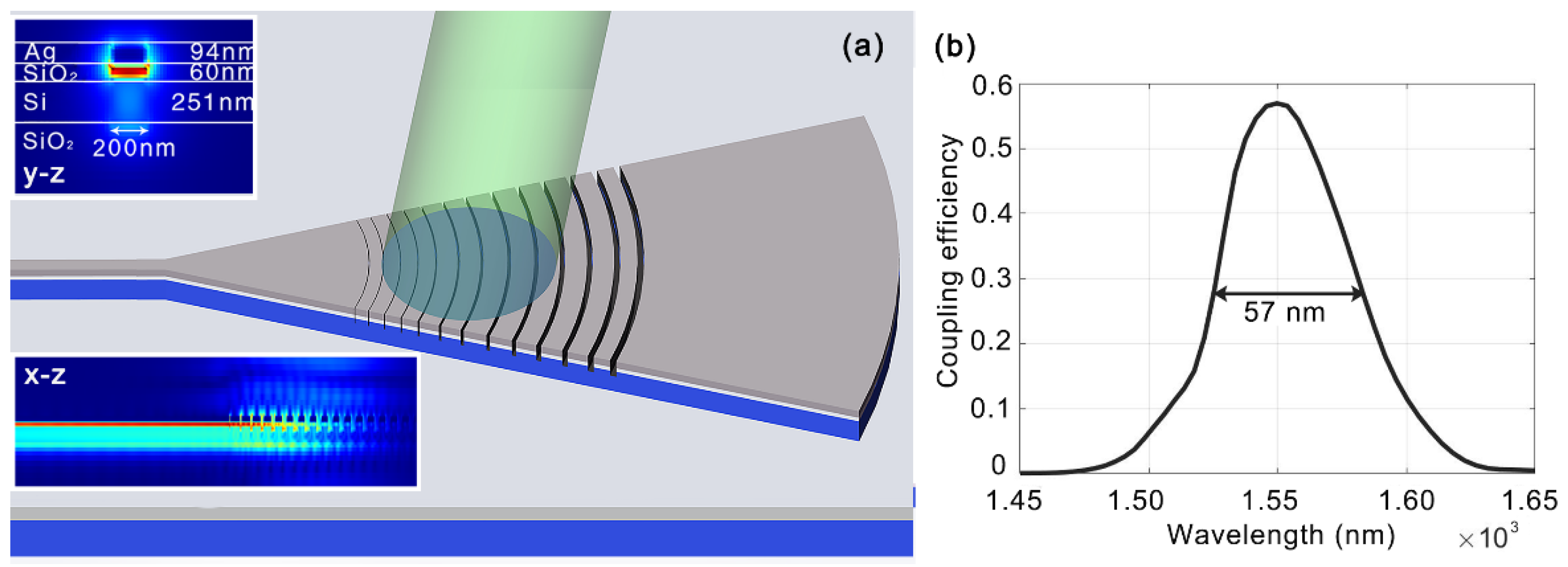
We first consider the silicon HPWs with a bottom metal layer. As can be seen in
Figure 1, the waveguide consists of four layers, i.e., a Si substrate, a bottom Ag layer, a thin intermediate SiO
2 layer and a top Si layer. Besides, the top cladding is SiO
2 for the waveguide investigated here and in the followings as well. The intermediate SiO
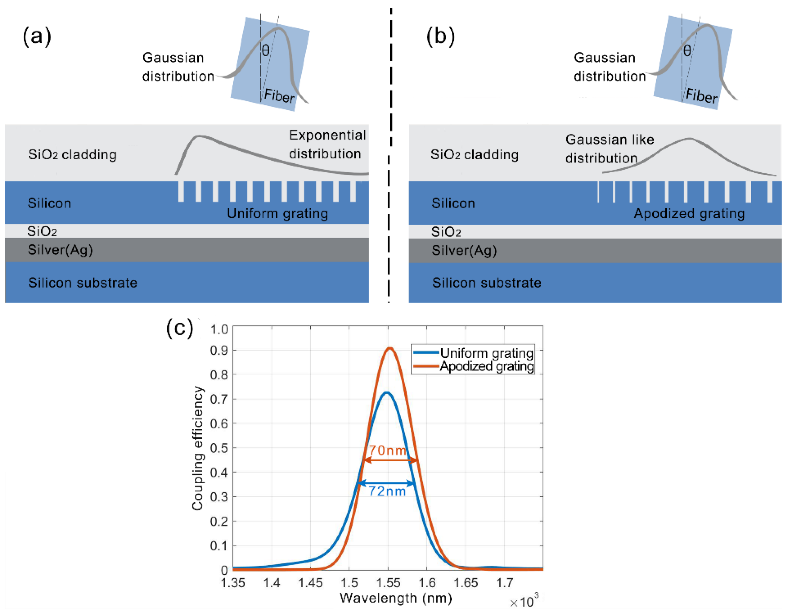
2 layer is thin enough (e.g., 10 s of nanometers) to allow the dielectric mode and the SPP mode to hybridize to form the hybrid plasmonic mode. The grating couplers are inscribed in the top Si layer. Hence, the Ag layer is not only involved in the formation of the hybrid plasmonic mode, but also behaves as a perfect bottom reflector to (almost) completely suppress the transmission towards the substrate. Uniform grating couplers are first designed as a starting point and then apodized grating couplers are implemented to improve the performances, with their 2D schematics shown in
Figure 1a,b, respectively.
Similar to the design of a grating coupler for the silicon dielectric waveguides [
33], the design of a grating coupler for the silicon HPWs also predominantly involves the optimization of the etching depth, the period and the duty cycle (i.e., tooth width/period) of the grating. A 2D finite-difference time-domain (FDTD, Ansys Inc, Canonsburg, PA, USA.) method is used to simulate the grating couplers with different combinations of structural parameters and a particle swarm optimization (PSO) algorithm [
34] is applied to search the best combination to achieve the highest CE at 1550 nm. In the optimizations, we fix the thicknesses of the SiO
2 cladding layer, Si core layer, thin SiO
2 layer and the Ag layer to be 1000 nm, 320 nm, 95 nm and 100 nm, respectively, and the tilt angle
θ of the fiber is fixed at 10°. Hereinafter, the refractive indices (RIs) at 1550 nm used for Si, SiO
2 and Ag are 3.478, 1.445 and 0.1453 + 11.3587i, respectively, the background material is set to be SiO
2, and the fundamental transverse-magnetic (TM
0) mode is considered. Meanwhile, the positions of the optical fiber have also been swept to ensure maximal CEs, and the left side of the fiber core is 600 nm away from the gratings in the vertical direction and 200 nm away from the leftmost groove in the horizontal direction, respectively. Finally, for the uniform grating coupler, a combination of the etching depth of 167 nm, the period of 725 nm and the duty cycle of 0.8 gives a CE of 73% at 1550 nm and a 3-dB bandwidth of 72 nm, as extracted from the transmission spectrum (blue line) in
Figure 1c.
Next, apodized grating couplers are designed for they have been proved to be able to alleviate the backscattering and improve the directionality and, more importantly, raise the profile match between the light distribution diffracted by the grating coupler and the Gaussian distribution of the fiber mode [
35]. This can be realized by gradually varying the etching depth of each groove [
36] or by incrementally changing the groove width, i.e., decreasing the duty cycle along the grating length [
37]. Since variation of the etching depths considerably challenges the fabrication, here, we implement the scheme of duty cycle variation. The duty cycles can be engineered in the form of a rising cosine wave [
38], simply in a linear form [
22] or determined by optimization algorithms [
35]. We tried these different methods and found that the differences among the eventually obtained optimal CEs were smaller than 3%. Thus, the simplest linear one is adopted for the apodized grating couplers for the silicon HPWs as it can pronouncedly mitigate the design and the manufacturing demands. The duty cycle, denoted as
f, is linearly tailored at a step of −0.02 and the grating period
P is correspondingly tuned to make sure every pair of tooth and groove satisfies the Bragg condition [
39]. Hence, the period variation, Δ
P, can be described as [
40]
where,
is the effective RI of some pair of the tooth and groove [
41] and
neff’ is the effective RI of the following pair.
n1 and
n2 represent the RIs of the tooth material (Si) and the groove material (SiO
2), respectively. We set the etching depth to be 167 nm, the same as that of the uniform one since the difference of the optimal etching depth is not significant, and optimize the starting values of
P and
f. Finally, a CE of 91% at 1550 nm and a 3-dB bandwidth of 70 nm can be accomplished when
fs of the first 10 pairs linearly change from 0.98 to 0.8 at a step of −0.02 and keep constant at 0.78 in the following 15 pairs, and
Ps of the first 10 periods change from 654 nm to 695 nm and keep constant at 700 nm in the following 15 pairs. The red line in
Figure 1c shows the transmission spectrum of the optimized apodized grating coupler, and one can find that he CE pronouncedly exceeds that of the uniform one in spite of a very slight compromise on the bandwidth.
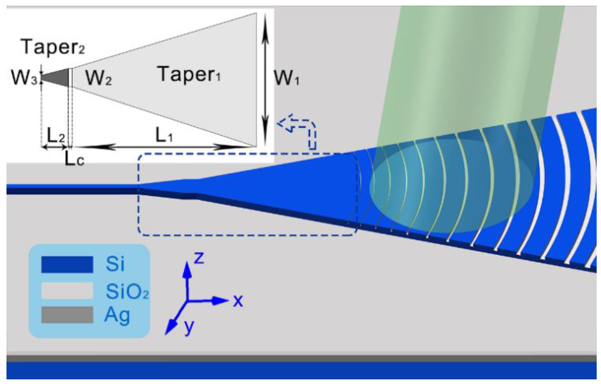
Then, we design and simulate the 3D structure of the apodized grating couplers for the silicon HPWs. The entire structure is schematically illustrated in
Figure 2, and it includes a focusing grating coupler, a mode converter consisting of a two-stage-taper and the silicon HPW that light is finally coupled into. The structural parameters of the gratings themselves are set according to the optimal parameters obtained from the 2D simulations. Focusing gratings are used here to compress the transmission region from the wide gratings to the narrow waveguide, which not only results in a more compact device but, what’s more, reduces the propagation loss by decreasing the length of the overall plasmonic waveguide region. To fully exploit the strong confinement of the silicon HPWs, the waveguide width can be as small as 100 nm. This imposes challenges on converting the light, which distributes in a 10 µm scale in the gratings to such a small waveguide since higher-order modes can be easily inspired and then leak or interfere with the fundamental mode in the tapered waveguide. To avoid this, we introduce a two-stage-taper (in the dashed line frame in
Figure 2) to accomplish the adiabatic mode converting.
The two-stage-taper mode converter consists of two trapezoidal tapers and a rectangle connector, with the taper widths denoted as
W1,
W2 and
W3, the length of the first taper
L1, the length of the second taper
L2 and the length of the connector
Lc.
W1 (=7.5 µm) is actually the width of the innermost tooth of the grating. Using the 3D FDTD simulation, we first investigate the one-stage-taper scheme, i.e., calculate the CEs of the fiber mode to the TM
0 mode of a waveguide with the width
W2, and the results are shown in
Figure 3a. Here, for each
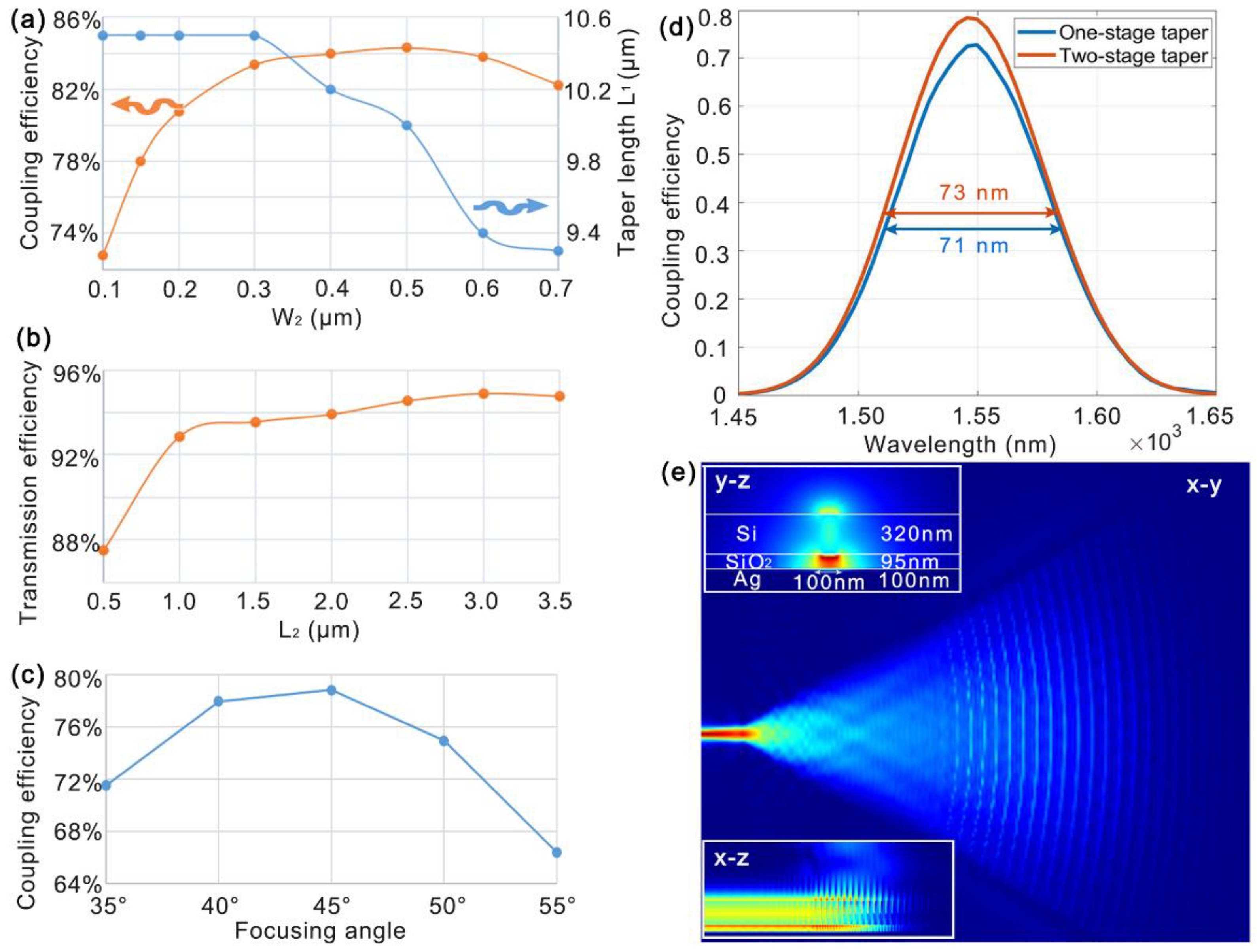
W2,
L1 has been optimized to attain the maximal CE. Interestingly, a peak value of ~84.3% appears at
W2 = 500 nm. This can be attributed to that, mode conversion to a very narrow waveguide involves a very long and narrow part of a taper and, thus, introduces a great loss, while conversion to a very wide waveguide easily inspires higher-order modes and suggests additional losses as well. Meanwhile, a different waveguide width may require a different focusing angle to achieve the best coupling. We then set
W2 to be 500 nm and vary
L2 to calculate the transmission efficiencies of the second taper itself, i.e., CEs from the TM
0 mode of the 500 nm-wide silicon HPW to that of the 100 nm-wide one. The transmission efficiency attains the maximum of ~94.9% at
L2 = 3 µm, as shown in
Figure 3b. We then explore how the focusing angle influences the CEs when
W2 = 500 nm and
L2 = 3 µm, as the curve in
Figure 3c shows. A maximum value of 79% of the CE happens at the focusing angle of 45° and larger or smaller angles will degrade the efficiencies a lot. This can be attributed to that the inappropriate angles would inspire higher order modes or introduce additional losses.
Figure 3d shows the overall transmission spectra from the fiber to the 100 nm-wide silicon HPW via the one-stage-taper (blue line) and the two-stage-taper (red line). Here, for the two-stage-taper,
Lc is 500 nm. CEs at 1550 nm are 73% and 79%, with the two-stage scheme being 6% higher and having a little improvement on the 3-dB bandwidth (73 nm vs. 71 nm).
Figure 3e shows the light propagation (x-y plane) from the gratings to the waveguide via the two-stage-taper and the upper inset exhibits the mode profile (y-z plane) in the 100 nm-wide waveguide, while the lower inset presents the light propagation in the x-z plane. One can find light is focused into the waveguide in a short length and the field is strongly enhanced in the SiO
2 nanolayer, resulting in a small mode area of 0.2668 µm
2.
3. Grating Couplers for the Silicon HPWs with a Metal Cap
The silicon HPWs with the metal layer on the bottom may not adapt to all applications since, from the perspective of fabrication, the top Si layer has to be fabricated by deposition or by using a flip-chip bonding process. The deposition method gives an amorphous Si layer which presents the instability issue after a high light power input [
42,
43] and the bonding method includes complex processes [
44]. Therefore, we next consider the silicon HPWs with a metal cap on the commonly used silicon-on-insulator (SOI) base [
45] and design grating couplers for them.
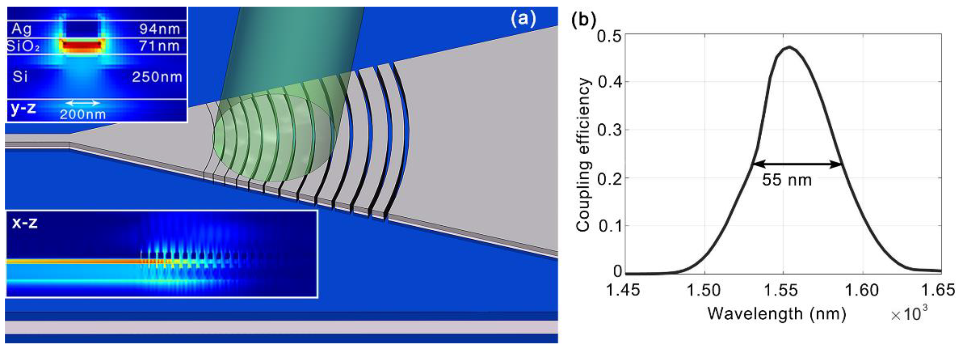
Figure 4a depicts the first waveguide structure, in which a Si-SiO
2-Ag stripe waveguide sits on a SiO
2 insulator layer. The upper inset shows the mode profile (y-z plane) of such a waveguide with the width of 200 nm at the 1550 nm wavelength and the lower inset presents the light propagation (x-z plane). Since Si, SiO
2 and Ag layers all possess nanostructures, light can be tightly confined in the waveguide, giving an effective mode area of 0.1291 µm
2.
Similar design methods and simulation processes as that described in the last section are implemented to optimize the apodized grating couplers for this sort of silicon HPW. Thicknesses of the layers used here are 250 nm for the Si layer, 60 nm for the SiO
2 layer and 94 nm for the Ag cap. An optimal grating structure is obtained when the periods/duty cycles of the first six apodized pairs of teeth and grooves are 707 nm/0.95, 717 nm/0.86, 729 nm/0.78, 744 nm/0.71, 762 nm/0.65, 784 nm/0.59 and that of the following fifteen uniform pairs are 810 nm/0.55. For the grooves, the 60-nm thick SiO
2 layer is etched through and the Si layer is etched by 68 nm. Meanwhile, the groove widths change from 35 nm (the innermost) to 365 nm (the outermost). We also tried the two-stage-taper mode converter for this sort of waveguides, but the improvement was not pronounced (<1%). Hence, we directly implemented the one-stage-taper.
Figure 4b shows the simulated transmission spectrum from the fiber to a 200 nm-wide silicon HPW. A peak CE of 57% at 1550 nm and a 3-dB bandwidth of 57 nm are extracted. Without the metal layer playing as a bottom reflector, the CE degrades a lot compared to that for the silicon HPW with a bottom metal layer.
As a guidance for the fabrication of the above investigated silicon HPWs with a metal cap and the grating couplers, we illustrate the fabrication processes in
Figure 5. First, the Ag structures are patterned on the SOI wafer through a lithography and a lift-off process, as depicted by
Figure 5a, the y-z cross-section view of the waveguide and
Figure 5d, the x-z cross-section view of the grating coupler. Then, with the Ag structures acting as the hard mask, the SiO
2 nanolayer is etched through and the Si layer is partially etched to the depth of the grooves of the grating coupler using a reactive-ion etching (RIE) process.
Figure 5b,e show the two cross-section views respectively. Finally, using a second lithography to only cover the grating couplers with resists and a following RIE process, all the Si slabs exposed to the ions are etched through to form the stripe silicon HPW, as shown by the two cross-section views in
Figure 5c,f. After residual resist stripping, the waveguides are finalized by a SiO
2 cladding deposition.
Some devices may need to sustain the Si slab in the silicon HPWs, such as the electro-optic modulator with a slab as the carrier injection region or the suspended devices possessing a slab as the support. Therefore, we design the grating couplers for the silicon HPWs with a Si slab. Meanwhile, to pattern the waveguide and the grating couplers through one etching step to simplify the future fabrication, the waveguide and the coupler having the same etching depths are considered.
Figure 6a depicts the 3D schematic of the entire structure and the upper inset shows the mode profile (y-z plane) of a 200 nm-wide waveguide with the effective mode area calculated to be 0.1412 µm
2, while the lower inset presents the light propagation (x-z plane). The thicknesses used here are 250 nm for the total Si layer, 71 nm for the SiO
2 nanolayer and 94 nm for the Ag cap. The thicknesses of the Si slab and the Si rib of the waveguide are 182 nm and 68 nm, respectively. Using the 3D FDTD simulation method and the PSO algorithm, the optimal grating coupler structure is obtained when the periods/duty cycles of the first six apodized pairs of teeth and grooves are 700 nm/0.95, 710 nm/0.86, 722 nm/0.78, 736 nm/0.71, 754 nm/0.65, 776 nm/0.59 and that of the following fifteen uniform pairs are 802 nm/0.548.
Figure 6b shows the simulated transmission spectrum from the fiber to the 200 nm-wide waveguide and a peak CE of 47% and a 3-dB bandwidth of 55 nm are achieved.
One fundamental character of a plasmonic waveguide is that light can be tightly bounded by the plasmon polaritons and propagates along the metal surface, suggesting that Si or SiO
2 nanostructures may not be necessary to confine the light. Thus, as the entire structure in
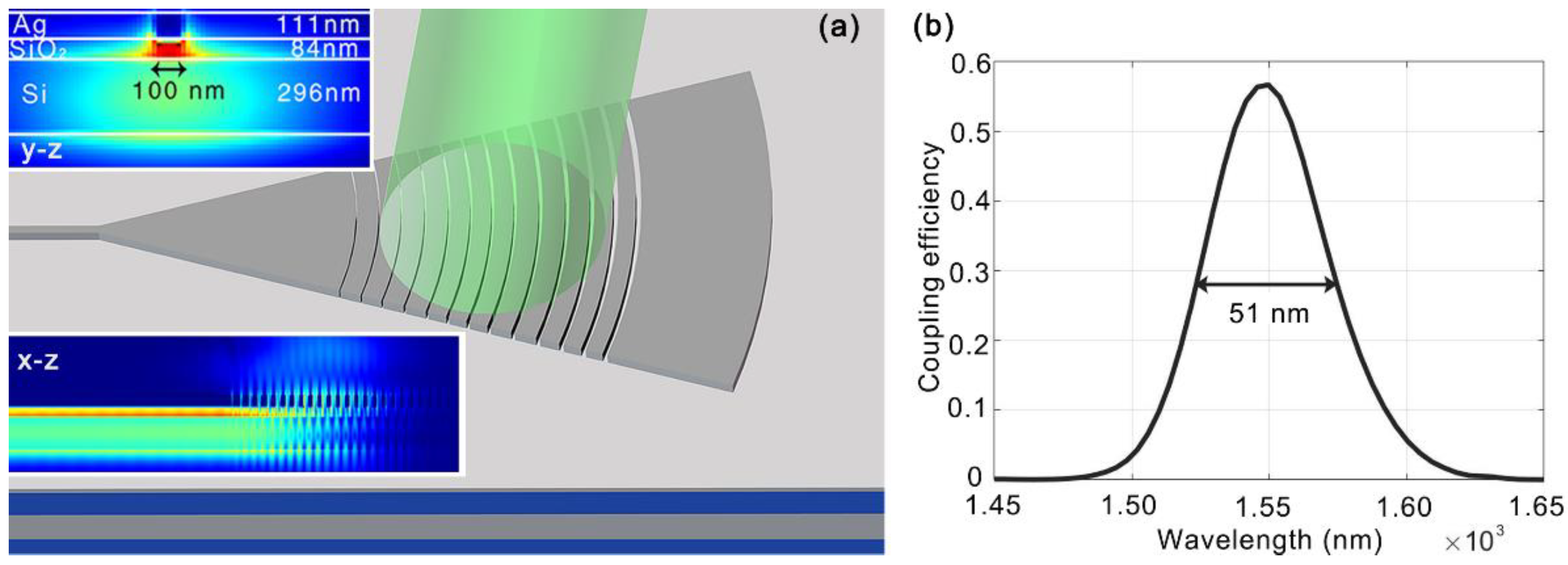
Figure 7a shows, we further consider the silicon HPWs without etching the Si or SiO
2 layers, but with the waveguides being defined only by the Ag caps, and design the grating couplers for this sort of waveguides. The fabrication of such a waveguide is expected to be very simple since no etching processes but only a lithography and a metal liftoff process are needed. The thicknesses used here are 296 nm for the Si layer, 84 nm for the SiO
2 layer and 111 nm for the Ag cap. These thicknesses are chosen by taking the layer thicknesses into consideration during the optimizations. One can of course choose other layer thicknesses but may obtain a slightly lower optimal CE. The upper inset of
Figure 7a shows the mode profile of a 100-wide waveguide while the lower exhibits the light propagation (x-z plane) from the grating coupler to the waveguide. One can find that much light distributes in the Si layer, giving a large effective mode area of 0.5396 µm
2. Nevertheless, the mode still has an enhancement in the SiO
2 nanolayer under the Ag cap, not completely compromising the profits introduced by the “hybrid” scheme. With simulations and optimizations, the optimal grating coupler structure is obtained when the periods/duty cycles of the first five apodized pairs of teeth and grooves are 622 nm/0.89, 625 nm/0.81, 629 nm/0.74, 633 nm/0.67, 637 nm/0.6, and that of the following fifteen uniform pairs are 641 nm/0.53.
Figure 7b shows the simulated transmission spectrum from the fiber to the 100 nm-wide silicon HPW and a peak CE of 57% and a 3-dB bandwidth of 51 nm are achieved.
4. Discussion
To better understand the proposed coupling scheme and further improve the coupling efficiency, we investigated the various origins of the coupling losses and their take-ups in the total loss. For the uniform grating coupler with a bottom metal layer, the proportions of back scattering, top reflection, metal absorption, loss from generation of other modes, and the mismatch between a fiber mode and the mode scattered by the gratings are 0.3%, 17.4%, 12.9%, 1.9%, and 4.8%, respectively. Meanwhile, for the apodized grating coupler with a bottom metal layer, these proportions are 0.2%, 6.5%, 12.9%, 1.5%, and 0.4%. Apparently, the apodization scheme reduces the mode mismatch and improves directionality. For both schemes, the predominant loss source is the metal absorption and one may use a thicker intermediate layer to reduce the loss of such. But the sacrifice is a decreased confinement of the HPW. As for the apodized grating couplers for the HPWs with a metal cap, e.g., the one with a Si stripe, proportions of the abovementioned losses are 0.1%, 20.2%, 15.1%, 2.5%, and 0.3%, respectively. In comparison, the loss of top reflection is much larger due to the reflection of the top metal cap, and there is about a 5.5% loss of the bottom scattering since no bottom metal layer presents.
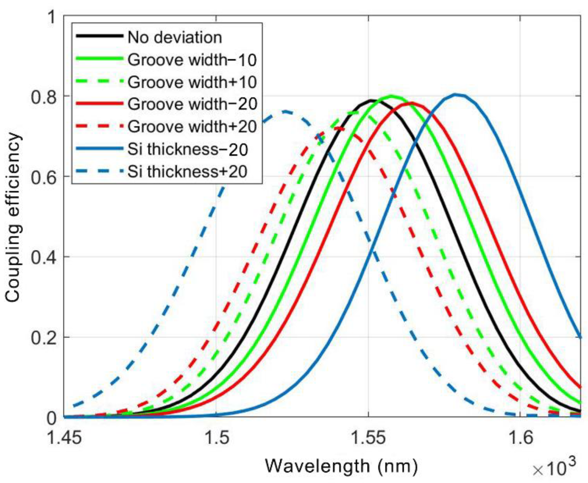
It is well known that the performances of a grating coupler for the silicon dielectric waveguide can be degraded by the fabrication deviations from the optimal designs. Here, we take the silicon HPWs with a bottom metal layer as an example and analyze how the fabrication deviations affect the coupling efficiencies of the proposed apodized grating couplers for these HPWs, as shown in
Figure 8. The black solid line, which is extracted from
Figure 3d, indicates the CEs for couplers with the optimal dimensions. Green curves and red curves show the simulated CEs of the couplers with ±10 nm and ±20 nm deviations from the originally designed groove widths, respectively. Degradations inevitably happen but are smaller than 12% even at the ±20 nm deviations. Considering the modern nano-fabrication technologies are capable of controlling the deviations to ±10 nm, the degradations of the CEs at 1550 nm can be as small as <4%, thanks to the large bandwidths of the proposed grating couplers.
However, resembling that for the silicon dielectric waveguides, the grating coupler performances have pronounced dependences on the silicon layer thickness for the silicon HPWs. The blue curves in
Figure 8 point out such dependences and ±20 nm deviations of the silicon layer thickness can shift the center wavelength by 30 nm and degrade the CEs at the 1550 nm wavelength by ~3 dB. Thus, it is key to accurately control the deposition of the top silicon layer, which may be achieved using high-resolution in-situ monitoring methods. Furthermore, we change the etching depths by ±20 nm and find a negligible shift of the center wavelengths but a small degradation of ~6% of the CEs at 1550 nm. To extract more information of the fabrication tolerances of the proposed grating couplers, we use the 2D FDTD method and change the thicknesses of the thin SiO
2 intermediate layer by ±10 nm. The maximal CEs of 92% at 1543 nm (+10 nm) and 90% at 1555 nm (−10 nm) are obtained. What’s more, the deviations of the thicknesses of the SiO
2 cladding layer have almost no influences on the peak values of CEs, but cause the shift of the center wavelengths, e.g., the central wavelength is at 1540 nm when the thickness of the SiO
2 cladding layer is changed by −400 nm and at 1565 nm for a value of +400 nm. This can be rectified by adjusting the fiber tilt angle.
The fabrication tolerances of the grating couplers for the other three sorts of HPWs proposed in
Section 3 have also been analyzed. They are generally very sensitive to the Si thickness. For example, grating couplers for the waveguide with a Si stripe and a Ag cap can shift the center wavelength from 1550 nm to 1600 nm (+20 nm) and 1493 nm (−20 nm) with slight degradations of ~7% of the peak CEs. The influences of the deviations of the groove widths, the etching depths and the thicknesses of the SiO
2 intermediate layer are similar to that for the waveguides with a bottom metal layer.
Table 1 summarizes the overall performances of different sorts of silicon HPWs and the corresponding grating couplers that are investigated in this work. The performances of such for the indirect coupling scheme proposed by Song et al. [
24] are also listed for comparison. In the indirect coupling, a plasmonic taper was used to couple the silicon waveguide dielectric mode to the mode of a 200 nm-wide silicon HPW and the CE was 70%. Assuming a CE of 81.3% from the fiber to the silicon waveguide via a grating coupler, the total CE is less than 57%. This is comparable to that of the grating couplers for the silicon HPWs with a metal cap studied in this work, where CEs and bandwidths are around 50% and 55 nm, respectively. As elaborated in the introduction section, the trade-off between the confinement capability and the loss is always present. For example, the waveguide with a Ag cap on the SOI and no etch to the SOI exhibits a much smaller loss, but pronouncedly compromises the confinement. However, considering the tremendously simplified fabrication processes, this structure may draw special attention from a practical point of view. For the silicon HPWs with a bottom metal layer, the CE can be as high as 79%, impending the best CEs of the grating couplers for the silicon dielectric waveguides. Taking into account the relatively small waveguide loss, high confinement and moderately simple fabrication process, i.e., only once commonly used Si etching is needed, this kind of hybrid plasmonic waveguide structure should play more prominent roles in the future.

 ,
, 


