Article

High-Power, High-Efficiency Red Laser Diode Structures Grown on GaAs and GaAsP Metamorphic Superlattices

1
DRS Daylight Solutions, 1832 Wright St., Madison, WI 53704, USA
2
Department of Electrical and Computer Engineering, University of Wisconsin-Madison, 1415 Engineering Dr., Madison, WI 53706, USA
*
Author to whom correspondence should be addressed.
Photonics 2022, 9(7), 436; https://doi.org/10.3390/photonics9070436
Submission received: 27 May 2022 / Revised: 11 June 2022 / Accepted: 17 June 2022 / Published: 21 June 2022
(This article belongs to the Topic Optical and Optoelectronic Materials and Applications)

Abstract

:
Three types of GaAsP metamorphic buffer layers, including linearly graded, step graded, and metamorphic superlattices, were compared for the purposes of virtual substrates for red laser diode heterostructures. Laser diodes were fabricated on GaAs substrates and relaxed GaAsP metamorphic superlattice virtual substrates. A laser diode structure with a tensile-strained quantum well on a standard miscut GaAs substrate achieved TM-polarized emission at a 638 nm wavelength with 45% peak power conversion efficiency (PCE) at a 880 mW continuous wave (CW) output power with T0 = 77 K and T1 = 266 K. An analogous laser diode structure with a compressively strained quantum well on the metamorphic superlattice emitted TE-polarized 639 nm light with 35.5% peak PCE at 880 mW CW with T0 = 90 K and T1 = 300 K.

1. Introduction

High-power red laser diodes are of particular interest for laser projection and holographic heads-up displays [1,2], but other applications include targeted drug delivery in the medical industry and aiming beams for fiber lasers [3]. High illuminance is crucial for projection and display applications in order to produce a highly visible image in a variety of ambient lighting conditions. Since image area is also a key factor for projection displays, illuminance must be maximized through the increase in luminous flux. This is achieved for the red laser sources either by increasing the radiant flux (i.e., laser output power) or by increasing luminous efficacy through the reduction in emission wavelength corresponding to human eye sensitivity. However, maintaining output power and power conversion efficiency (PCE) becomes more difficult at reduced emission wavelengths, due to limitations in the properties of available III-V materials that are nominally lattice matched to GaAs [4]. Typical red laser diodes are InGaAlP-based heterostructures, but despite having the widest available bandgap of materials lattice matched to GaAs, the InGaAlP layers do not offer sufficient relative band offsets to maintain consistent high levels of carrier confinement for wider bandgap quantum wells and performance degrades significantly as the emission wavelength decreases below 634 nm. One strategy to improve carrier confinement is to use cladding and waveguide layers that are Ga/Al-rich InGaAlP alloys that have wider bandgaps. These InGaAlP compositions have a reduced lattice constant relative to GaAs, so the growth of high-quality, unstrained films requires a substrate with an equally reduced lattice constant. This alteration of substrate lattice constant can be achieved through metamorphic buffer layers (MBLs) that gradually shift the material lattice constant through relaxation of strained layers, resulting in a tunable virtual substrate.
Metamorphic buffer layers generally alter the material lattice constant by grading an alloy composition toward the desired lattice constant using one of several common transitions, including linear grading, step grading, or logarithmic grading [5]. Strained superlattices have been previously used as a means to filter defects to reduce threading dislocation density (TDD), as well as reducing surface roughness through mitigation of local lateral strain fluctuations [6,7,8,9]. In this work, metamorphic strained superlattices are implemented as both a composition-shifting metamorphic buffer and a defect filter [10]. The MSLs comprise a series of alloy layers with alternating compositions, so that the strain-relaxed equilibrium lattice constant of the layers differs from the underlying substrate. A schematic comparing a single stage of the MSL to other common MBLs is shown in Figure 1. The MSL layers are referred to as wells and barriers, where wells denote the alloy with the narrower bandgap and the barriers denote the alloy with the wider bandgap. The individual layers within the MSL were grown below their respective critical thickness, but the net-strained MSLs were designed to surpass the critical thickness of the bulk composite superlattice (SL) stages to induce relaxation by forming misfit dislocations at interfaces within the SLs and at interfaces between SL stages and the substrate [10]. Threading dislocations formed within the SL are in close proximity to interfaces and dislocation lengths are limited within the thin layers. This may increase the formation of bending threading dislocations at the interfaces versus half loops, which leads to an increased probability of annihilation or migration to the edge of the crystal through glide and climb mechanisms [7,11]. As more SL periods are added beyond the net SL critical thickness, the in-plane lattice constant continues to relax and approaches that corresponding to the strain-balanced equilibrium of the wells and barriers. As the MSL relaxes, the marginal incremental strain of subsequent SL periods is diminished, since the relative strain of the new layers gradually decreases. These diminishing returns in strain relaxation can be countered by adding additional MSL stages with compositional steps of the wells and barriers, so that the increase in the net strain of the new stages corresponds to the overall relaxation of the previous MSL stage. Alternately, the wells and barriers could be compositionally graded throughout the MSL to maintain an approximately constant relative strain of the newly added SL periods to that of the gradually relaxing bulk MSL. In this work, MSLs with compositionally stepped stages are used, due to reactor control software limitations and the added complexity of compositional grading during epitaxy of superlattices.
In this work, the results are demonstrated for optimizations to device structure and chip dimensions, as well as the implementation of a novel laser diode structure on a multi-stage step-graded metamorphic superlattice (MSL). The MSL mitigates some of the issues that typically arise within MBL materials, such as threading dislocations and interfacial roughness, while allowing a shorter wavelength compressively strained (CS) quantum well (QW) to be realized, which exhibit a TE-polarized emission. Additionally, the MSL may increase the optical design space with materials that allow larger index steps while maintaining sufficient band offsets for active region carrier confinement.

2. Materials and Methods

2.1. Growth Parameters

The laser diodes presented here were fabricated from material grown by metalorganic vapor phase epitaxy (MOVPE) using a 6 × 2″ close-coupled showerhead reactor. GaAs (100) substrates were used with on-axis orientation as well as miscut 10° to <111>A for the metamorphic material growths. Complete laser diode structures were grown only on the miscut wafers.

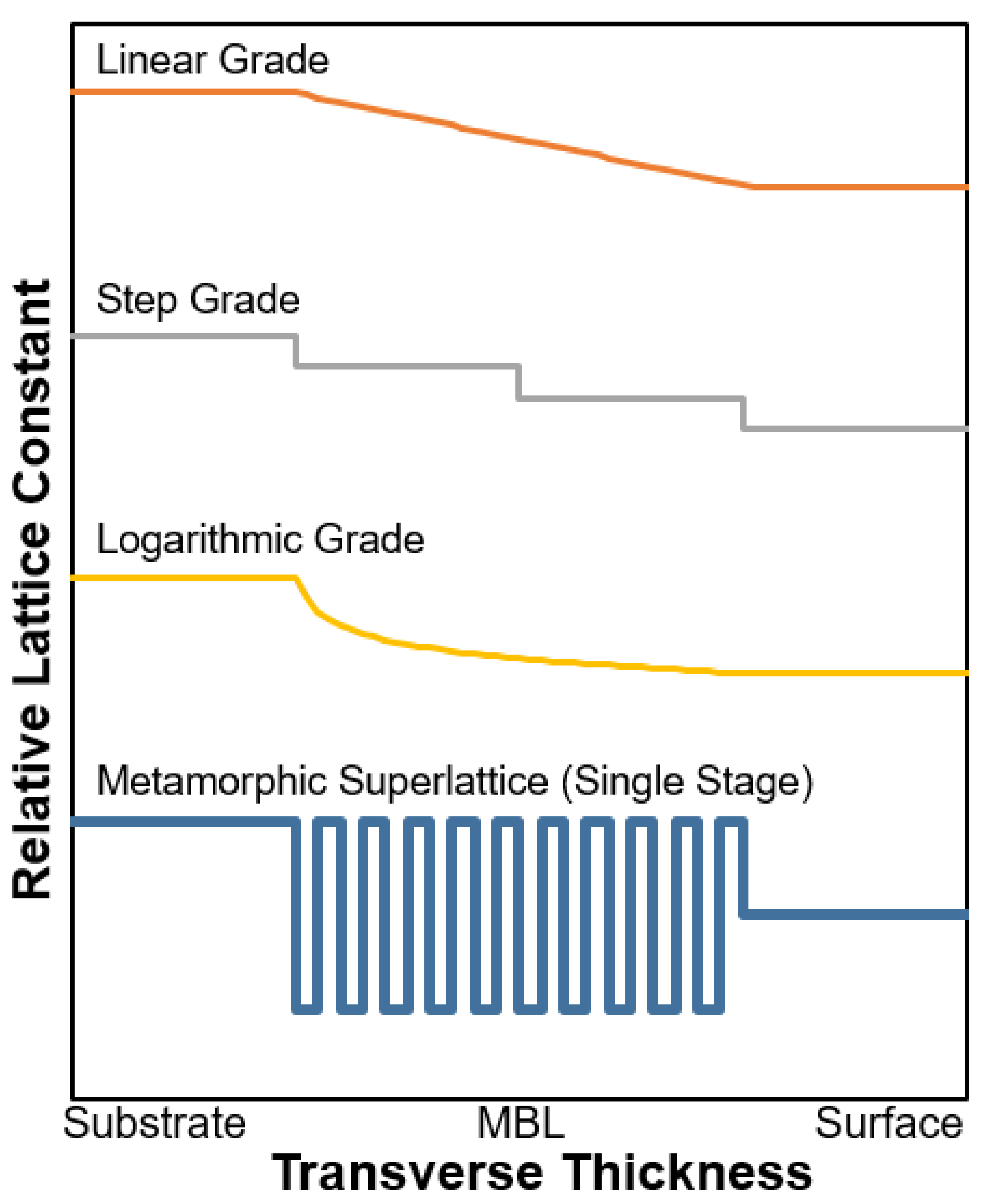
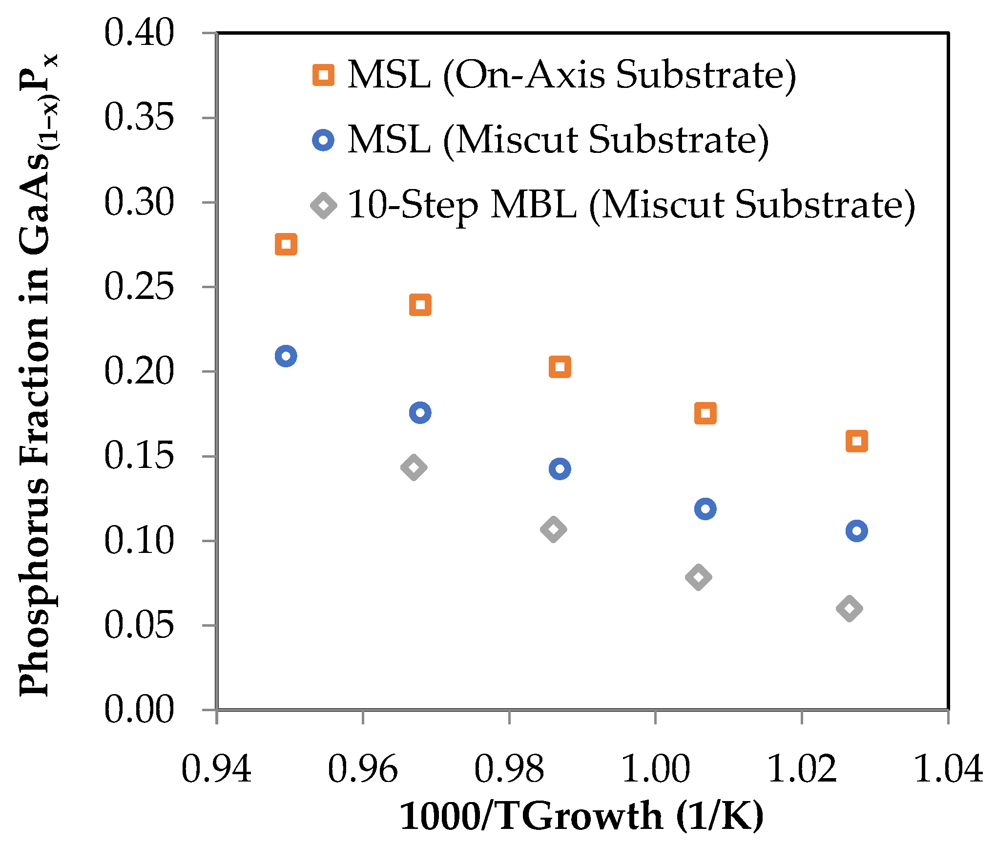
2.2. Metamorphic GaAsP

MBL and MSL structures were grown on on-axis and 10° miscut GaAs substrates. A linearly graded MBL and an evenly distributed 10-step graded MBL with comparable nominal phosphorus fractions were grown as a baseline for MBL material quality characterization. Multi-stage MSLs were compared over a range of 4–10 stages and at growth temperatures ranging from 680 °C to 760 °C measured by k-type thermocouple at the reactor susceptor. Photoluminescence (PL) spectroscopy was used to estimate the bandgap of the GaAsP layers. X-ray diffractometry (XRD) and reciprocal space mapping (RSM) were used to extract in-plane and out-of-plane lattice constants, tilt, and relaxation for a 4-stage MSL structure. The surface roughness of the as-grown epitaxial structures was measured by white light interferometry and atomic force microscopy (AFM). TDD was estimated using cathodoluminescence (CL).

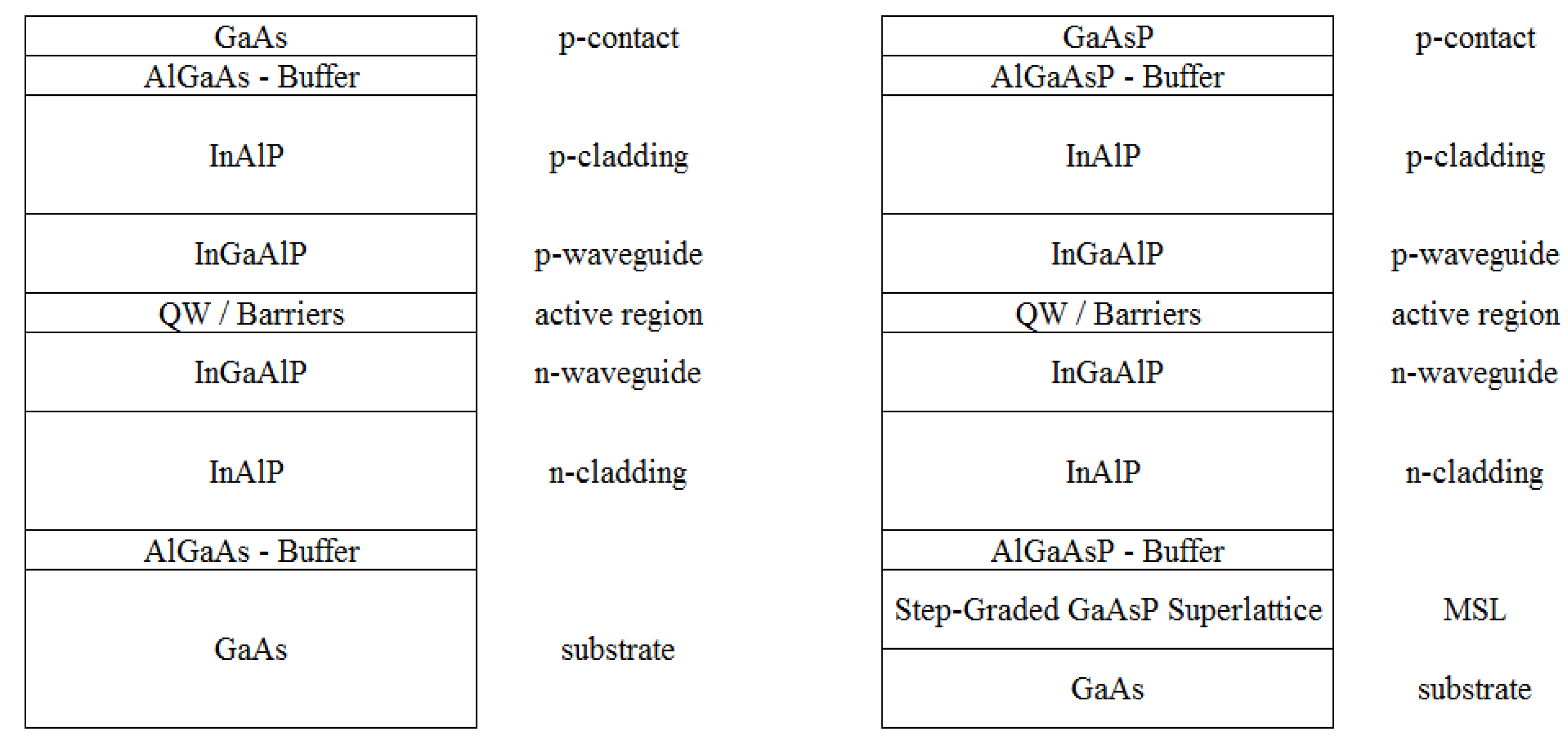
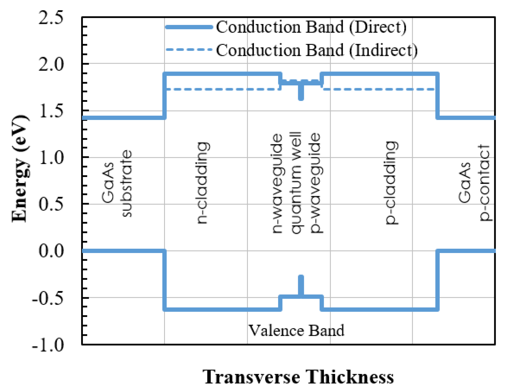
2.3. Laser Diode Structures

The baseline laser diode structure and MSL-based structure consist of GaAs(P)/InGaAlP-based materials and are shown schematically in Figure 2 and the relative band offsets for the baseline structure on GaAs are shown in Figure 3. Indices for these materials have been described in the literature [12]. In addition to the baseline structure, iterations of that structure were grown for the optimization of cladding layer thickness and chip dimension. The MSL-based laser structure used a 4-stage MSL as the virtual substrate and a modified baseline laser structure consisting of GaAsP/InGaAlP layers that were nominally lattice matched to the virtual substrate.
Cavity length analysis (CLA) was performed to extract internal properties of the device material using chips with uncoated facets and lengths ranging from 1.5 to 3.0 mm. Chips with highly reflective/anti-reflective (HR/AR) facet coatings were then mounted using AuSn on CuW and tested under continuous wave (CW) operation.

3. Results and Discussion

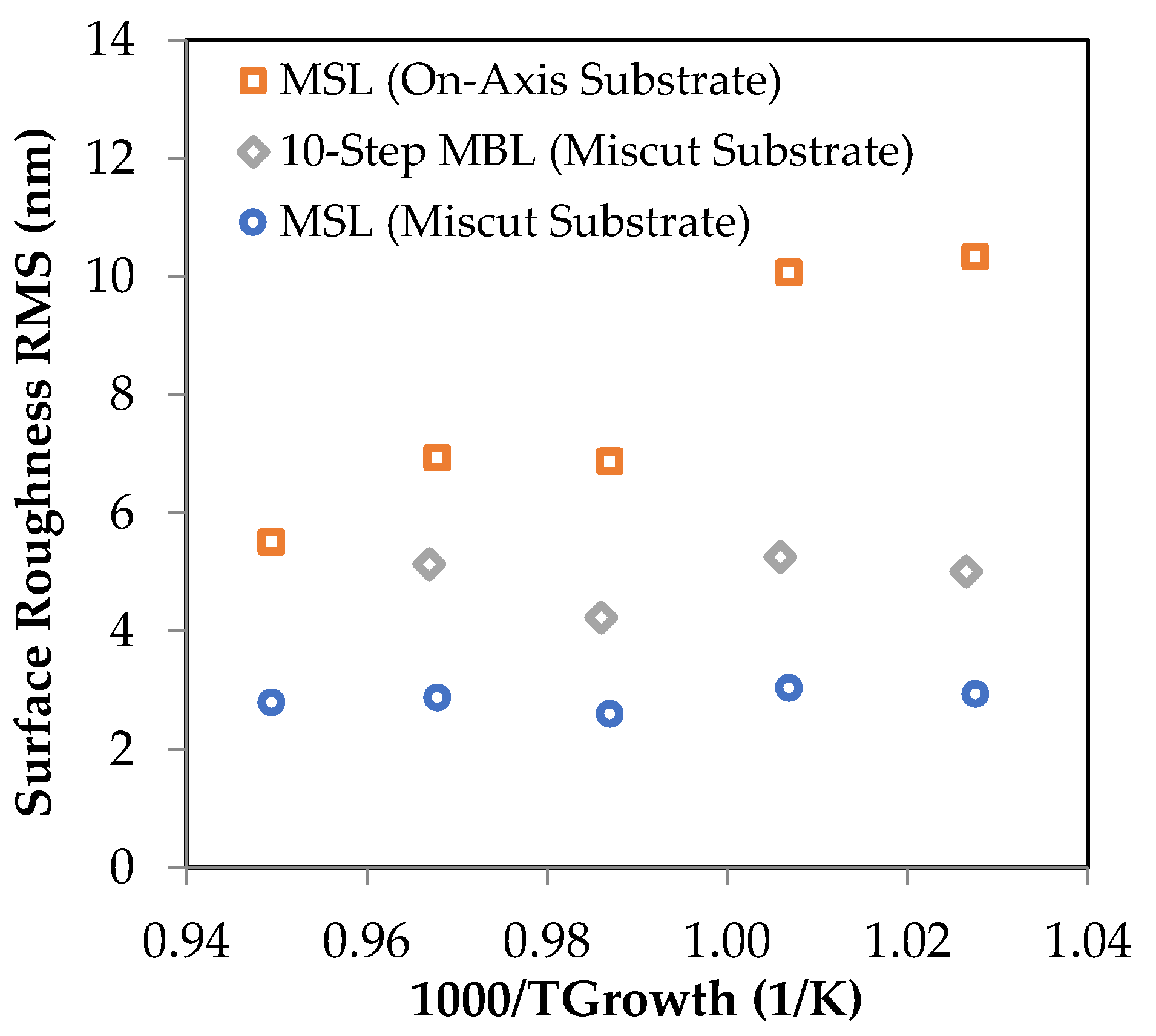
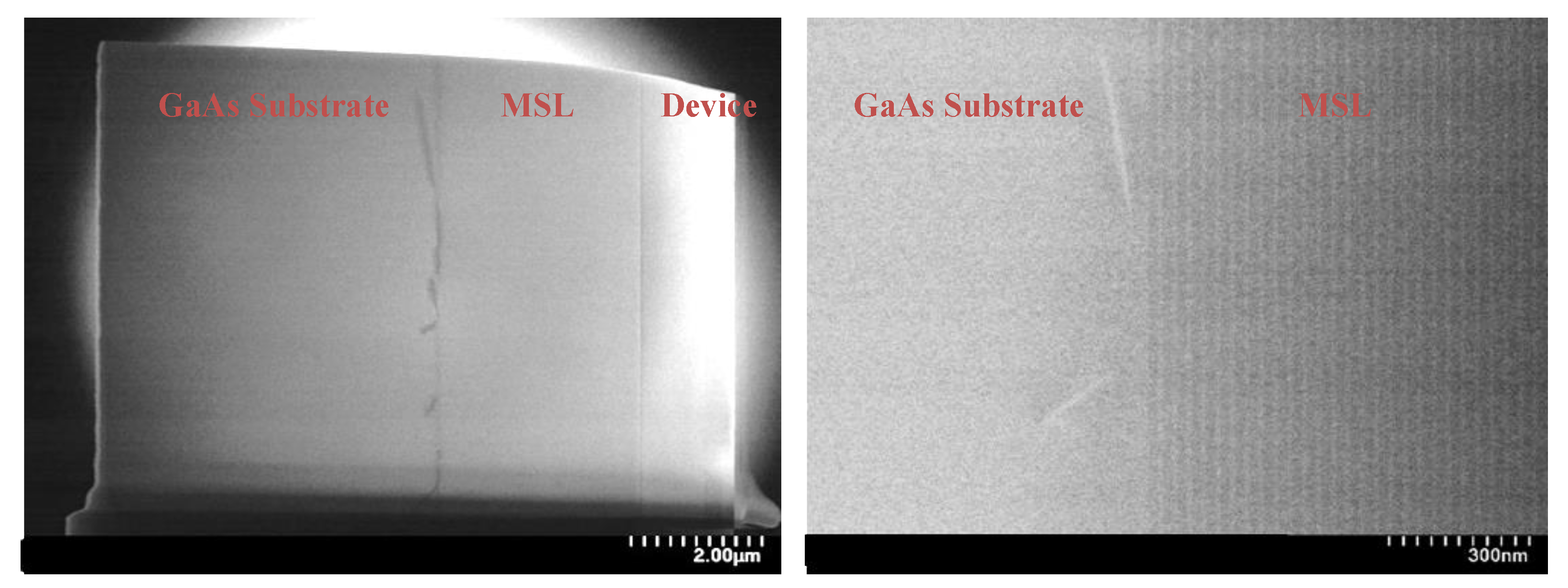
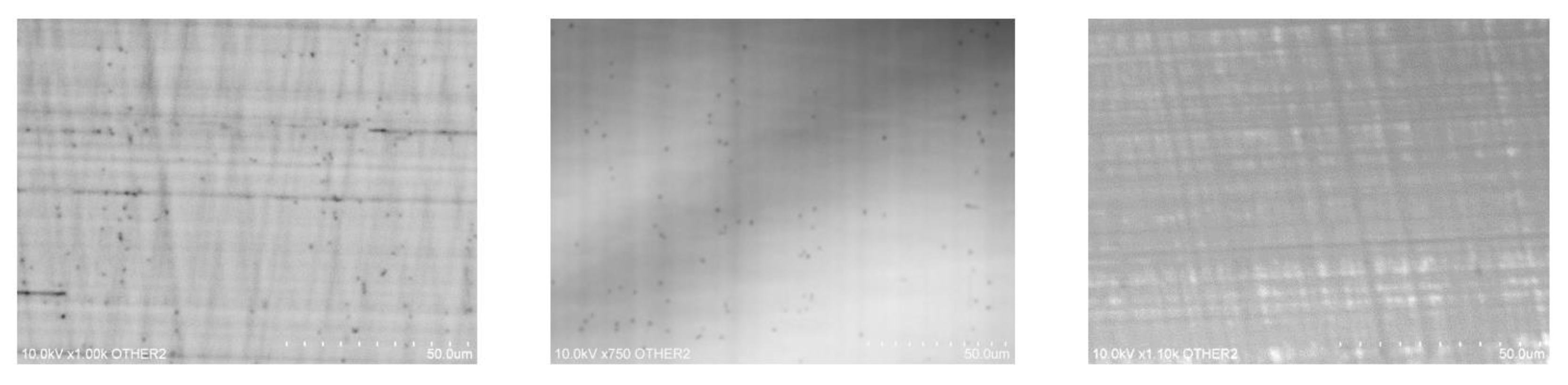
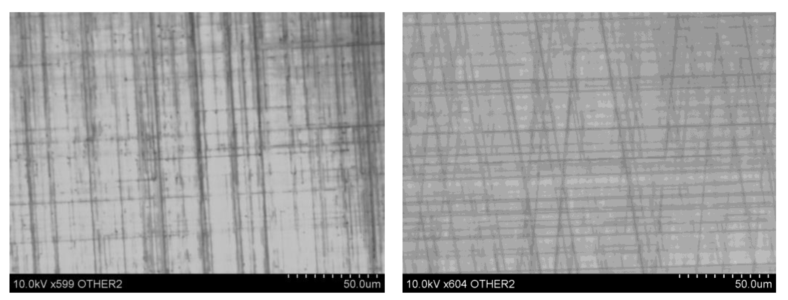
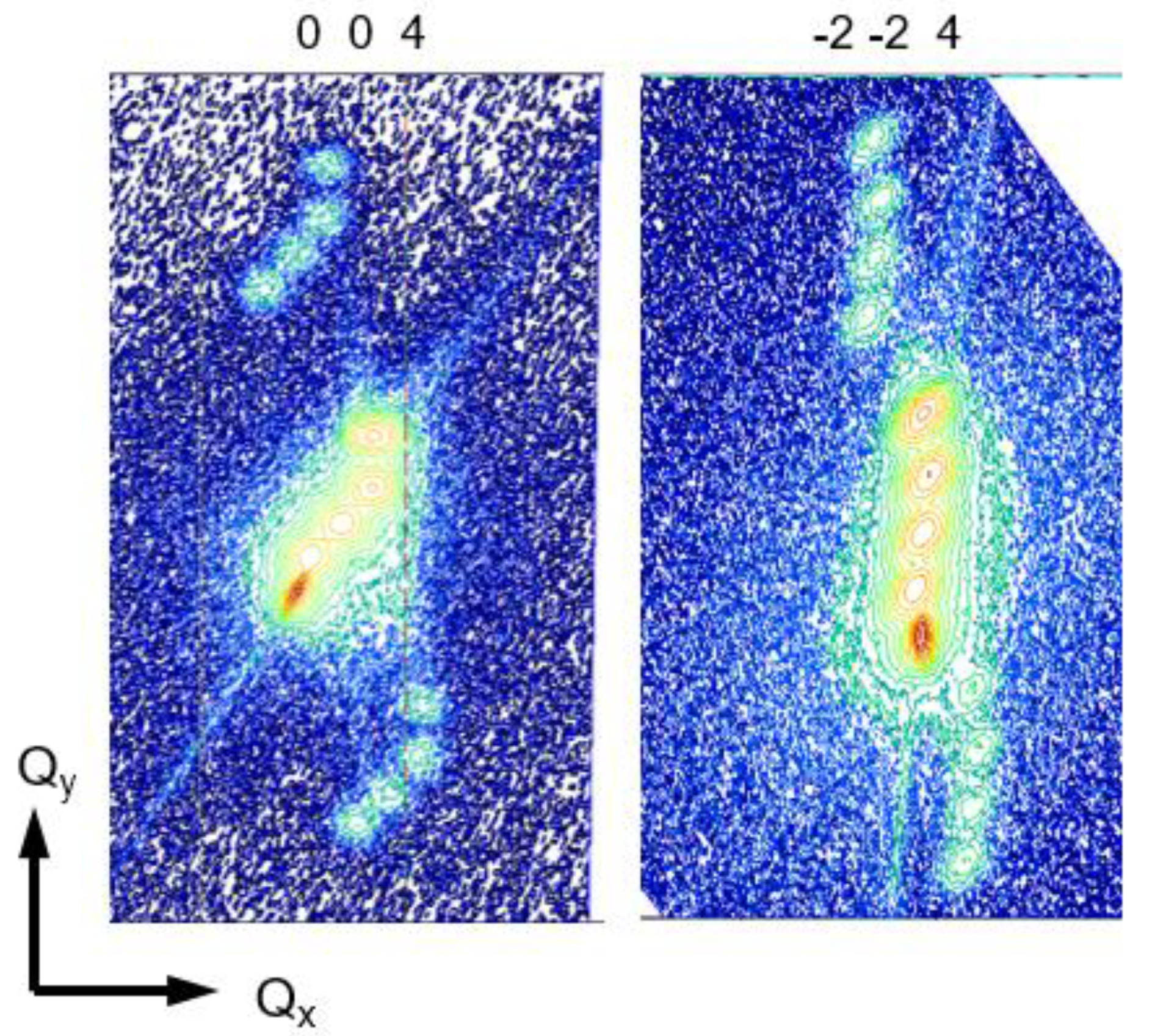
3.1. Metamorphic GaAsP

The cathodoluminescence surface scans of the linearly graded and 10-step graded MBL, as well as the 4-stage MSL, are shown in Figure 4. The graded regions were approximately 2.5 μm thick and steps or stages were distributed evenly throughout the grade. Each sample’s surface composition was approximately GaAs0.82P0.18 based on the PL emission wavelength. Threading dislocations result in non-radiative recombination and since they propagate through the growth plane, they are represented by dark spots [13]. The dark lines are thought to indicate buried misfit dislocations, which run along the {111} glide planes. Table 1 shows the TDD and surface roughness for each of these three MBLs.
In addition to MBL type, the wafer miscut angle also affects surface roughness and crosshatching orientation. The crosshatch orientation for the different substrate miscuts is visible in the cathodoluminescence images in Figure 5 in the form of misfit dislocations. The standard substrate has orthogonal misfit dislocations, while the material grown on the miscut substrate has tilted dislocations consistent with the intersection of {111} planes and the epitaxial growth plane.
Photoluminescence measurements indicate that, in addition to gas-phase PH3/V during growth, the phosphorous incorporation is also dependent on both the growth temperature and the substrate miscut. Solid-state phosphorus fractions are plotted in Figure 6 for both substrate orientations over a range of growth temperatures with consistent PH3/V flows in each growth. In addition, surface roughness is plotted for these samples in Figure 7. These data demonstrate that surface roughness decreases at elevated growth temperatures, despite also increasing phosphorus fraction and overall mismatch with the underlying substrate. The MSL appears to be able to maintain a relatively low surface roughness, even with large compositional shifts with high-temperature growth.
The in-plane and out-of-plane lattice constants for individual layers of the 4-stage MSL were extracted from the RSM data shown in Figure 8, and the parameters are summarized in Table 2. The maps reveal a high intensity substrate peak, four main peaks thought to correspond to the net material composition of each MSL stage, and eight satellite peaks corresponding to the wells and barriers of each MSL stage. Each of these layers resolve as distinct peaks, indicating that the MSL relaxes to a strain-balanced equilibrium in each stage with a common in-plane lattice constant throughout that stage. In addition to a reduction in lattice constant, the MSL layers have a measurable tilt in the direction of the substrate miscut, which is consistent with previous MBL growth studies [14,15].

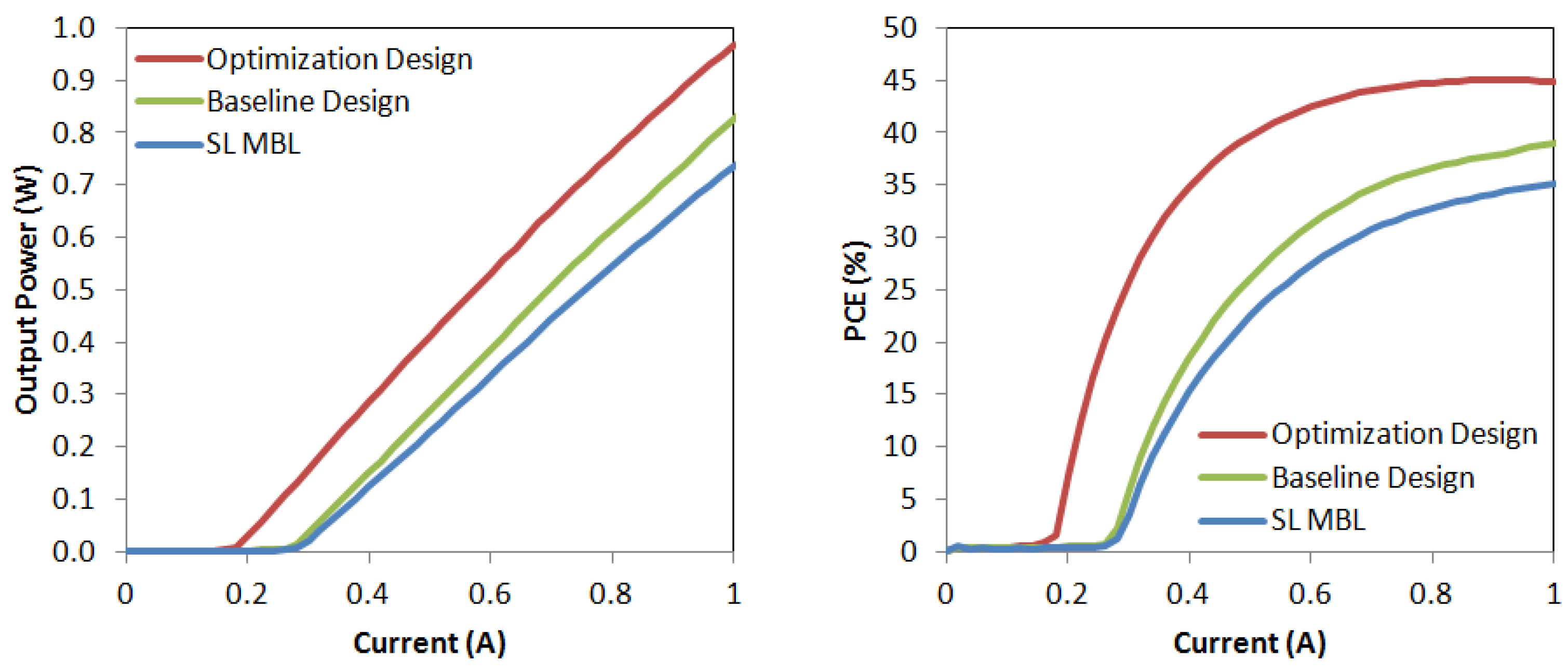
3.2. Laser Diode Structures

The MSL used in this study for the laser diode virtual substrate terminated at an approximate net composition of GaAs(1−x)Px, where x = 0.04, corresponding to a relaxed lattice constant of 5.645 Å, based on bandgap estimation from photoluminescence. Cathodoluminescence measurements of the MSL without the laser diode structure indicate a threading dislocation density of 4 × 10⁴/cm2 and a surface roughness of 1.17 nm RMS was measured by white light interferometry. TEM measurements show that the QW in the MSL-based heterostructure was 6.3 nm thick with the InxGa(1−x)P composition estimated at x = 0.487, corresponding to a compressive strain of 0.17%. TEM micrographs of the substrate and MSL interfaces indicate an accumulation of defects within the substrate near the MSL interface, while dislocations were not observed in the MSL cross section (Figure 9).
The device parameters of the three structures extracted by CLA are summarized in Table 3. The optimized baseline structure on the standard GaAs substrate incorporates a thinned p-cladding and longer emission wavelength. The thinner p-cladding reduces thermal impedance and junction temperature, while the narrower QW bandgap increases relative band offsets of the separate confinement heterostructure (SCH) and increases carrier confinement in the QW [4]. With these changes, the optimized structure shows improvements in ηi, αi, T0, and T1. In the MSL structure, there is an increase in αi, possibly attributed to additional loss from SL layer interfaces and crystal defects associated with misfit and threading dislocations from lattice strain relaxation. However, the baseline structure on the MSL exhibits the highest ηi, T0, and T1, which may lead to improved relative performance at higher operating temperatures or shorter wavelengths due to enhanced carrier confinement. QW strain in these lasers determines the emission polarization by shifting the relative energy of light hole (LH) and heavy hole (HH) bands, which leads to CS QWs to favor TE polarization from HH transitions and TS QWs to favor TM polarization from LH transitions [16]. While CS QWs can be used for short wavelengths (<640 nm) directly on GaAs substrates, the highest performance has been obtained from employing TS QWs [17]. This is largely influenced by the inability to reduce emission wavelength in CS InGaP QWs compositionally beyond the GaAs lattice-matched condition, so short wavelengths must be achieved using quantum size effects. This leads to very thin CS QWs at short wavelengths in traditional laser diodes on GaAs substrates. The MSL relaxes this constraint by allowing CS QWs with lower indium fractions, leading to the realization of high-performance, thicker QWs with TE laser emissions at shorter wavelengths.
Output power (LI) and PCE curves for 45 μm wide cavity single emitter chips of each design tested under CW operation are plotted in Figure 10. The optimization design reaches peak PCE of 45%, which is higher than some of the best commercially available red laser diodes [18]. Further optimization to facet coating reflectivity may yield additional increases to PCE. The MSL design is likely to benefit from similar optimizations, possibly to a greater extent, due to the relatively higher internal loss.

4. Conclusions

In this work, we demonstrated world class red laser diodes reaching 45% PCE using an optimized waveguide structure. In addition, high-performance TE emission laser diodes were realized using a compressively strained QW within a compositionally shifted laser structure on a MSL-based virtual substrate. The MSL reduced TDD and surface roughness, allowing for the growth of higher quality materials than typical MBLs. The MSL also appeared to maintain an advantage in material quality at smaller lattice constants than other MBLs. This may increase design space for higher bandgap materials, which has the potential to allow the fabrication of efficient devices while reducing emission wavelengths in InGaAlP-based red laser diodes more than possible with a traditional GaAs substrate.

Author Contributions

Conceptualization, S.R., T.E. and L.J.M.; methodology, S.R., T.E. and L.J.M.; validation, S.R., C.G., M.K. and D.O.; formal analysis, S.R., T.E. and L.J.M.; writing—review and editing, S.R., T.E. and L.J.M. All authors have read and agreed to the published version of the manuscript.

Funding

This research received no external funding.

Data Availability Statement

Not applicable.

Conflicts of Interest

The authors declare no conflict of interest.

References

  1. Overton, G. Mobile projection technologies proliferate. Laser Focus World 2007, 43, 67–70. [Google Scholar]
  2. Buckley, E. Holographic Laser Projection. J. Disp. Technol. 2011, 7, 135–140. [Google Scholar] [CrossRef]
  3. Angelov, I.P. Light enhancement of in vitro antitumor activity of galactosylated phthalocyanines. Photonics Lasers Med. 2016, 5, 123–140. [Google Scholar] [CrossRef]
  4. Nishida, T.; Shimada, N.; Ogawa, T.; Miyashita, M.; Yagi, T. Short Wavelength Limitation in High Power AlGaInP Laser Diodes. Proc. SPIE 2011, 2011, 791811. [Google Scholar]
  5. Saha, S.K. Different Approaches to Improve Metamorphic Buffer Layers Grown on a GaAs Substrate. Master’s Thesis, McMaster University, Hamilton, ON, Canada, 2009. [Google Scholar]
  6. Galiev, G.B.; Vasil’Evskii, I.S.; Pushkarev, S.S.; Klimov, E.A.; Imamov, R.M.; Buffat, P.A.; Dwir, B.; Suvorova, E.I. Metamorphic InAlAs/InGaAs/InAlAs/GaAs HEMT heterostructures containing strained superlattices and inverse steps in the metamorphic buffer. J. Cryst. Growth 2013, 366, 55–60. [Google Scholar] [CrossRef]
  7. Fischer, R.; Morkoc, H.; Neumann, D.A.; Zabel, H.; Choi, C.; Otsuka, N.; Longerbone, M.; Erickson, L.P. Material properties of high-quality GaAs epitaxial layers grown on Si substrates. J. Appl. Phys. 1986, 60, 1640–1647. [Google Scholar] [CrossRef]
  8. Yamaguchi, M.; Nishioka, T.; Sugo, M. Analysis of strained-layer superlattice effects on dislocation density reduction in GaAs on Si substrates. Appl. Phys. Lett. 1989, 54, 1. [Google Scholar] [CrossRef]
  9. Kim, H.; Shi, B.; Lingley, Z.; Li, Q.; Rajeev, A.; Brodie, M.; Lau, K.M.; Kuech, T.F.; Sin, Y.; Mawst, L.J. Electrically injected 1.64 µm emitting In0.65Ga0.35As 3-QW laser diodes grown on mismatched substrates by MOVPE. Opt. Express 2019, 27, 33205–33216. [Google Scholar] [CrossRef] [PubMed]
  10. Matthews, J.W. Defects associated with the accommodation of misfit between crystals. J. Vac. Sci. Technol. 1975, 12, 126–133. [Google Scholar] [CrossRef]
  11. Matthews, J.W.; Blakeslee, A.E. Defects in epitaxial multilayers. J. Cryst. Growth 1974, 27, 118–125. [Google Scholar] [CrossRef]
  12. Bour, D.P. AlGaInP Quantum Well Lasers. In Quantum Well Lasers; Zory, P.S., Ed.; Academic Press: London, UK, 1993; pp. 415–453. [Google Scholar]
  13. Petroff, P.M.; Weisbuch, C.; Dingle, R.; Gossard, A.C.; Wiegmann, W. Luminescence properties of GaAs-Ga(1-x)Al(x)As double heterostructures and multiquantum-well superlattices grown by molecular beam epitaxy. Appl. Phys. Lett. 1981, 38, 965–967. [Google Scholar] [CrossRef]
  14. Lee, D.; Park, M.S.; Tang, Z.; Luo, H.; Beresford, R.; Wie, C.R. Characterization of metamorphic InxAl1−xAs/GaAs buffer layers using reciprocal space mapping. J. Appl. Phys. 2007, 101, 063523-1-8. [Google Scholar] [CrossRef] [Green Version]
  15. Schulte, K.L.; Strand, M.T.; Kuech, T.F. Evolution of epilayer tilt in thick In(x)Ga(1-x)As metamorphic buffer layers grown by hydride vapor phase epitaxy. J. Cryst. Growth 2015, 426, 283–286. [Google Scholar] [CrossRef] [Green Version]
  16. Bour, D.P.; Geels, R.S.; Treat, D.W.; Paoli, T.L.; Ponce, F.; Thornton, R.L.; Krusor, B.S.; Bringans, R.D.; Welch, D.F. Strained GaxIn1-xP/(AlGa)0.5In0.5P Heterostructures and Quantum-Well Laser Diodes. J. Quantum Electron. 1994, 30, 593–607. [Google Scholar] [CrossRef]
  17. Yagi, T.; Kuramoto, K.; Kadoiwa, K.; Wakamatsu, R.; Miyashita, M. Reliability study on high power 638-nm triple emitter broad area laser diode. Proc. SPIE 2016, 9733, 973305. [Google Scholar]
  18. Nishida, T.; Kuramoto, K.; Iwai, Y.; Fujita, T.; Yagi, T. Multiemitter 638-nm high-power broad area laser diodes for display application. Opt. Eng. 2019, 58, 086113. [Google Scholar] [CrossRef]
Figure 1. Schematic comparing metamorphic buffer layer composition profiles for common buffer and a single stage MSL.
Photonics 09 00436 g001
Figure 2. Epitaxial layer structures of red laser diodes on GaAs (left) and on GaAsP MSL virtual substrate (right).
Photonics 09 00436 g002
Figure 3. Relative band offset schematic for a general red laser diode structure.
Photonics 09 00436 g003
Figure 4. Cathodoluminescence scans of linearly graded MBL (left), step-graded MBL (center), and 4-stage MSL (right) on 10° miscut substrates.
Photonics 09 00436 g004
Figure 5. Cathodoluminescence scans of a 10-stage MSL grown on on-axis substrate (left) and 10° miscut substrate (right).
Photonics 09 00436 g005
Figure 6. As-grown phosphorus fraction of terminal MBL material for various growth temperatures on on-axis and miscut substrates for 10-step MBLs and 6-stage MSLs.
Photonics 09 00436 g006
Figure 7. Surface roughness 10-step MBLs and 6-stage MSLs for various growth temperatures on on-axis and miscut substrates.
Photonics 09 00436 g007
Figure 8. X-ray diffraction 0 0 4 (left) and −2 −2 4 (right) reciprocal space maps of a four-stage metamorphic superlattice used to extract MSL layer parameters.
Photonics 09 00436 g008
Figure 9. Cross-sectional TEM micrograph of laser diode structure grown on 4-stage MSL (left) and respective substrate-MSL interface (right).
Photonics 09 00436 g009
Figure 10. LI (left) and PCE (right) curves of single-emitter red laser diodes tested under CW conditions.
Photonics 09 00436 g010
Table 1. Measured material parameters of MBLs grown by various compositional grading methods.
Linearly-Graded Step-Graded MBL MSL
MBL(10 Steps)(4 Stages)
RMS Roughness (nm)6.525.141.73
TDD (cm−2)1.1 × 1063.0 × 1057.1 × 104
Table 2. MSL layer parameters extracted from reciprocal space maps measured with high resolution.
BarrierWell
Estimated Net P
Fraction
In-Plane Lattice Const. (Å)Out-of-Plane Lattice Const. (Å)Out-of-Plane Lattice Const. (Å)Relative Tilt to <111>A
(Degrees)
Substrate0.0005.653
MSL Stage 10.0465.6445.5715.7200.048
MSL Stage 20.0855.6375.5605.7110.129
MSL Stage 30.1365.6265.5505.7010.219
MSL Stage 40.1765.6205.5385.6870.231
Table 3. Device parameters measured by cavity length analysis and CW performance.
Laser Diode DesignBaselineOptimizationBaseline on MSL
Parameter
Internal Quantum Efficiency, ηi0.9000.9180.977
Internal Loss, αi (cm⁻¹)2.381.973.96
Transparency Current Density, Jtr (A/cm2)203.1186.0173.5
Characteristic Temperature, T0 (K)617790
Characteristic Temperature, T1 (K)221266299
Polarization TMTMTE
CW Center Wavelength (nm)633.6637.8639.4
CW Peak PCE (%)39.045.035.5
Publisher’s Note: MDPI stays neutral with regard to jurisdictional claims in published maps and institutional affiliations.

