Communication

Laser Diffraction Zones and Spots from Three-Dimensional Graded Photonic Super-Crystals and Moiré Photonic Crystals

1
Department of Physics, University of North Texas, Denton, TX 76203, USA
2
Department of Electrical Engineering, University of North Texas, Denton, TX 76203, USA
*
Author to whom correspondence should be addressed.
Photonics 2022, 9(6), 395; https://doi.org/10.3390/photonics9060395
Submission received: 6 May 2022 / Revised: 26 May 2022 / Accepted: 2 June 2022 / Published: 3 June 2022
(This article belongs to the Special Issue Photonic Crystals: Physics and Devices)

Abstract

:
The laser diffraction from periodic structures typically shows isolated and sharp point patterns at zeroth and ±nth orders. Diffraction from 2D graded photonic super-crystals (GPSCs) has demonstrated over 1000 spots due to the fractional diffractions. Here, we report the holographic fabrication of three types of 3D GPSCs through nine beam interferences and their characteristic diffraction patterns. The diffraction spots due to the fractional orders are merged into large-area diffraction zones for these three types of GPSCs. Three distinguishable diffraction patterns have been observed: (a) 3 × 3 Diffraction zones for GPSCs with a weak gradient in unit super-cell, (b) 5 × 5 non-uniform diffraction zones for GPSCs with a strong modulation in long period and a strong gradient in unit super-cell, (c) more than 5 × 5 uniform diffraction zones for GPSCs with a medium gradient in unit super-cell and a medium modulation in long period. The GPSCs with a strong modulation appear as moiré photonic crystals. The diffraction zone pattern not only demonstrates a characterization method for the fabricated 3D GPSCs, but also proves their unique optical properties of the coupling of light from zones with 360° azimuthal angles and broad zenith angles.

1. Introduction

Traditional photonic crystals (PhCs) are nano/micro-structures, where the dielectric constant is periodically modulated on a length scale comparable to the operation wavelength [1]. There are many applications for two-dimensional (2D) and three-dimensional (3D) PhCs. One of the big driving forces for PhC research is its potential for integrated photonics, where laser source, single photon emitter, waveguide, filter, coupler, etc., can be integrated [2,3,4,5,6]. For applications in photovoltaic devices, PhCs can be used to enhance the photon absorption within silicon or perovskite solar cells and dye-sensitized solar cells to achieve a high power-conversion efficiency [7,8,9,10,11,12]. Moreover, PhCs can be applied to improve the light extraction efficiency of organic light emitting diode if patterned with the PhC [13,14,15,16,17].
Multiple-beam interference lithography has been used for the fabrication of two-dimensional (2D) and three-dimensional (3D) photonic crystals in large area or volume [18,19,20,21,22]. GPSCs can be fabricated by interfering two sets of beams with different cone angles [23,24,25,26,27,28]. In addition, the optical properties of these graded PhCs will be further studied as they belong to a new group of twisted photonic crystals [29,30,31,32,33], which is a subject still in its infancy.
Here, we report a holographic fabrication of 3D GPSCs through one central beam and eight side beams, where four beams are symmetrically arranged in cone geometry with a small cone angle α and four other beams with a big cone angle β. Three types of dual-period GPSCs are fabricated with a weak, medium, and strong modulation in the long period. Diffraction patterns are used for non-destructive characterization of quality and distinguishable features of the 3D GPSC.

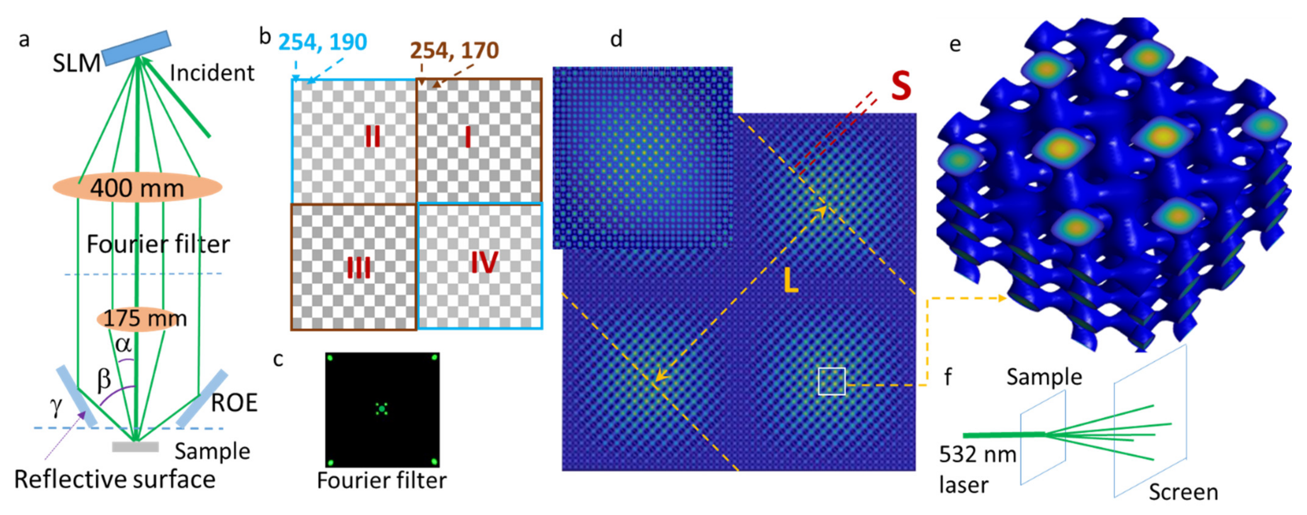
2. Experimental Methods and Theoretic Description

Figure 1a shows the experimental setup for the holographic fabrication. A 532 nm laser (total power: 50 mW, from Cobolt Samba) is incident onto a spatial light modulator (SLM) (Holoeye Pluto phase-only SLM) and linearly polarized along the long side of the SLM. The pixel size of the SLM is 8 × 8 μm2 and we assign one gray level to each pixel. These colored pixels are arranged in a unit of phase pattern as displayed in Figure 1b, which covers all 1920 × 1080 pixels on the SLM. As shown in Figure 1b, a design unit of phase patterns in the SLM is divided into four quadrants. Gray levels of 254 are combined with 190 in checkerboard format to cover a 12 × 12 pixel in quadrant II and IV. In addition, gray levels of 254 are similarly combined with 170 in checkerboard format in quadrant I and III. In Figure 1c, one central, four inner and four outer beams pass through the Fourier filter. As shown in Figure 1a, the central and four inner beams from SLM are collected by a 4f imaging system with f = 400 mm and f = 175 mm. Four outer beams are collected by the first lens and reflected by a single reflective optical element (ROE) printed by our 3D printer. The ROE has four polished silicon wafer pieces, coated with copper by thermal deposition, as the four reflective surfaces. All of the nine beams are overlapped at the sample.
The intensity of the n-beam interference, I(r), is determined by Equation (1):
I r = i = 1 n E i 2 r , t + i < j n E i E j e ^ i · e ^ j cos k j k i · r + δ j δ i  
where E, e. k, δ are the electric field amplitude, the electric field polarization direction, the wave vector, and the initial phase, respectively. For an accurate simulation of the interference pattern from multiple beams generated from the SLM, each beam needs to be assigned, pixel-by-pixel, the intensity based on the diffraction efficiency [34], and the initial phase based on the gray level [35]. Figure 1d shows a simplified interference pattern without considering the intensity and initial pixel-by-pixel phase. An enlarged view is shown in Figure 1e for woodpile-like structures, when the phase is changed from π to 0.25 π for some beams, the interference pattern shows a dot-like structure in the inset of Figure 1d rather than the woodpile-like structure.
In the simplified model, the interference pattern can have dual-periods in xy-plane, where the small and large periods are indicated by S and L in Figure 1d, respectively, and can be approximately estimated. The small period is approximately determined by the interference angle β between the central beam and outer beams in Figure 1a by Equation (2):
S = λ sin β = 0.532 sin β microns  
where S = 1.93 microns and the interference angle β = 180-2γ with the tilt angle (γ = 82 degrees) of the reflective surface in Figure 1a. The large period L is approximately determined by the 4f imaging system in Figure 1a and the unit cell size in Figure 1b. The diffraction angle θ in Figure 1a for the inner beams is determined by the unit cell size in x-direction, which is 24 pixels in Figure 1b by Equation (3):
24 pixels × sin (θ) = λ
The interference angle α between the central beam and inner beams is calculated by Equation (4):
tan α = f 1 tan θ × 2 f 2  
Considering tan(θ) ≃ sin(θ) for a small angle and length of 24 pixels = 24 × 8 = 192 microns, f = 400 mm and f = 175 mm, the large period L in the formed interference pattern in Figure 1d can be approximately calculated by Equation (5):
L = λ sin α = 192   2   175 400 = 59.4   microns  
Three types of holographic structures were fabricated in dipentaerythritol hexapentaacrylate (DPHPA) mixture with a weight percentage as follows: DPHPA monomer (88.88%), a photo initiator rose bengal (0.12%), co-initiator N-phenyl glycine (NPG, 0.8%), N-vinyl pyrrolidinone (NVP, 10.2%). The modified DPHPA mixture was typically spin-coated on glass slides at 2000 RPM for 30 s, and exposed to the interference pattern with a typical exposure time between 0.4 and 0.8 s. The exposed samples were developed in propylene glycol monomethyl ether acetate for 15 min and then allowed to air dry. The diffraction pattern was measured for three types of samples with a setup, as shown in Figure 1f.

3. Results

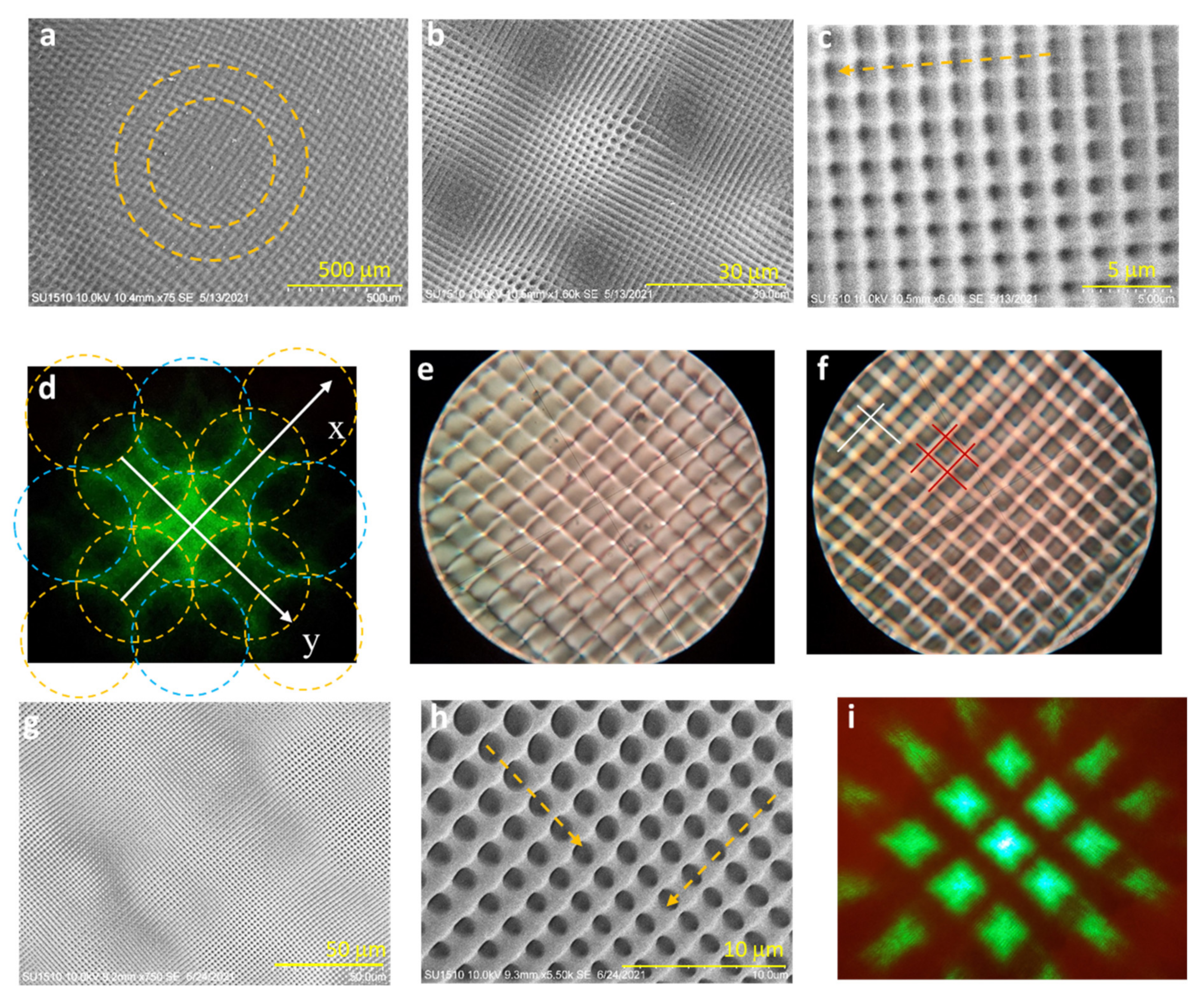
3.1. Diffraction Zone Pattern from Holographic Structures Fabricated with Type-1 Phase Pattern ((254, 190), (254, 170))

Initially, we used the type-1 phase pattern ((254, 190), (254, 170)) in Figure 1b for the imaging system alignment. Here, we present the diffraction pattern from an over-exposed sample, then from a well-developed GPSC. The over-exposed sample has a unique diffraction pattern that can be used to characterize 3D GPSCs. Figure 2a shows a scanning electron microscope (SEM) of an over-exposed type-1 3D GPSC generated using the type-1 phase pattern ((254, 190), (254, 170)) in Figure 1b. There is a weak Fresnel pattern as indicated by the dashed circles in the sample in Figure 2 due to the use of Fourier filter in Figure 1c. The weak Fresnel pattern is often used for the alignment of ROE in Figure 1a. Figure 2b,c is the enlarged view of SEM image for the sample in (a), which allow for a clear to see sample that is over-exposed. Along the dashed yellow line in Figure 2c, the air filling fraction becomes smaller, which shows the graded nature of the PhCs. The diffraction pattern from the over-exposed sample is shown in Figure 2d with a 0th order diffraction zone rather than the diffraction spot and four weak 1st order diffraction zones. These yellow and blue circles in the figure are for eye-guidance and are located following the 4-fold symmetry of GPSC and the Fresnel pattern in the sample. The edge of these diffraction zones can be fitted by these dashed yellow and blue circles periodically in [±1, ±1], [±1, 0], and [0, ±1] directions. The number of diffraction zones are determined by the long-range order of the modulated GPSC, and the diffraction spots within the diffraction zone are due to the gradient structure in the unit super-cell.
Figure 2e,f shows the Talbot diffraction pattern [36] from the over-exposed type-1 sample as observed by the optical microscope with the objective lens close to and farther away from the sample, respectively. These patterns and orientations can be understood from the 0th order and four 1st order diffractions in [±1, ±1] directions. In the top half side of Figure 2f, the Talbot diffraction pattern appears as a woodpile structure with solid red lines for the first and orthogonal second layer patterns and white lines for the third and fourth layer patterns. Below the woodpile structure, a vague Fresnel pattern appears. These Talbot patterns demonstrate all of the periodic features in the over-exposed sample.
Figure 2g shows the SEM image of a well-developed GPSC using the type-1 phase pattern ((254, 190), (254, 170)). These images show that the fabricated GPSC is in a similar structure, except for a variation in height due to the liquid DPHPA mixture. Figure 2h shows an enlarged view of the SEM image showing that the air hole size becomes smaller along both dashed yellow lines, indicating the gradient structures in the sample. The diffraction pattern in Figure 2i from the sample shows 3 × 3 diffraction zones and the 0th order diffraction spot. These diffraction zones appear in 3D GPSC, while the 2D GPSC shows fractional diffraction spots [37]. When the modulation in the long period of dual-period lattices is weak due to a slight gray level difference between (254, 190) and (254, 170), the number of uniform unit super-cell is also low. Therefore, the number of diffraction zones is also low.

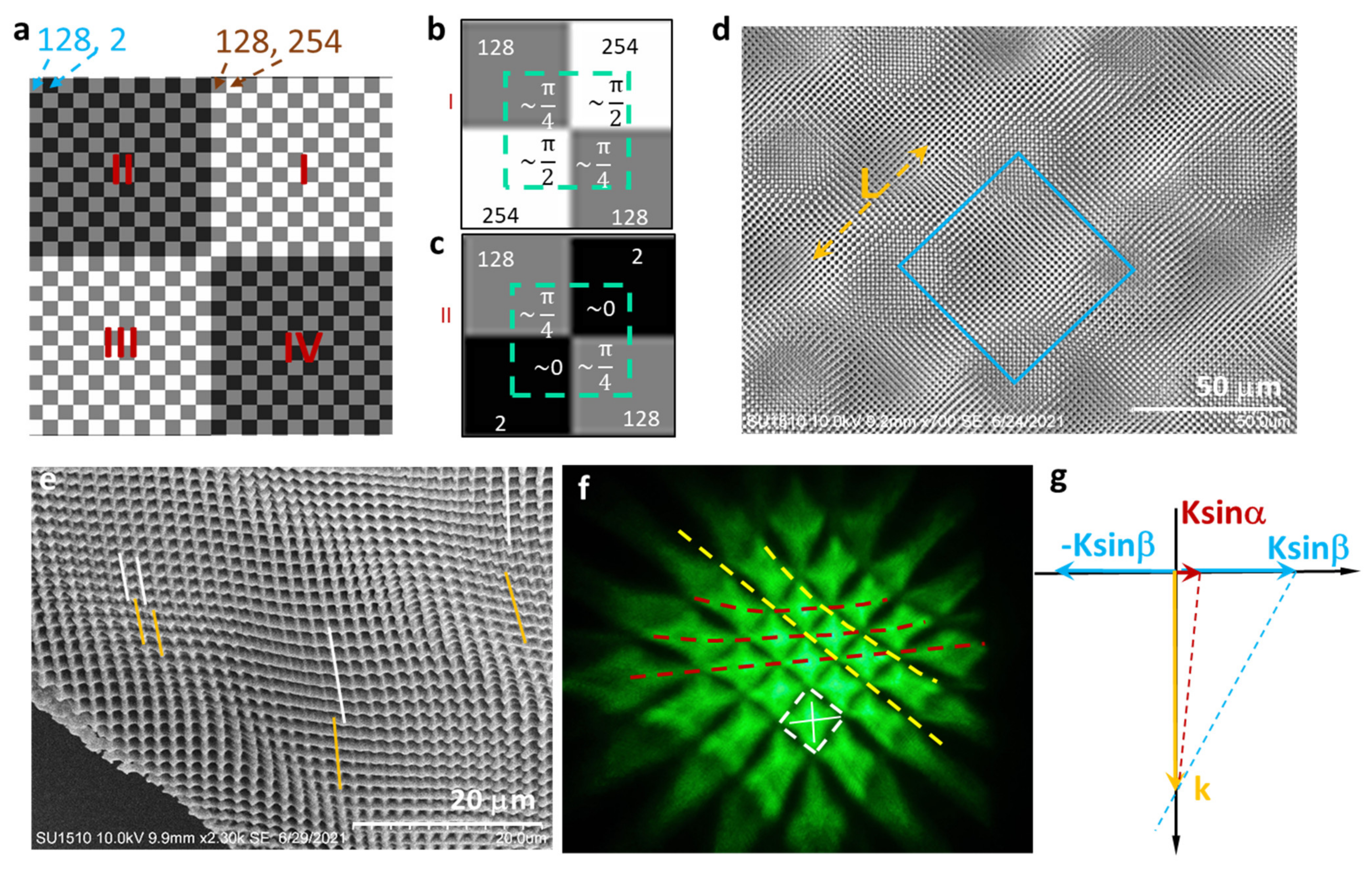
3.2. Diffraction Zone Pattern from Holographic Structures Fabricated with Type-2 Phase Pattern ((128, 2), (128, 254))

The gray levels of (128, 2) and (128, 254) are selected for the type-2 phase pattern due to their high diffraction efficiency from the checkerboard phase pattern in SLM [25,34]. The gray levels of (128, 254) cover quadrant I in Figure 3a in the checkerboard format, as shown in Figure 3b, while (128, 254) cover quadrant II in Figure 3a in the checkerboard format in Figure 3c. These phase patterns modulate the phase of outer diffracted beams through pixel-by-pixel gray levels inside the green dashed square in Figure 3b,c using the following equation: Phase = 0.25 ∗ gray level ∗ 2 π/255 [35]. The gray levels of 254, 128, and 2 generate approximately a phase of π/2, π/4, 0 π, respectively, in the diffracted beams. In Figure 3b, the phase of the outer beams in [1,1] direction is π/4 higher than these in [1,−1] direction, while they are π/4 less in [1,1] than those in the [1,−1] direction in Figure 3c. These phase differences in interfering beams will result in two different patterns, which is observed in Figure 3d, where the solid blue square indicates the unit super-cell of fabricated GSPC in DPHPA. Four regions at the vertices of the solid blue square are similar to the interference pattern in the inset of Figure 1d with the phase shift of 0.25 π. The patterns in the center of the solid blue square are similar to the woodpile-like structures in Figure 1d,e. The dashed yellow arrow indicates the long period of dual-period GPSC. Moreover, this GPSC appears as moiré PhCs. The long period L (also moiré period in this case) is measured to be 58.6 microns, compared with the theoretically calculated value of 59.4 microns. Figure 3e shows the SEM image of bottom surface of the sample when it is separated from the substrate after a longer development time than the usual one. The moiré pattern is hardly seen at the bottom of the surface. The dual lattice feature can be observed [26,34], as indicated by the white and yellow lines. It will be compared with a simulation in the next section.
Figure 3f shows the diffraction pattern of the 532 nm laser from the 3D GPSC in Figure 3d. The diffraction pattern shows almost 5 × 5 non-uniform diffraction zones. The dashed white square indicates the size of one diffraction zone. It can be divided into four sub-zones corresponding to 4-fold symmetry in the unit super-cell in Figure 3d. The edges of the diffraction zone inside the white square in Figure 3f have a parabolic shape due to the tilt of unit super-cell in 3D GPSC. It can be explained by a simple model in Figure 3g. The short period and long period of 3D GPSC in xy-plane are approximately determined by β and α, respectively, in Figure 3g. By adding these four inner beams in the interference, the 3D GPSC can be considered as tilted from the vertical direction to the one indicated by the dashed red line in Figure 3g. Overall, the diffraction zone is not uniform in intensity as indicated by the dashed red lines in Figure 3f for the position of some intensity peaks. The diffraction zones are aligned in diagonal direction as indicated by the dashed yellow (straight or parabolic) lines due to tilting.

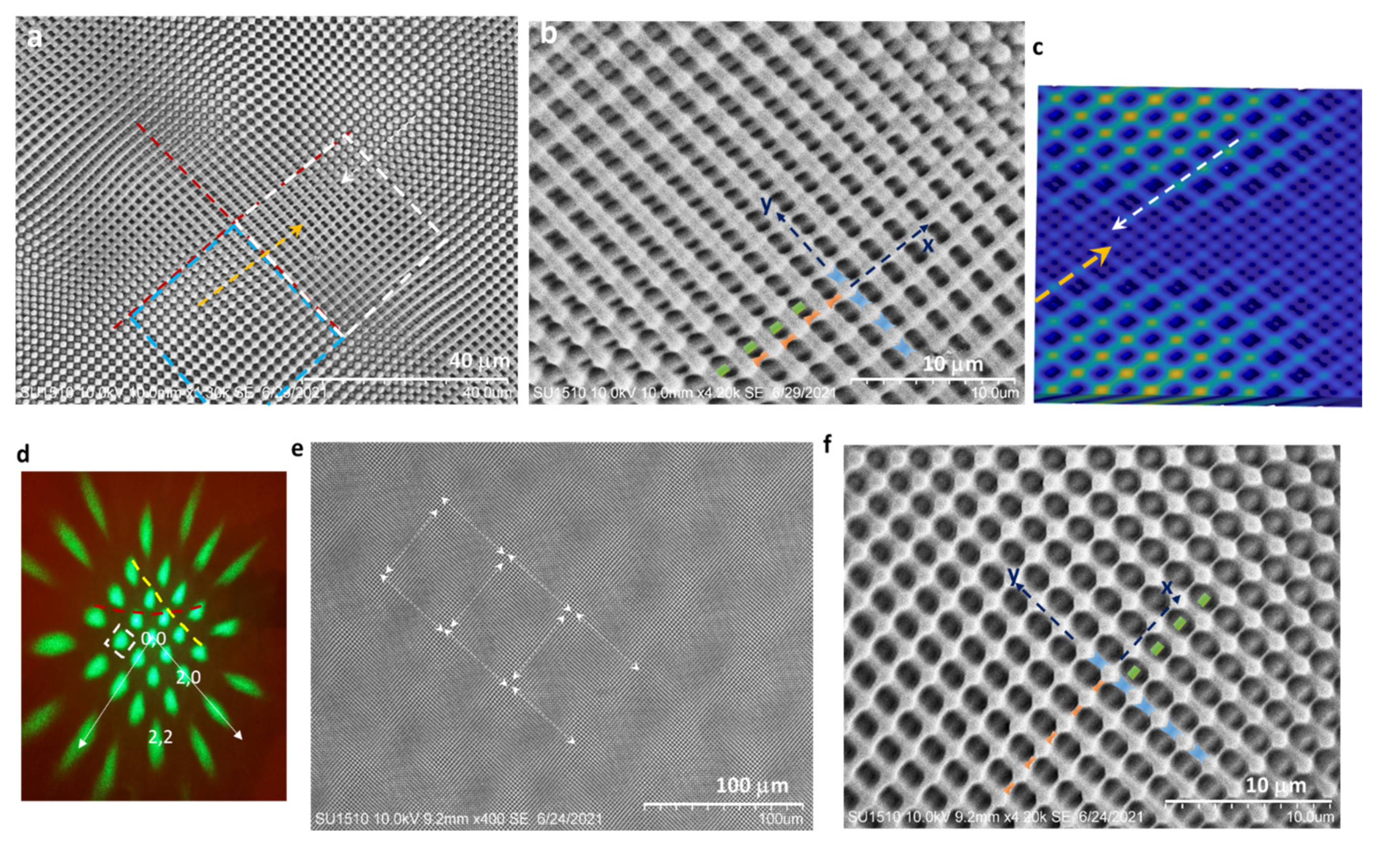
3.3. Diffraction Zone Pattern from Holographic Structures Fabricated with Type-3 Phase Pattern ((128, 2), (254, 128))

The type-3 phase pattern in the SLM is modified from type-2 in Figure 3a. The checkerboard of (128, 254) in quadrants I and III remain the same. The gray levels in the checkerboard quadrants II and IV are switched from (128, 2) to (2, 128). In this way of arrangement of gray levels, the phase of diffracted beam in Figure 3b,c is changed from (0.25, 0.5, 0.25, 0.5 π) and (0.25, 0, 0.25, 0 π) to (0.25, 0.5, 0.25, 0.5 π) and (0, 0.25, 0, 0.25 π) (clockwise from top-left) for type-3 phase pattern. This indicates that the relative phase shift for diffracted beams from top-left to top-right (also bottom-left to bottom-right) is the same for the type-3 phase pattern. Although the overall gray levels among quadrants (I, III) and (II, IV) are different for the generation of inner beams, the modulation of the unit super-cell in type-3 3D GPSC is expected to be weaker than in type-2 3D GPSC.
Figure 4a,b shows the SEM image of fabricated 3D GPSC in DPHPA using the type-3 phase pattern and its enlarged view. Due to the weak modulation, the assignment of a unit super-cell in Figure 4a is not as simple as in Figure 3d. The region inside the dashed white square in Figure 4a appears as an array of rods over an array of rods rotated by 90°, while the region inside the dashed blue square appears as dots for the joints of rods in two layers. The dual lattice feature is clearly observed in Figure 4a: The size of dots becomes smaller along the dashed yellow arrow and the dashed white arrow that is in the opposite direction to the yellow one. In addition, the yellow and white arrows are shifted by half of the small period. The experimental observation agrees with the simulation in Figure 4c with a dual lattice structure that has been observed in 2D GPSC [26,34].
Figure 4d shows the laser diffraction pattern of 532 nm from the type-3 3D GPSC, which is similar to type-2 3D GPSC. Diffraction zones in the diffraction pattern are aligned along the parabolic dashed red and yellow lines due to the tilting caused by the four inner interfering beams. The diffraction zone inside the dashed white square has a low filling fraction, but more uniform intensity due to a lower gradient in the unit super-cell than in type-2 3D GPSC.
Diffraction efficiency is measured in Table 1 for diffraction zone orders of (0, 0), (1, 0), (2, 0), (1, 1), (2, 1), and (2, 2) in Figure 4d. The diffraction zone orders of (0, 0), (2, 0), and (2, 2) are labeled in the figure. From these efficiency numbers, we can see that most of the light are distributed among non-zero orders. For example, 24% of light is distributed in (±1, 0) and (0, ±1) orders, compared with 9.9% for (0, 0) order.

4. Discussion

The metal deposition on the SEM image sample typically destroys the sample for other purposes. Therefore, we have been using these features in the diffraction zone to quickly distinguish the different types of 3D GPSCs. These features have been consistently observed, for example, in Figure 4e from a sample that is fabricated on a different day for type-3 3D GPSC. The white arrows indicate the repeatability of patterns with a higher filling fraction of air in DPHPA GPSC than the other regions. Layer-by-layer structures are visible in Figure 4b,f where the dashed orange lines in x-axis indicate the top layer, dashed blue lines in y-axis indicate the second layer, and dashed green lines indicate the third layer that is shifted by half of the lattice period.
DPHPA mixture is a good polymer for a quick proof of concept of holographic structures. However, it is in a liquid form, has a thin film, and is polymerized during the exposure, which makes it suboptimal for 3D structures. SU-8 should be used for 3D structure in future work as it is in a solid form and polymerized during post-exposure heating [21,38,39]. In addition, it is a good template for an inversion to silicon materials [40]. With a thick sample in SU-8, it will be interesting to observe the diffraction pattern from a different direction as one research group did for super-crystals with complex macroscopic properties in composite ferroelectrics [41].
The study of 3D GPSC is still in its infancy. It can lead toward many potential applications due to the tunability of holographic patterns by phase, intensity, and polarization of interfering beams. The 3D holographic structures have been studied for their topological properties [22]. Once the interference pattern is inversed to a silicon structure (dielectric constant = 11.9) using the following step functions: ε(r) = 1 when I < Ith; ε(r) = 11.9 when I > Ith [38], we can conduct simulations of photonic band structure to search for multiple photonic band-gaps and flat bands or electro-magnetic simulation for diffraction patterns and focusing properties [37]. For light coupling into 3D GPSC, the type-2 GPSC can couple light from 360° azimuthal angles and broad zenith angles with less angle gap than type-3 GPSC, while type-3 GPSC can couple light more uniformly than type-2 GPSC.
To date, we have used four inner beams at (±1, ±1) for the nine-beam interference. Further study can include the other four beams at (±1, 0) and (0, ±1) in the nine-beam interference. In this case, the long period structure will be rotated by 45°.

5. Conclusions

In this paper, we have fabricated 3D GPSCs in DPHPA from nine-beam (four inner, four outer beams and one central beam arranged in a cone geometry) interference lithography using the integrated system of SLM, 4f imaging system, and single ROE. In addition, we have designed three-types of 3D GPSCs through the engineering of phase pattern in SLM by considering the diffraction efficiency, relative phase shift among the diffracted beams, and modulation of phase pattern for the generation of gradient unit super-cell. As a result, we have observed diffraction zones rather than diffraction spots due to the fractional diffraction from the unit super-cell. Moreover, we have observed 3 × 3 diffraction zones from 3D GPSCs with a weak modulation from inner beams, 5 × 5 non-uniform diffraction zones with a strong gradient unit super-cell, and 5 × 5 uniform diffraction zones with a medium gradient unit super-cell. Furthermore, moiré PhCs appear in the holographic structure with a strong modulation. Based on our observations, these diffraction patterns have been used to characterize 3D GPSCs.

Author Contributions

Conceptualization, Y.L. and J.C.; methodology, Y.L., N.H., S.K., K.A. and J.C.; software, N.H., K.A. and S.K.; investigation, U.P., Y.L., N.H. and S.K.; formal analysis, Y.L. and N.H.; writing—original draft preparation, N.H. and Y.L.; writing—review and editing, N.H.; funding acquisition, J.C. and Y.L. All authors have read and agreed to the published version of the manuscript.

Funding

This research was partially supported by the US National Science Foundation, grant numbers 1661842 and 2128367.

Institutional Review Board Statement

Not applicable.

Informed Consent Statement

Not applicable.

Data Availability Statement

Data will be available upon request.

Conflicts of Interest

The authors declare no conflict of interest. The funders had no role in the design of the study; in the collection, analyses, or interpretation of data; in the writing of the manuscript, or in the decision to publish the results.

References

  1. John, S. Strong Localization of Photons in Certain Disordered Dielectric Superlattices. Phys. Rev. Lett. 1987, 58, 2486–2489. [Google Scholar] [CrossRef] [PubMed] [Green Version]
  2. Akahane, Y.; Asano, T.; Song, B.S.; Noda, S. High-Q Photonic Nanocavity in a Two-Dimensional Photonic Crystal. Nature 2003, 425, 944–947. [Google Scholar] [CrossRef] [PubMed]
  3. Tandaechanurat, A.; Ishida, S.; Guimard, D.; Nomura, M.; Iwamoto, S.; Arakawa, Y. Lasing Oscillation in a Three-Dimensional Photonic Crystal Nanocavity with a Complete Bandgap. Nat. Photonics 2011, 5, 91–94. [Google Scholar] [CrossRef] [Green Version]
  4. Delgoffe, A.; Miranda, A.; Rigal, B.; Lyasota, A.; Rudra, A.; Dwir, B.; Kapon, E. Tilted-Potential Photonic Crystal Cavities for Integrated Quantum Photonics. Opt. Express 2019, 27, 21822–21833. [Google Scholar] [CrossRef]
  5. Perczel, J.; Borregaard, J.; Chang, D.E.; Yelin, S.F.; Lukin, M.D. Topological Quantum Optics Using Atomlike Emitter Arrays Coupled to Photonic Crystals. Phys. Rev. Lett. 2020, 124, 83603–83610. [Google Scholar] [CrossRef] [Green Version]
  6. Kim, S.; Fröch, J.E.; Christian, J.; Straw, M.; Bishop, J.; Totonjian, D.; Watanabe, K.; Taniguchi, T.; Toth, M.; Aharonovich, I. Photonic Crystal Cavities from Hexagonal Boron Nitride. Nat. Commun. 2018, 9, 2623. [Google Scholar] [CrossRef]
  7. Bhattacharya, S.; Baydoun, I.; Lin, M.; John, S. Towards 30% Power Conversion Efficiency in Thin-Silicon Photonic-Crystal Solar Cells. Phys. Rev. Appl. 2019, 11, 14005–14031. [Google Scholar] [CrossRef] [Green Version]
  8. Liu, W.; Ma, H.; Walsh, A. Advance in Photonic Crystal Solar Cells. Renew. Sustain. Energy Rev. 2019, 116, 109436. [Google Scholar] [CrossRef]
  9. Hassan, S.; Alnasser, K.; Lowell, D.; Lin, Y. Effects of Photonic Band Structure and Unit Super-Cell Size in Graded Photonic Super-Crystal on Broadband Light Absorption in Silicon. Photonics 2019, 6, 50. [Google Scholar] [CrossRef] [Green Version]
  10. Maho, A.; Lobet, M.; Daem, N.; Piron, P.; Spronck, G.; Loicq, J.; Cloots, R.; Colson, P.; Henrist, C.; Dewalque, J. Photonic Structuration of Hybrid Inverse-Opal TiO2- Perovskite Layers for Enhanced Light Absorption in Solar Cells. ACS Appl. Energy Mater. 2021, 4, 1108–1119. [Google Scholar] [CrossRef]
  11. Lobet, M.; Piron, P.; Dewalque, J.; Maho, A.; Deparis, O.; Henrist, C.; Loicq, J. Efficiency Enhancement of Perovskite Solar Cells Based on Opal-like Photonic Crystals. Opt. Express 2019, 27, 32308–32322. [Google Scholar] [CrossRef]
  12. Hwang, D.K.; Lee, B.; Kim, D.H. Efficiency Enhancement in Solid Dye-Sensitized Solar Cell by Three-Dimensional Photonic Crystal. RSC Adv. 2013, 3, 3017–3023. [Google Scholar] [CrossRef]
  13. Kim, Y.D.; Han, K.-H.; Park, S.-J.; Kim, J.-B.; Shin, J.-H.; Kim, J.J.; Lee, H. Enhanced Light Extraction Efficiency in Organic Light Emitting Diodes Using a Tetragonal Photonic Crystal with Hydrogen Silsesquioxane. Opt. Lett. 2014, 39, 5901–5904. [Google Scholar] [CrossRef]
  14. Ishihara, K.; Fujita, M.; Matsubara, I.; Asano, T.; Noda, S.; Ohata, H.; Hirasawa, A.; Nakada, H.; Shimoji, N. Organic Light-Emitting Diodes with Photonic Crystals on Glass Substrate Fabricated by Nanoimprint Lithography. Appl. Phys. Lett. 2007, 90, 111114. [Google Scholar] [CrossRef]
  15. Zhang, Y.; Biswas, R. High Light Outcoupling Efficiency from Periodically Corrugated OLEDs. ACS Omega 2021, 6, 9291–9301. [Google Scholar] [CrossRef]
  16. Hassan, S.; Lowell, D.; Lin, Y. High Light Extraction Efficiency into Glass Substrate in Organic Light-Emitting Diodes by Patterning the Cathode in Graded Superlattice with Dual Periodicity and Dual Basis. J. Appl. Phys. 2017, 121, 233104. [Google Scholar] [CrossRef]
  17. Alnasser, K.; Hassan, S.; Kamau, S.; Zhang, H.; Lin, Y. Enhanced Light Extraction from Organic Light-Emitting Diodes by Reducing Plasmonic Loss through Graded Photonic Super-Crystals. J. Opt. Soc. Am. B 2020, 37, 1283–1289. [Google Scholar] [CrossRef]
  18. Ning, H.; Pikul, J.H.; Zhang, R.; Li, X.; Xu, S.; Wang, J.; Rogers, J.A.; King, W.P.; Braun, P.V. Holographic Patterning of High-Performance on-Chip 3D Lithium-Ion Microbatteries. Proc. Natl. Acad. Sci. USA 2015, 112, 6573–6578. [Google Scholar] [CrossRef] [Green Version]
  19. Kamali, S.M.; Arbabi, E.; Kwon, H.; Faraon, A. Metasurface-Generated Complex 3-Dimensional Optical Fields for Interference Lithography. Proc. Natl. Acad. Sci. USA 2019, 116, 21379–21384. [Google Scholar] [CrossRef] [Green Version]
  20. Jeon, T.; Kim, D.H.; Park, S.G. Holographic Fabrication of 3D Nanostructures. Adv. Mater. Interfaces 2018, 5, 1800330. [Google Scholar] [CrossRef]
  21. Lin, Y.; Herman, P.R.; Darmawikarta, K. Design and Holographic Fabrication of Tetragonal and Cubic Photonic Crystals with Phase Mask: Toward the Mass-Production of Three-Dimensional Photonic Crystals. Appl. Phys. Lett. 2005, 86, 071117. [Google Scholar] [CrossRef]
  22. Park, H.; Lee, S. Double Gyroids for Frequency-Isolated Weyl Points in the Visible Regime and Interference Lithographic Design. ACS Photonics 2020, 7, 1577–1585. [Google Scholar] [CrossRef]
  23. Sun, X.; Wu, F.; Wang, S.; Qi, Y.; Zeng, Y. Design of Gradient Photonic Crystal Lens Array Using Two-Parameter Hexagonal Prism Interferometer. Guangxue Xuebao/Acta Opt. Sin. 2020, 40, 0222002. [Google Scholar] [CrossRef]
  24. Behera, S.; Joseph, J. Single-Step Optical Realization of Bio-Inspired Dual-Periodic Motheye and Gradient-Index-Array Photonic Structures. Opt. Lett. 2016, 41, 3579–3582. [Google Scholar] [CrossRef]
  25. Lowell, D.; Hassan, S.; Sale, O.; Adewole, M.; Hurley, N.; Philipose, U.; Chen, B.; Lin, Y. Holographic Fabrication of Graded Photonic Super-Quasi-Crystals with Multiple-Level Gradients. Appl. Opt. 2018, 57, 6598–6604. [Google Scholar] [CrossRef]
  26. Hassan, S.; Sale, O.; Lowell, D.; Hurley, N.; Lin, Y. Holographic Fabrication and Optical Property of Graded Photonic Super-Crystals with a Rectangular Unit Super-Cell. Photonics 2018, 5, 34. [Google Scholar] [CrossRef] [Green Version]
  27. Lowell, D.; Hassan, S.; Adewole, M.; Philipose, U.; Chen, B.; Lin, Y. Holographic Fabrication of Graded Photonic Super-Crystals Using an Integrated Spatial Light Modulator and Reflective Optical Element Laser Projection System. Appl. Opt. 2017, 56, 9888–9891. [Google Scholar] [CrossRef]
  28. Sale, O.; Hassan, S.; Hurley, N.; Alnasser, K.; Philipose, U.; Zhang, H.; Lin, Y. Holographic Fabrication of Octagon Graded Photonic Supercrystal and Potential Applications in Topological Photonics. Front. Optoelectron. 2020, 13, 12–17. [Google Scholar] [CrossRef]
  29. Oudich, M.; Su, G.; Deng, Y.; Benalcazar, W.; Huang, R.; Gerard, N.J.R.K.; Lu, M.; Zhan, P.; Jing, Y. Photonic Analog of Bilayer Graphene. Phys. Rev. B 2021, 103, 214311–214321. [Google Scholar] [CrossRef]
  30. Lou, B.; Zhao, N.; Minkov, M.; Guo, C.; Orenstein, M.; Fan, S. Theory for Twisted Bilayer Photonic Crystal Slabs. Phys. Rev. Lett. 2021, 126, 136101–136107. [Google Scholar] [CrossRef]
  31. Dong, K.; Zhang, T.; Li, J.; Wang, Q.; Yang, F.; Rho, Y.; Wang, D.; Grigoropoulos, C.P.; Wu, J.; Yao, J. Flat Bands in Magic-Angle Bilayer Photonic Crystals at Small Twists. Phys. Rev. Lett. 2021, 126, 223601–223607. [Google Scholar] [CrossRef] [PubMed]
  32. Alnasser, K.; Kamau, S.; Hurley, N.; Cui, J.; Lin, Y. Photonic Band Gaps and Resonance Modes in 2d Twisted Moiré Photonic Crystal. Photonics 2021, 8, 408. [Google Scholar] [CrossRef]
  33. Alnasser, K.; Kamau, S.; Hurley, N.; Cui, J.; Lin, Y. Resonance Modes in Moiré Photonic Patterns for Twistoptics. OSA Contin. 2021, 4, 1339–1347. [Google Scholar] [CrossRef]
  34. Lowell, D.; Lutkenhaus, J.; George, D.; Philipose, U.; Chen, B.; Lin, Y. Simultaneous Direct Holographic Fabrication of Photonic Cavity and Graded Photonic Lattice with Dual Periodicity, Dual Basis, and Dual Symmetry. Opt. Express 2017, 25, 14444–14452. [Google Scholar] [CrossRef]
  35. Ohlinger, K.; Lutkenhaus, J.; Arigong, B.; Zhang, H.; Lin, Y. Spatially Addressable Design of Gradient Index Structures through Spatial Light Modulator Based Holographic Lithography. J. Appl. Phys. 2013, 114, 23102. [Google Scholar] [CrossRef]
  36. Case, W.B.; Tomandl, M.; Deachapunya, S.; Arndt, M. Realization of Optical Carpets in the Talbot and Talbot-Lau Configurations. Opt. Express 2009, 17, 20966–20974. [Google Scholar] [CrossRef]
  37. Hassan, S.; Jiang, Y.; Alnasser, K.; Hurley, N.; Zhang, H.; Philipose, U.; Lin, Y. Generation of over 1000 Diffraction Spots from 2D Graded Photonic Super-Crystals. Photonics 2020, 7, 27. [Google Scholar] [CrossRef] [Green Version]
  38. Lowell, D.; George, D.; Lutkenhaus, J.; Tian, C.; Adewole, M.; Philipose, U.; Zhang, H.; Lin, Y. Flexible Holographic Fabrication of 3D Photonic Crystal Templates with Polarization Control through a 3D Printed Reflective Optical Element. Micromachines 2016, 7, 128. [Google Scholar] [CrossRef] [Green Version]
  39. George, D.; Lutkenhaus, J.; Lowell, D.; Moazzezi, M.; Adewole, M.; Philipose, U.; Zhang, H.; Poole, Z.L.; Chen, K.P.; Lin, Y. Holographic Fabrication of 3D Photonic Crystals through Interference of Multi-Beams with 4 + 1, 5 + 1 and 6 + 1 Configurations. Opt. Express 2014, 22, 22421. [Google Scholar] [CrossRef]
  40. Tétreault, N.; Von Freymann, G.; Deubel, M.; Hermatschweiler, M.; Pérez-Willard, F.; John, S.; Wegener, M.; Ozin, G.A. New Route to Three-Dimensional Photonic Bandgap Materials: Silicon Double Inversion of Polymer Templates. Adv. Mater. 2006, 18, 457. [Google Scholar] [CrossRef] [Green Version]
  41. Pierangeli, D.; Ferraro, M.; Di Mei, F.; Di Domenico, G.; De Oliveira, C.E.M.; Agranat, A.J.; DelRe, E. Super-Crystals in Composite Ferroelectrics. Nat. Commun. 2016, 7, 10674. [Google Scholar] [CrossRef] [Green Version]
Figure 1. (a) Schematic diagram of the experimental setup where incident light is diffracted by the spatial light modulator (SLM), central and inner beams are imaged through a 4f imaging system (f = 400 mm and f = 175 mm), and outer beams are reflected by the single reflective optical element (ROE). (b) A design unit of phase patterns in SLM is divided into four quadrants and gray levels of 254, 190 are arranged in checkerboard format in quadrant II and IV, and gray levels of 254, 170 are arranged in checkerboard format in quadrant I and III. (c) One central, four inner and four outer beams pass through the Fourier filter. (d) Simulated interference pattern of nine beams assuming a simplified phase shift among the interfering beams. Inset is the interference pattern with a different phase shift among beams. (e) An enlarged view of 3D interference pattern in an area indicated by the solid square in (d). (f) Schematic of diffraction measurement setup for three types of samples.
Photonics 09 00395 g001
Figure 2. (a) SEM image of type-1 over-exposed sample with the dashed yellow circles for the eye-guidance of Fresnel pattern, and its enlarged view in (b,c). (d) A diffraction pattern from the sample in (a) showing 0th order and 1st order diffraction zones. (e,f) Optical images displaying the Talbot diffraction pattern close to and farther away from the sample, respectively. (g) SEM image of well-developed type-1 3D GPSC and its enlarged view in (h). (i) Diffraction pattern of well-developed GPSC with 3 × 3 diffraction zones.
Photonics 09 00395 g002
Figure 3. (a) Unit super-cell of type-2 phase pattern with gray levels of (128, 254) in checkerboard format in quadrant I and (128, 2) in quadrant II. (b,c) Enlarged view of checkerboard unit-cell in quadrant I and II, respectively. The phases of diffracted beams are labeled individually. (d) SEM image of type-2 3D GPSC with the solid blue square indicating a unit cell and the dashed yellow line showing the long period of dual-period GPSC, and (e) its SEM image of bottom surface with the dual lattice feature indicated by the white and yellow lines. (f) 5 × 5 Diffraction zones from type-2 3D GPSC. The dashed white square indicates one diffraction zone. (g) The wave vectors for outer beam (blue arrow), inner beam (red arrow), and central beam (yellow arrow). The dashed red line is slightly tilted from the vertical direction.
Photonics 09 00395 g003
Figure 4. (a) SEM image of type-3 3D GPSC. The dashed white and blue squares indicate sub-units with more woodpile-like structures and dot-like structures, respectively. The size of the dots decreases along the dashed yellow and white lines. (b) An enlarged view of SEM image of type-3 3D GPSC. (c) Simulation of GPSC shows a decrease in dot sizes along the dashed yellow and white lines. (d) 5 × 5 Diffraction zones from type-3 3D GPSC showing the diffraction orders. (e) SEM image of type-3 3D GPSC shows the same diffraction zones. (f) Enlarged view of SEM image showing the layer-by-layer structure as indicated by dashed orange, blue, and green lines.
Photonics 09 00395 g004
Table 1. Measured diffraction efficiency for some diffraction zone orders in Figure 4d.
Diffraction Zone OrderDiffraction Efficiency (%)
(0, 0)9.9
(1, 0)6.0
(2, 0)4.8
(1, 1)3.7
(2, 1)2.8
(2, 2)2.6
Publisher’s Note: MDPI stays neutral with regard to jurisdictional claims in published maps and institutional affiliations.

