1. Introduction
With the development of optical communication technology, integrated optical waveguide devices have gradually become a research hotspot due to their unique advantages of a small size, high performance, easy integration, and low cost. At present, integrated optical waveguide devices mainly include grating couplers, optical splitters, star couplers, and optical switches [
1,
2,
3,
4]. An optical switch, which is the dynamic routing of light into different paths, is a device that realizes an optical cross-connection, optical divide and insert multiplexing, network monitoring, and self-healing protection as well as other functions with one or more selectable transmission windows [
5,
6]. Its application determines that the optical switch should have the characteristics of a low insertion loss (IL), low crosstalk (
CT), and high isolation and should be unaffected by polarization and wavelength as well as having a short switching time and easy integration. The realization technologies of optical switches are diverse and include mechanical optical switches [
7,
8], liquid crystal optical switches [
9], and MEMS optical switches [
10,
11,
12,
13]. Presby et al. presented a self-aligning 1 × 12 and a 1 × 24 mechanical optical switches based on the translation past each other of two halves of a silica optical circuit of straight waveguides [
7]. The switches featured an IL of 0.2 dB; however, the switching time was lengthy (generally in the order of ms) and the repeatability was poor. Baxter et al. designed a novel wavelength selective switch based on liquid crystal on a silicon switching element that operated at both 50 and 100 GHz channel spacing simultaneously and was compatible with 40 G transmission requirements. However, the light transmission path was easily deviated because of the light division and the combination in liquid crystal [
9]. A 128 × 128 three-dimensional MEMS optical switch module and a switching-control algorithm for a high-speed connection and optical power stabilization with an IL of less than 4:6 dB and 2:3 dB on average were described [
12]. However, the MEMS optical switch had a high cost and high technical requirements. Therefore, an optical device with a high-speed switch, low loss, ultra-compact footprint, and fabrication robustness is an ongoing research area.
The media used to design optical devices mainly include Si, SiO
2, lithium niobate (LiNbO
3), and III–V group materials (InP and InGaAsP) [
14]. LiNO
3 is a type of anisotropic non-linear crystal material. Through diffusion or ion implantation, it forms a certain refractive index difference. However, due to the low electro-optic coefficient of the crystal and the low efficiency of the optical switch, it is not suitable for a large-scale integration [
15]. III–V group material is an ideal optical material in the communication band. Due to its direct band gap, the monolithic integration of all devices from passive to active can be realized. However, due to a lack of suitable cladding material, the refractive index difference is small and the size of the waveguide is large [
16]. Due to the large refractive index difference between Si and SiO2, a standard silicon-on-insulator (SOI) is a perfect platform for the design of optical switches.
For most optical switches, the required phase delay is introduced by the TO effect [
17,
18,
19] or EO carrier-induced effect [
20,
21]. For instance, based on a thermo-optic interferometric configuration, Brunetti et al. designed a 2 × 2 switching cell. The switch exhibited a worst ER of about 13 dB, an IL of less than 2 dB, and a
CT of 12 dB, but the footprint was 240 µm × 9 µm because of small refractive index disturbances of the TO effect [
22]. In addition, the switching mechanisms were volatile and required a continuous power supply to maintain the light switching state [
5]. Recently, the emergence of phase change materials has helped us to solve these problems. Commonly reported phase change materials include VO
2, Ge
2Sb
2Te
5 (GST), and Ge
2Sb
2Se
4Te
1 (GSST). Although VO
2 has a large refractive index change during its phase transition, the related losses in these two stages are high and specific continuous power is required to maintain each state [
23]. Another phase change material, Ge
2Sb
2Te
5, has a better optical performance than VO
2 [
24,
25], but even in an amorphous state, there is still too much loss due to the small internal clearance and the resulting information loss in the communication bands. The emergence of Ge
2Sb
2Se
4Te
1 has overcome the limitations of GST-based optical switches [
5] because widening the optical band gap of materials can effectively suppress the inter-band transition and then reduce the optical loss [
26]. Its special optical properties, such as non-volatility, stability, and a fast variable speed, are widely used in the design and research of optical switches. Non-volatile denotes that only energy is expended during the phase transition and no energy is needed to maintain the state. In addition, it has been experimentally demonstrated that the reversible phase transition from amorphous (Am) to crystalline (Cr) or from Cr to Am can be optical [
27,
28] or electro-thermal-induced [
29], which essentially use external methods to raise the temperature of the phase change materials to a critical temperature.
At present, there are two commonly used structures in the development of a single optical switch. One is the use of a double beam interference based on a Mach–Zehnder interferometer; however, an optical switch based on an MZI usually requires a significant amount of space. The other is the use of resonance in the microring resonator. The working bandwidth of an MRR-based optical switch is limited and the resonance wavelength must be carefully controlled [
6]. At the same time, the SOI waveguide has a strong birefringence and the effective refractive index of the TE mode and the TM mode is very different, so it is easy for the device to have a polarization correlation [
30]. In this paper, we propose a silicon-based optical switch regulated by GSST based on a directional coupler that integrates the functions of polarization beam splitting and mode conversion. The optical switch realizes the simultaneous input of the TE mode and the TM mode, which is different from most optical switches that only focus on the TE mode. When the TE
0 mode and the TM
0 mode are input at the same time, polarization splitting of the TE
0 and TM
0 modes occurs; the TM
0 mode is coupled to another waveguide and converted to the TM
1 mode to output from this waveguide whereas the TE
0 mode controls its output port through the crystal phase of the phase change material, GSST. When GSST is crystalline, the TE
0 mode is directly output from the input waveguide and when GSST is amorphous, the TE
0 mode is coupled to other waveguides loaded with GSST.
2. Principle and Design
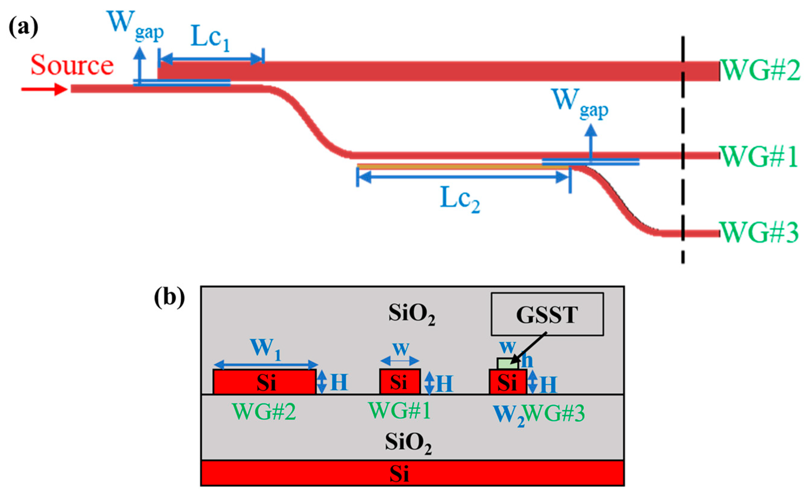
Figure 1 shows the structure of the multi-functional integrated optical switch. The proposed optical switch was manufactured on a 220 nm-thick (
) SOI platform covered with silica (SiO
2). It consisted of two asymmetric directional couplers, one of which had a waveguide loaded with GSST and one waveguide of the two directional couplers was common.
In this paper, we chose popular SOI waveguides with a
-thick silicon core layer and a
-thick buried silicon dioxide layer. When the central wavelength was 1550 nm, the refractive index of the silicon and silica were
and
, respectively [
21]. According to [
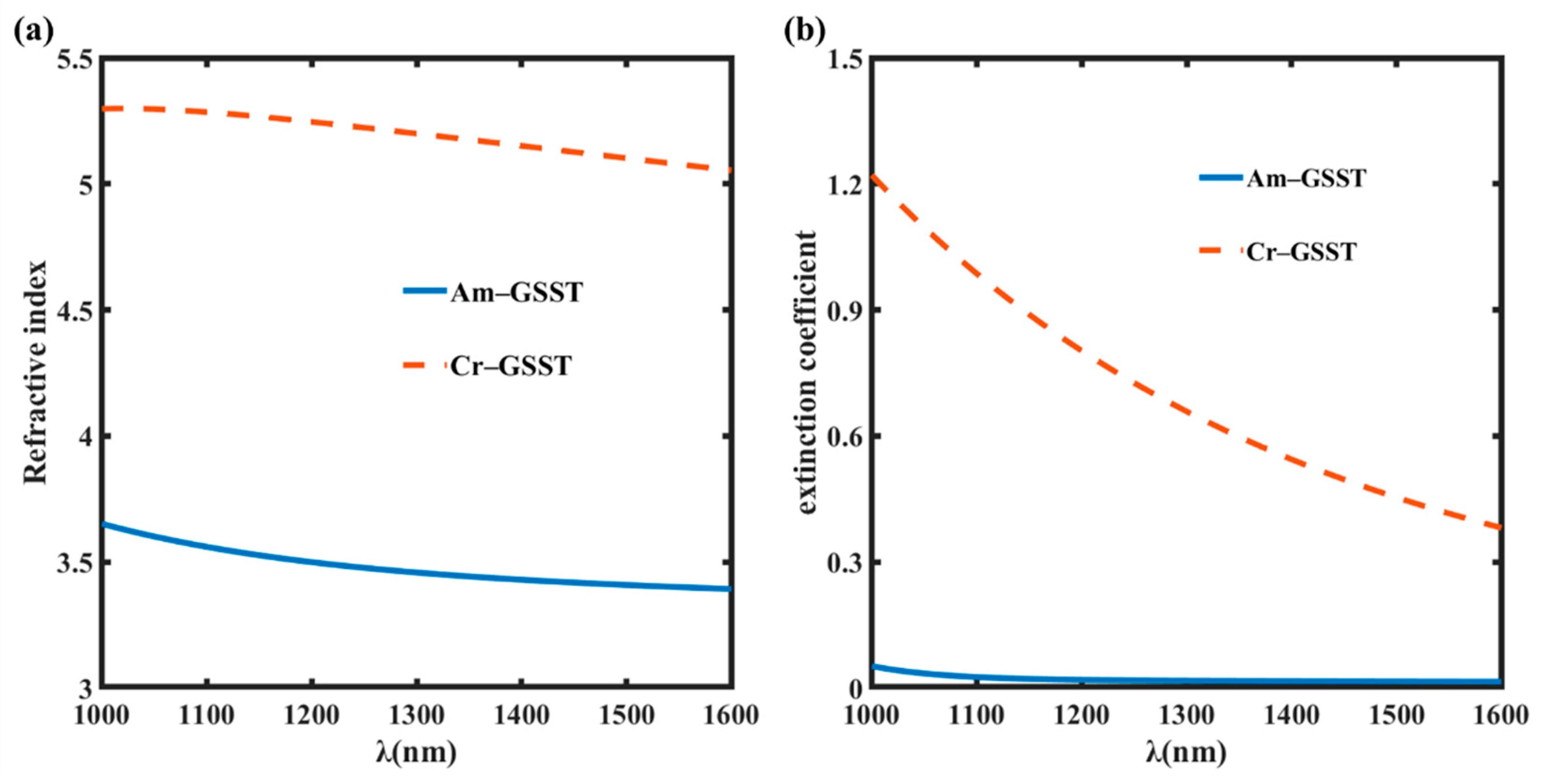
31], the complex refractive index of GSST in an amorphous state is
and in a crystalline state it is
(as shown in
Figure 2). In order to facilitate the processing, all silicon waveguides took the same height:
was the size of the common waveguide (WG#1);
was the size of another waveguide (WG#2) of the directional coupler without a GSST load;
was the size of another waveguide (WG#3) of the directional coupler loaded with GSST; and
was the size of GSST of the load. The distance between the adjacent waveguides was
(the distance was also set to
for easy processing) and the coupling lengths of the directional couplers with unloaded and loaded GSST were
and
, respectively.
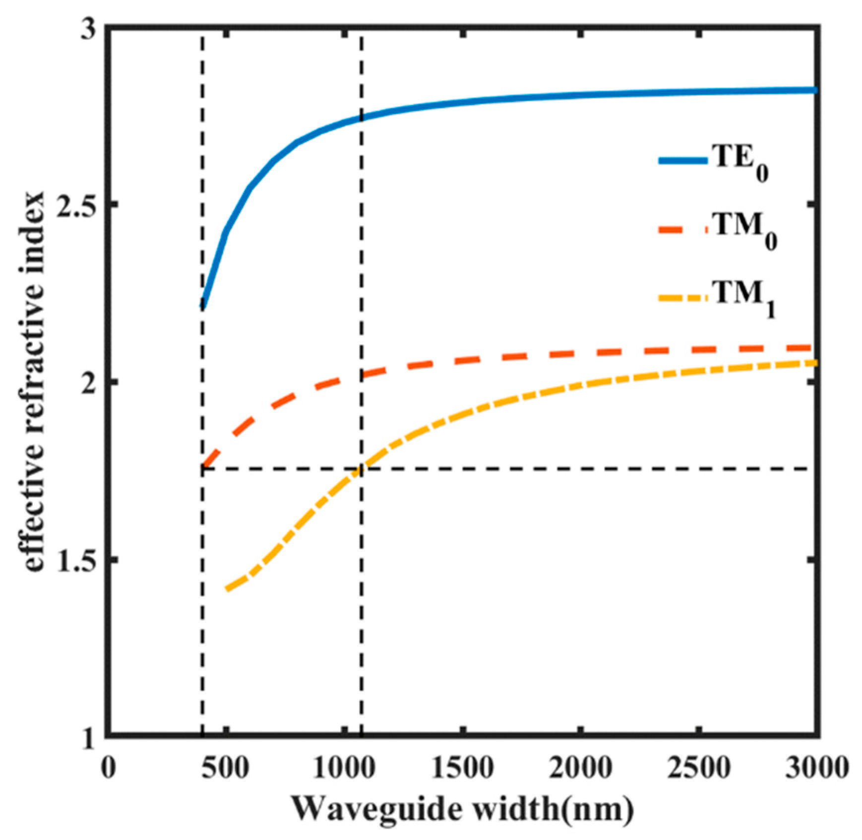
By selecting an appropriate waveguide width, the TM
0 and TE
0 modes of waveguide WG#1 incident were separated. The TM
0 mode was converted to the TM
1 mode by the asymmetric directional coupler and was output by waveguide WG#2. When GSST was amorphous, waveguide WG#1 and waveguide WG#3 of the directional coupler based on GSST were phase matched and the TE
0 mode was coupled from waveguide WG#1 to waveguide WG#3. However, when GSST was crystalline, the TE
0 mode was output from waveguide WG#1 due to the phase mismatch and the coupling was ignored. When the phase matching condition
was satisfied, the higher-order modes could be excited where
and
were the effective refractive indexes of the fundamental mode of the input single-mode waveguide and the
i-order mode of the multi-mode waveguide, respectively [
32]. Therefore, the width of the multi-mode waveguide was appropriately selected to achieve the coupling between the TM
0 mode and the TM
1 mode. Similarly, when GSST was amorphous, to achieve the coupling of the TE
0 mode from waveguide WG#1 to waveguide WG#3, phase matching condition
was required where
and
were the effective refractive indexes of waveguide WG#1 and waveguide WG#3, respectively.
Figure 3 shows the effective refractive index of the eigenmode in the SOI waveguide as a function of the waveguide width. When a common waveguide width of the two directional couplers was selected as
and the spacing was
, according to the phase matching conditions and continuous parameter optimization it was determined that the widths of waveguide WG#2 and waveguide WG#3 were
and
, respectively. The size of the loaded GSST was
.
Using the super-mode theory [
33],
, the coupling length of the coupling region of the two directional couplers was roughly calculated at first where
βe and
βo were the propagation constants of the even mode and the odd mode, respectively. The full-vector three-dimensional finite-difference time-domain (3D-FDTD) method was then used to further optimize the coupling length. Finally, the coupling lengths were determined as
and
, respectively. The parameters optimized in this paper included the waveguide width, GSST width/thickness, and the coupling length. The other parameters mainly served for the parameter optimization of the coupling length. To ensure phase matching, the effective refractive indices of the two waveguides were required to be the same. When the main waveguide width was determined, the selected width of the waveguide without loaded GSST was 1030 nm; for the waveguide with loaded GSST, and because the refractive index of GSST is higher than Si, in order to fulfil the phase matching condition, the corresponding waveguide width was less than the width of the main waveguide. There were several other parameters measured (including the width of the silicon waveguide loaded with GSST and the width and thickness of GSST), but, for brevity, we only report the most notable results that supported our conclusion in this paper.
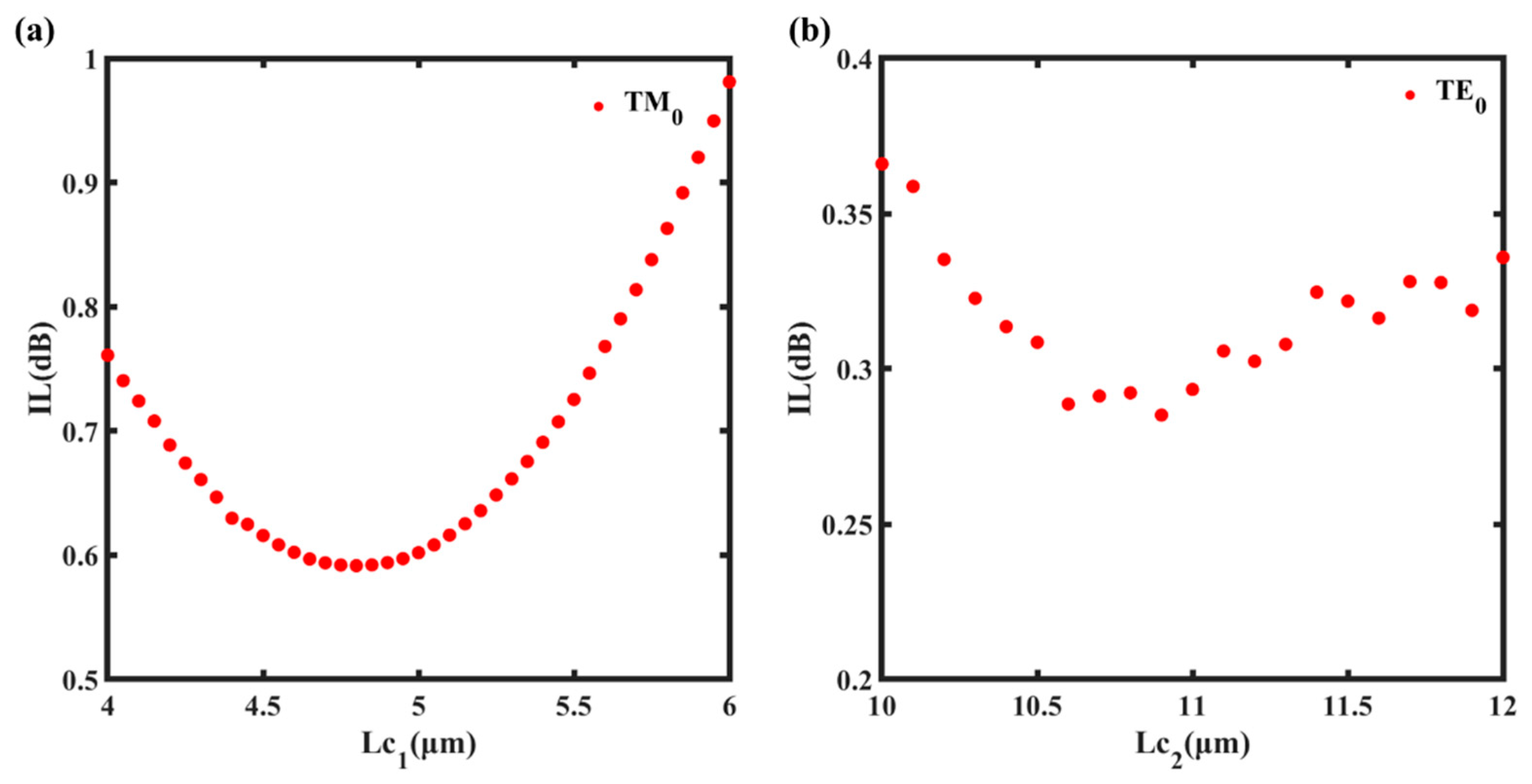
Figure 4 shows the coupling degree C of the directional coupler varies with the length of the coupling region (the C was defined as the ratio of the output optical power of the coupling port to the input optical power, the lower the C, the stronger the coupling). It should be noted that this was the computational optimization of splitting the device into two separate directional couplers (GSST-loaded and GSST-unloaded). For the directional couplers without GSST loading, the coupling of the TM
0 mode to the TM
1 mode was mainly discussed. For the GSST-loaded directional couplers, the coupling was discussed when the TE
0 mode was input and GSST was in an amorphous state. Finally, we combined the coupling lengths Lc
1 and Lc
2 and obtained a final value of the coupling length through a continuous optimization.
Thus, the structural parameters of the multi-functional integrated optical switch were basically determined; the details are given in
Table 1.
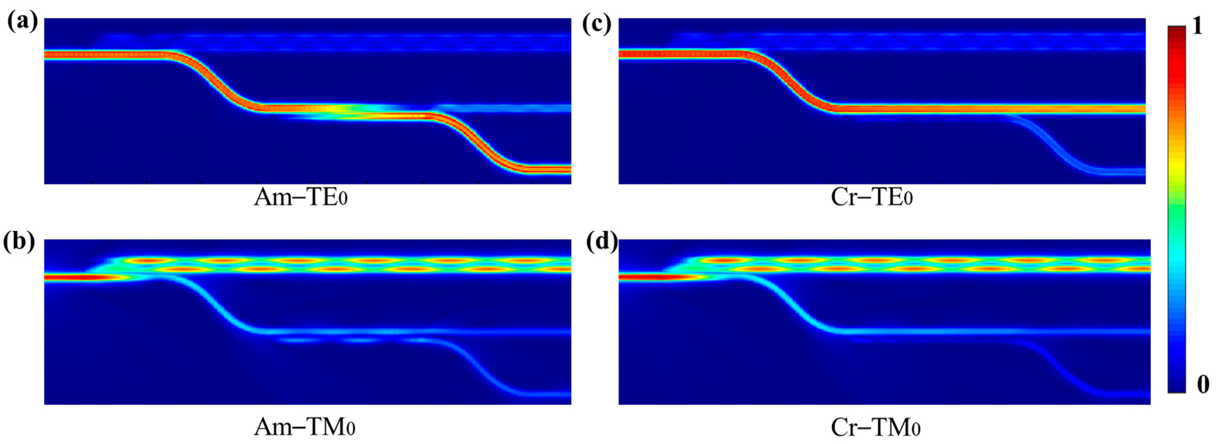
As shown in
Figure 5, the light field distribution of the TE
0 mode and the TM
0 mode input at a wavelength of 1550 nm when GSST was in an amorphous or crystalline state was simulated. It was found that when the TM
0 mode entered the common waveguide of the two directional couplers, GSST was either amorphous or crystalline and the light was coupled from waveguide WG#1 to waveguide WG#2; few parts of the TM
0 mode were output from waveguide WG#3. When the TE
0 mode was inputted and GSST was amorphous, most of the TE
0 mode was coupled to waveguide WG#3 and a small part was output by the other waveguide ports. Conversely, when the TE
0 mode was input and GSST was crystalline, few parts of the TE
0 mode were coupled to waveguide WG#2 and waveguide WG#3; most of them were directly output by waveguide WG#1.
3. Discussion
The induction methods of phase change materials mainly include thermal induction and optical induction. The realization principle is to heat up the phase change materials by means of external electrodes or by pumping light to reach the threshold temperature of the phase change. At present, the main methods of inducing phase change materials in on-chip optical devices are external ITO (indium tin oxide) electrodes [
34] and external laser induction [
35,
36]. In the design of an electrical induction scheme, the reason for using an ITO electrode is not only to induce the phase transformation of the phase change materials via a high temperature, but also to prevent the oxidation of the phase change materials in air, playing a protective role. In the design of an external laser induction scheme, the crystallization ratio of amorphous phase change materials can be adjusted by changing the heating temperature, heating time, or laser pulse intensity to obtain different refractive indexes, which is more convenient to control the crystallization degree of the phase change materials.
Our designed optical switch structure was thermally simulated by COMSOL and the feasibility of using laser heating to induce the phase transition of GSST was studied. By referring to relevant references [
37,
38,
39,
40,
41], the thermal coefficients of GSST, Si, and SiO
2 were obtained; the results are shown in
Table 2.
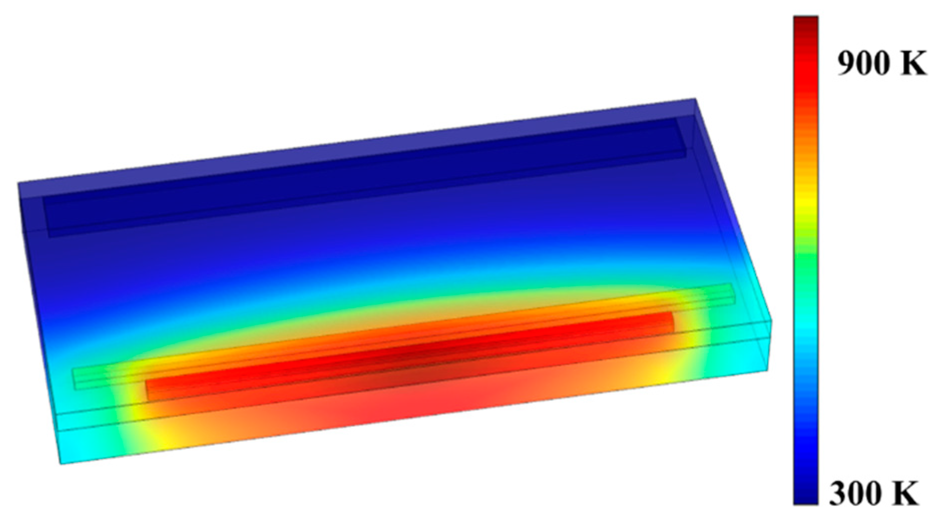
The transition of GSST from a crystalline to an amorphous state requires a short pulse of high energy to exceed a melting temperature of 900 K and then rapid cooling to change the atomic arrangement from ordered to disordered. The transition from an amorphous state to a crystalline state requires a long pulse of low energy, slowly heating the temperatures above 523 K and below 900 K for a period of time to change the atomic arrangement from disordered to ordered.
The switching time was simulated by studying the process of GSST from a crystalline state to an amorphous state. For the real thermal simulation, a 500 nm SiO
2 covering layer was used on the waveguide and the coupling part of the designed device was taken. On the top of the device, a high-energy gaussian short pulse was input to provide heat; the pulse width was set to 25 ns and the grid selection was extremely elaborate. When the input spot radius was 6 μm, the power was 10 W; the temperature distribution when the pulse duration reached 20 μs is shown in
Figure 6. It can be seen from the figure that the temperature of GSST exceeds 900 K, reaching a phase transformation condition. The temperature of the bottom silicon waveguide and the silicon dioxide base part was below 900 K. It should be noted that the long switching time was due to the low peak power of the selected laser. If the power was too high, the device quickly reached the required temperature, but it increased the difficulty of temperature control.
The performance of a waveguide depends on losses. The losses in the waveguide depend on the materials, wavelength, and fabrication method used. The bend loss can be reduced using LPCVD and TriPlex LPCVD technology. When the bending radius was larger than 3 μm, the loss was 2–3 dB/cm. One of the other losses originated from the inner wall roughness of the waveguide. Roughness can greatly increase light scattering, leading to a significant light transmission loss. Fabrication-caused surface roughness is inevitable because it is a result of the intrinsic noise in the lithography and etching processes. Using SPEL, the average sidewall roughness of a silicon waveguide can be reduced from 13 to 3 nm. Therefore, the loss caused by the roughness of the inner wall and bending of the waveguide can be effectively avoided.
The performance parameters IL, CT, and ER were also discussed.
First, the IL was defined as the ratio of the output optical power to the input optical power; the lower the IL, the better the performance of the optical switch:
The
CT was then defined as the ratio of the output power of the conduction port of the optical switch to the output power entering the adjacent port; the lower the
CT, the better the performance of the optical switch:
Finally, the ER was defined as the ratio of the optical power when the optical switch was in an on state and the optical power when the optical switch was in an off state; the lower the ER, the better the performance of the optical switch:
where
is the transmission of the input mode, whether the TE mode or the TM mode was input.
,
, and
were the transmissions of mode light passing through waveguide WG#1, waveguide WG#2, and waveguide WG#3, respectively.
,
, and
were the transmissions of mode light passing through waveguide WG#1, waveguide WG#2, and waveguide WG#3, respectively, when GSST was amorphous.
,
, and
were the transmissions of mode light passing through waveguide WG#1, waveguide WG#2, and waveguide WG#3, respectively, when GSST was crystalline. The performance parameters of the optical switch, IL,
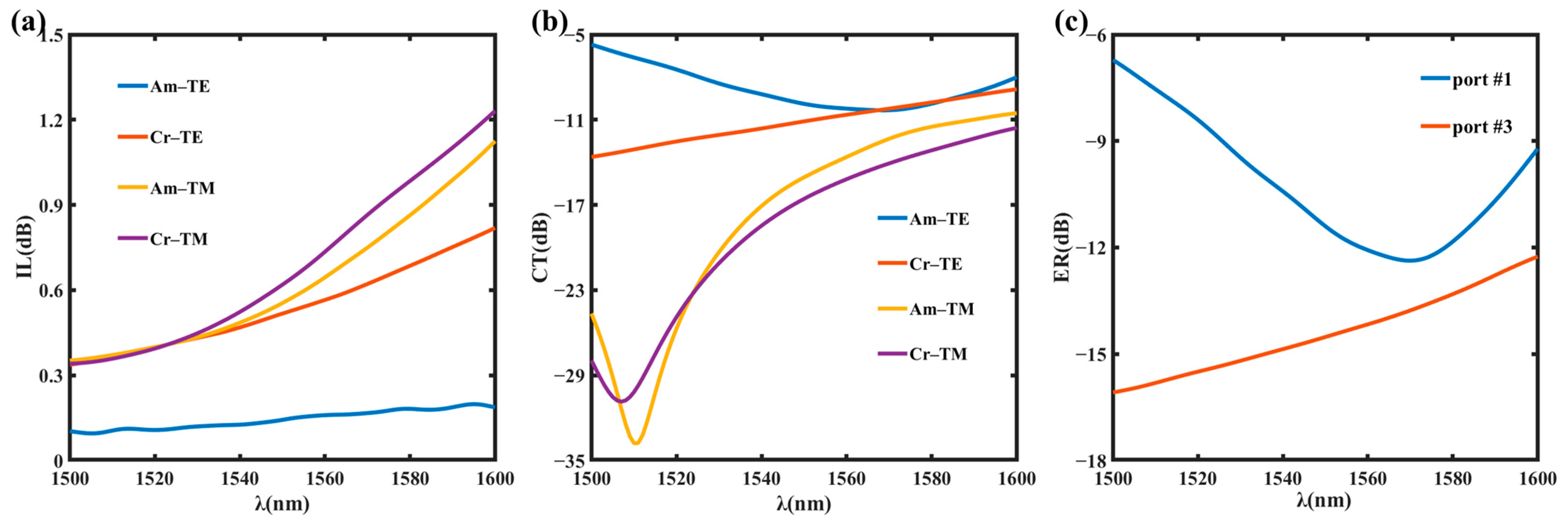
CT, and ER changed with the wavelength, as shown in
Figure 7. The IL and
CT analyzed the input of the TE mode and the TM mode, respectively; the ER only considered the incident of the TE mode. This was because the definition of the extinction ratio and optical switching function was mainly realized by the TE mode controlled by GSST through the directional couplers loaded with GSST.
Figure 7a,b shows four curves labeled “Am–TE”, “Cr–TE”, “Am–TM”, and “Cr–TM”, which refer to the cases where GSST was amorphous and the TE mode was input, GSST was crystalline and the TE mode was input, GSST was amorphous and the TM mode was input, and GSST was crystalline and the TM mode was input, respectively. Regarding the ER, we only discussed the case of the TE mode input. In the analysis figure of extinction ratio, “port #1” and “port #3” referred to waveguide WG#1 and waveguide WG#3 as the output, respectively; unlike the former two, the optical power output by waveguide WG#2 was not calculated.
When the wavelength was 1550 nm, the IL was lower than 0.62 dB in the case of the TE0 mode and the TM0 mode input, regardless of whether GSST was amorphous or crystalline; when only the TE mode incident was considered, the IL was 0.14 dB when GSST was amorphous and 0.52 dB when GSST was crystalline. Moreover, with the increase in wavelength, the increasing IL indicated that the total optical power at the output was decreasing, which was because the extinction coefficient spectrum of GSST decreased. When the TE0 mode was input and the wavelength was 1550 nm, the CT was −9.88 dB in the amorphous and −11.40 dB in the crystalline GSST. When the TE0 mode was input and the wavelength was 1550 nm, the ER of waveguide WG#1 was also lower than −11.40 dB and the ER of waveguide WG#3 was lower than −14.52 dB.
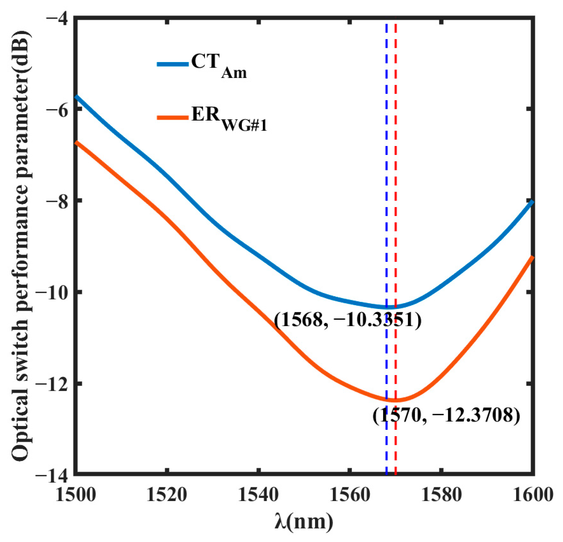
From
Figure 8, it can be seen that when the TE mode was input, the
CT first decreased and then increased with the increase in wavelength and reached the lowest value at 1568 nm when GSST was in an amorphous state, which was −10.34 dB; the ER of waveguide WG#1 first decreased and then increased with the increase in wavelength and reached the lowest value of −12.37 dB at the wavelength of 1570 nm. The ER of “port #1” refers to the ratio of the optical power when “port #1” was in an on state and when it was in an off state. The two were given by the following formulas:
It was found that the two formulas were mainly determined by
. This was because the optical power entering waveguide WG#2 was negligible compared with the optical power entering waveguide WG#1 and waveguide WG#3 when the TE mode was input.
and
refer to the transmission of mode light passing through “port #3” when GSST was amorphous and the transmission of mode light passing through “port #1” when GSST was crystalline, respectively. These refer to the transmission when “port #3” and “port #1” were in an open state and both reached a lowest value (1568 nm and 1570 nm, respectively) when close to 1550 nm (as shown in
Figure 8), which further demonstrated that the performance was better when it was close to 1550 nm. As the designed optical switch mainly worked at 1550 nm, the closer the wavelength was to 1550 nm, the better the coupling effect; thus, the output power of waveguide WG#1 was lower and the crosstalk and extinction ratio were smaller.
Similarly, when the TE mode was input, the CT increased with the increase in wavelength when GSST was in a crystalline state; the ER of waveguide WG#3 increased with the increase in wavelength. The ER of “port #3” refers to the ratio of the optical power when “port #3” was in an on state and when it was in an off state. This same trend was because, with the increase in wavelength, the refractive index of GSST became smaller, resulting in a smaller equivalent refractive index between the waveguides. Thus, more light was coupled to waveguide WG#3, so and became larger with the wavelength.
For the obtained simulation results, in order to facilitate the performance analysis of the simulation results, the 1 × 2 optical switch designed in this paper was compared with 1 × 2 optical switches designed in other references, all of which were theoretical. The phase change material used in references [
5,
41] was GSST and only the incident situation of the TE mode was discussed. However, the incident situation of both the TE mode and the TM mode was discussed in reference [
42].
Table 3 shows the results of the comparison. It should be noted that “Cross-State” in
Table 3 refers to the situation when the TE mode was input and GSST was amorphous and “Lower” refers to the lower performance parameters whether GSST was amorphous or crystalline when the TM mode was input.
It can be seen from
Table 3 that references [
5,
41] both had a low loss and small size for the TM mode. It can be seen from
Figure 3 that, with the increase in waveguide width, the effective refractive index of the TM mode changed less than the TE mode. Therefore, the structures set in the two literature examples could not meet the optical switching functions of the TE mode and the TM mode at the same time. For the TM mode, the corresponding coupling region should be separately designed. However, although reference [
42] discussed both the TE mode and the TM mode, the device size was large. Compared with references [
5,
41], the advantage of our work was mainly reflected in the situation when the TM mode was input without increasing the device size. Compared with reference [
42], the advantages were mainly reflected in the lower IL when the TE mode was input and the device size was one-fifth of the device size in reference [
42]. Compared with the other references, the crosstalk needed to be further reduced. We considered changing the radius of the bent waveguide or changing the structure of the waveguide that implemented the polarization beam splitting and mode conversion functions to reduce the crosstalk by shortening the length/width of the device. Regarding changing the radius of the bent waveguide, because bend waveguides can be divided into four categories according to their different geometric shapes (sine bend (Sin_Bend), cosine bend (Cos_Bend), double arc-type (S_Bend), and double arc middle plus straight waveguide-type (SB_Bend)), the cosine-type waveguide had the lowest loss by comparing the losses between the various types of curved waveguides; thus, changing the curved waveguide part of the designed optical switch to a cosine curved waveguide could be tried [
43]. Regarding changing the structure of the waveguide, we considered two methods that could be used. One of the methods was a wider ridge waveguide to reduce transmission loss. For the ridge waveguide, the mode field overlapped less with the side wall of the waveguide, so the influence of the side wall was relatively small. The transmission loss of the waveguide could be greatly reduced and the transmission loss of the ridge waveguide based on shallow etching could reach 0.3 dB/cm [
44]. The other method was a SiN waveguide used to transfer the light from the Si waveguide to the SiN waveguide. The refractive index of SiN is smaller than that of Si, so the light field binding was weak and the loss caused by the side wall roughness was relatively small [
45].


