Communication

A Multi-Layered Borophene-Silica-Silver Based Refractive Index Sensor for Biosensing Applications Operated at the Infrared Frequency Spectrum

by
Abdullah G. Alharbi
1,
Vishal Sorathiya
2,* and
Sunil Lavadiya
2
1
Department of Electrical Engineering, Jouf University, Sakaka 42421, Saudi Arabia
2
Department of Information and Communication Technology, Marwadi University, Rajkot 360002, India
*
Author to whom correspondence should be addressed.
Photonics 2022, 9(5), 279; https://doi.org/10.3390/photonics9050279
Submission received: 6 March 2022 / Revised: 14 April 2022 / Accepted: 18 April 2022 / Published: 20 April 2022
(This article belongs to the Special Issue Light-Based Smart Technologies for Biomedical Sensing and Imaging)

Abstract

:
We have presented the borophene based refractive index sensor for the infrared frequency spectrum of 188 to 250 THz (1.2–1.6 µm) range. The proposed structure was formed by using the Silver-borophene-silica-Ag layered structure. The behaviour of the different analyte (with a different refractive index) material is numerically calculated by placing it on the top of the structure. The behaviour of the structure is identified in terms of absorption, reflectance, physical parameter variation, and oblique angle incident conditions. The presented results provide the basic idea of selecting optimized structure dimensions to get the specific resonating response. This sensor offers the Figure of Merit (FOM) of 444 RIU−1 with high sensitivity of 660 THz/RIU (4471 nm/RIU). The refractive index sensor also provides wide-angle stability for (0° to 80°) for the wide frequency range (239 to 245 THz and 207 to 209 THz). This sensor is developed on the silver metal layer (not required to separate borophene from its origin metal deposition process) and easily fabricated using standard boron fabrication and layered deposition techniques. The results of the proposed structure make it possible to design a basic biosensor structure. This device is also applicable for various THz and biomedical applications.

1. Introduction

Research into two-dimensional (2D) materials is brisk due to the possibility of their implementation into next-generation electrical and energy conversion devices [1,2,3,4]. Scientists across the globe are buzzing about an entirely new kind of two-dimensional material, known as borophene (also known as a two-dimensional (2D) boron sheet), which was recently successfully synthesized on single crystal Ag(111) substrates under ultrahigh-vacuum conditions [5]. Scanning tunnelling spectroscopy experiments show that borophene exhibits anisotropic metallic behaviour in its crystal structure. Like borophene material, graphene is a zero-gap semiconductor with linear dispersion at the Dirac points in its electrical characteristics. Because of this, g charge carriers of graphene act like Dirac fermions with no mass [6]. Graphene is a very efficient material due to its low absorption of visible light and high carrier mobilities [7,8]. Graphene might be used as a transparent conductor in various applications. The advantages of graphene-like weight, durability, and flexibility outweigh the standard ITOs (Indium tin oxide). Researchers have been inspired to further investigate the controlling light-matter interactions because of the high electron density and significant anisotropy of borophene. Patterned borophene has been shown to display anisotropic plasmonic activity at visible wavelengths based on the plasmon modes of other 2D materials [7,8].
Furthermore, it is predicted that borophene contains extraordinary mechanical properties comparable to graphene [5]. Due to the distinct characteristics of 2D materials in comparison to their bulk counterparts, research on their layered topologies for future device manufacturing is being pursued [9,10]. The characteristics of recently manufactured graphene, silicene nanosheets, boron-nitride nanosheets, transition-metal dichalcogenides (TMDs), and black phosphorus [1,9,11,12,13] are distinct from or superior to those of their bulk counterparts. Research into layered materials with unique characteristics is a thriving field of study, owing to the relevance of the subject matter in science and the potential for practical applications. The change from an indirect semiconductor in bulk to a direct semiconductor in a monolayer [14] in several layered metal dichalcogenides (e.g., MoS2), for example, has sparked interest in the optoelectronic capabilities of these materials.
In recent years, two-dimensional materials and optical biosensors have been one of the most growingly important researched topics. In addition to graphene, transition metal dichalcogenides, black phosphorus, and MXenes, a broad range of 2D materials display unique optical properties and may be utilized to detect a wide range of biomolecules, according to the researchers. Optical biosensor sensitivity and detection limit have been greatly improved over traditional sensors (such as electrical sensing) due to the change in 2D materials [15]. Traditional gas sensors, such as carbon nanotubes and graphene, are susceptible to a wide range of unpleasant gases, but they cannot detect more harmful molecules like formaldehyde, which may cause cancer and other health problems. In recent years, borophene’s wide variety of gas sensor applications has generated much attention. The DFT-based (Density-functional theory) study of borophene nanometers as formaldehyde sensors has been underway. As a result of previous successes with bending and linear borophene defects in the preparation phase of 2D borophene command on the molecular adsorption ability of NO (Nitrogen oxide) gas, scientists are now using these findings to develop new and improved 2D borophene command formulations. For example, when nano-sized borophene is absorbed into an alcohol solution, the bandgap decreases fast, thus increasing conductivity. Consequently, adsorption energy and bandgap fluctuations may be used to detect ethanol vapour [16].
Many more 2D materials are now being investigated. Multi-layered borophene is one of the most exceptional materials in this category. An investigation of the optical characteristics of monolayer borophene has been conducted. However, when examining multi-layered borophene, there is still a dearth of scholarly material to draw upon. As borophene has a highly anisotropic structure, the electrical and magnetic properties may be changed, allowing for a wider range of applications [17,18]. According to the authors, achieving an ideal combination of these features would be the most challenging problem in future applications. It is necessary to reduce photon absorption and reflection while preserving high electrical conductivity and transparency, for example, in the development of intelligent windows [19,20]. Borophene electrical and optical features must be thoroughly studied for possible usage in future devices. The biosensor structure works on the principle of perfect absorption, transmittance, and reflectance. The layered structure of different metal structures is the primary requirement to trap infrared light and generate the perfect absorption [21,22] and reflectance [23]. The perfect absorption/reflectance-based multilayer device can be useful for designing biosensor structures [24]. To achieve the perfect absorption/reflectance, the dimension and shape of the resonator structure play a major role in the device’s overall performance [25,26,27,28]. This structure is analysed over an infrared frequency of 1.2 to 1.6µm, the third optical window of communication. Major optical fibre-based sources and receivers are available for overall system setup in this spectrum. This sensor is applicable for designing infrared biosensors for detecting haemoglobin [29,30], urine, water, ethanol, Glucose [31], Biotin Streptavidin and Fibrinogen. The refractive index of these materials fall between 1 to 1.7 [23,25,32].
In this article, we have proposed borophene based photonics devices for refractive index sensing applications. We have formed the multi-layered metal-borophene-silica and silver layered structure to generate the resonance effect at the infrared frequency range. The proposed structure is numerically investigated using FEM (Finite element method) computational technique provided by the COMSOL Multiphysics simulator environment. The behaviour of the refractive index sensor is investigated in terms of absorption, reflectance, physical parameter variation and sensitivity variation.

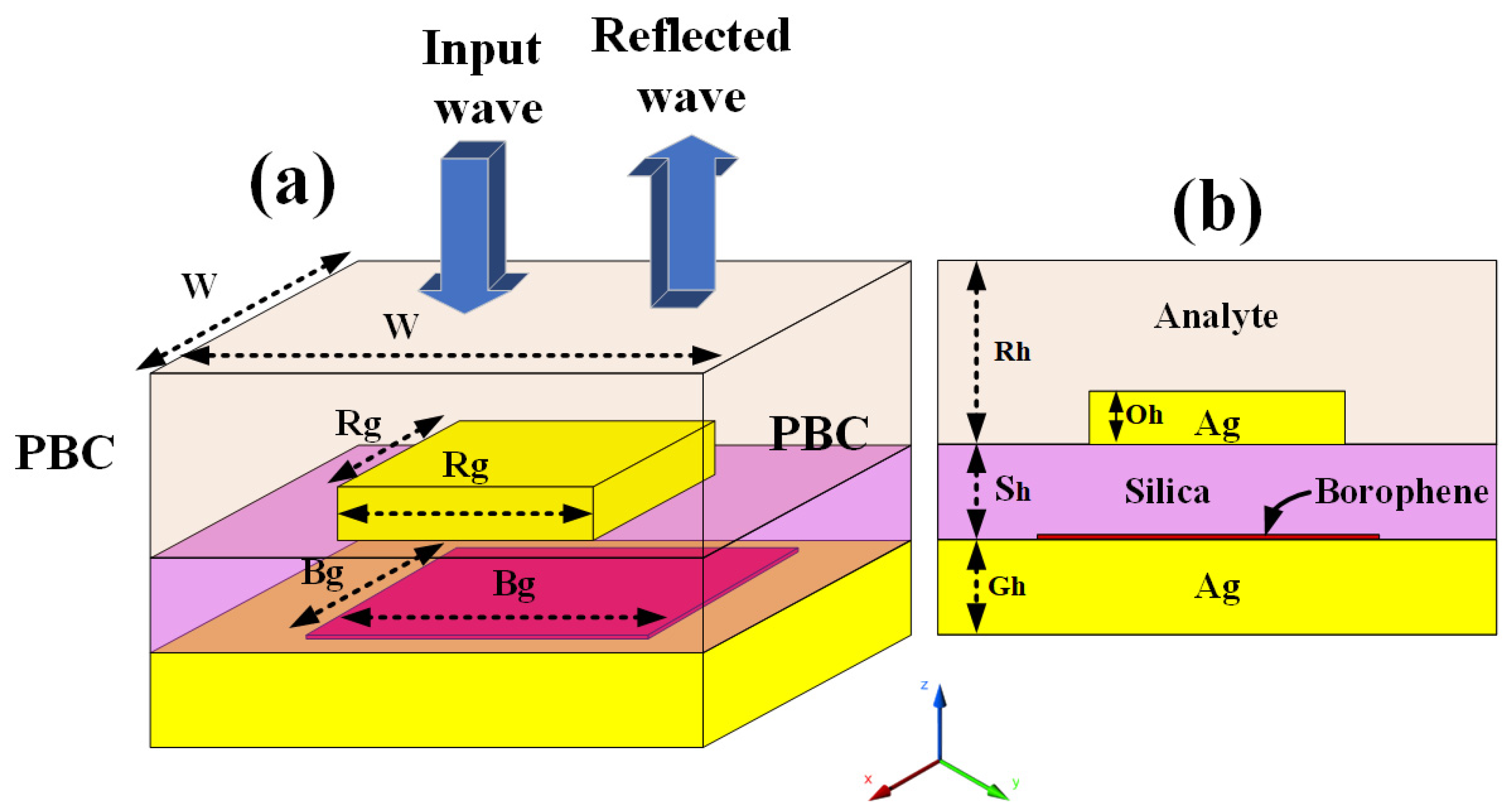
2. Borophene Based Biosensor Structure

The schematic of the borophene based biosensor is shown in Figure 1. Figure 1a,b show the proposed structure’s three-dimensional and side view. The bottom layer of the structure is set as silver material. No measurements of the monolayer optoelectronic properties have been made since no freestanding borophene has been separated. The influence of an Ag(111) substrate on the electrical structure of borophene is more complex [33] than that of graphene. However, borophene adsorption on silver surfaces has a metallic property [5,34]. Freestanding borophene allotropes are predicted to have 2D metals with a wide variety of electrical properties based on ab initio calculations and experimental data. For example, DFT has demonstrated that the electronic band structures of the many borophene allotropes are remarkably diverse [35,36,37]. A quadratic or a typical metal structure may be seen in the band structure at Fermi energy, even though all 2D allotropes are metallic. Several allotropes may affect this.
Chemical vapour deposition, bottom-up fabrication, top-down methods, liquid-phase exfoliation, and sonochemical procedures have been used to thin borophene atoms. Exfoliation of borophene nanolayer bulk B is very difficult, which severely restricts its use in the future [16,38]. The borophene individual layer is still a major fabrication challenge, but the single-layer graphene can be formed on different metal substrates like Gold, Copper and silver [39,40,41] to realize the nanostructure photonics devices. It is possible to form the single-layered borophene on the silver substrate layer as the method suggested for borophene formation in [38]. The chemical stability of borophene is less stable than that of other 2D materials, and it is more vulnerable to contamination when exposed to air for an extended period. While lower than graphene, chemical stability helps solve the problem of oxidative instability in 2D materials that had previously been intractable. The researchers also discovered new ways to improve borophene stability against oxygen, such as coating it with another substance to shut it off from exposure to oxygen. It encouraged us to investigate the oxidation resistance of 2D boron further, which they revealed could be greatly reduced by using a silicon/silica oxide capping layer [42]. Lithography or laser beam lithography techniques can form the top layer of gold. The proposed structure is formed with the multiple layers of the silver-borophene-silica-silver, as shown in Figure 1b. The dimensions of the overall structure are set as: W = 1.8 µm, Rg = 900 nm, Bg = 900 nm, Rh = 2 µm, Sh = 800 nm, Gh = 400 nm, Oh = 200 nm. The dimension of the structure is chosen by considering the patch size of the borophene material. The dielectric constant of Ag material is considered from the constant optical value suggested in [43]. This sensor is analysed in the frequency range of 1.2 to 1.6 µm (180 to 250 THz).
The dimension of the overall structure is set <1.6 µm (W = 1.8 µm) to create the patch geometry on the bottom Ag layer. This patch dimension of borophene generates the dipole moment across the edge of the borophene layer, resulting in resonating conditions. The proposed structure was numerically investigated using COMSOL Multiphysics simulation software [44]. The boundary conditions of the structure are set as a periodic (Periodic boundary condition- PBC) over the X-Y plane. The wave was inserted from the top of the structure (Z -direction), presenting refractive index material. The absorption conditions are set as A = 1 − R. A reflectance value is zero because of the silver resonator at the bottom of the structure. It leads us to calculate all the results from absorption. However, the reflectance coefficient gives us the opposite results of the overall structure, making it flexible in analysing results by reflectance or absorption. It is observed from Figure 1 that in consideration of reflectance results, this whole study can be verified by converting those results into absorption by using a formula of A = 1 − R. Reflectance coefficient is identified from the S11 parameter. Minimum and maximum meshing sizes are set as 0.5 nm and 50 nm. The meshing growth rate is set to the factor 1.3. Borophene dielectric equation [16] can be defined by the equation shown in Equation (1). This equation determines the optical properties under the consideration of only intraband transition because the interband transition calculation for low frequency cannot be accurate. The real part and imaginary part of the borophene dielectric function can be defined as shown in Equation (2) ( ε r e a l α β ( ω ) ) and Equation (3) ( ε i m a g i n a r y α β ( ω ) ). The modified equation of imaginary modified after median tensor [16]. Here ε r e a l α β ( ω ) is obtained from the Kramers-Kronig formula.
ε ( ω ) = ε 1 ( ω ) + i ε 2 ( ω )
ε i m a g i n a r y α β ( ω ) = 1 + 2 π P 0 ε 2 α β ( ω ) ω ω 2 ω 2 + i η d ω
ε r e a l α β ( ω ) = 1 + ( 2 / π ) P 0 ( ε 2 α β ( ω ) ω / ω 2 ω 2 + i η ) d ω
ε 2 α β ( ω ) = 2 π e 2 Ω ε 0 k , v , c δ ( E k c E k v h ω ) | Ψ k c | u · r | Ψ k v | 2
L ( ω ) = lm ( 1 ε ( ω ) ) = ε 2 ( ω ) ε 1 2 ( ω ) + ε 2 2 ( ω )
α ( ω ) = 2 ω c { [ ε 1 2 ( ω ) + ε 2 2 ( ω ) ] 1 / 2 ε 1 ( ω ) } 1 / 2
R ( ω ) = | ε 1 ( ω ) + i ε 2 ( ω ) 1 ε 1 ( ω ) + i ε ( ω ) + 1 | 2
Here, ε 0 is the vacuum dielectric constant, e is the electron charge, Ω is volume, and h is a plank constant. Ψ k v express the valance band ( v ) and Ψ k c Conduction band ( c ) at the momentum value of u r at point k . ω is the energy of the phonon. P denoted the principal values in the Kramers-Kronig formula. The borophene dielectric loss ( L ( ω ) ) , absorption ( α ( ω ) ) and reflectance constant ( R ( ω ) ) can be calculated using the equation shown in Equations (3)–(5), respectively. Furthermore, the borophene dielectric constant for the visible and infrared range can be presented [16]. The dielectric equation and electron energy loss equation of incoming radiation is validated by polarising the electric field vector E in the directions of a and b. The anisotropic crystal structure of borophene leads to anisotropy in its optical and thermal conductivity characteristics. We have articulated the borophene as impedance boundary conditions in COMSOL. The dielectric constant values for the borophene are taken from the eV versus dielectric constant graph as shown in [16,38].

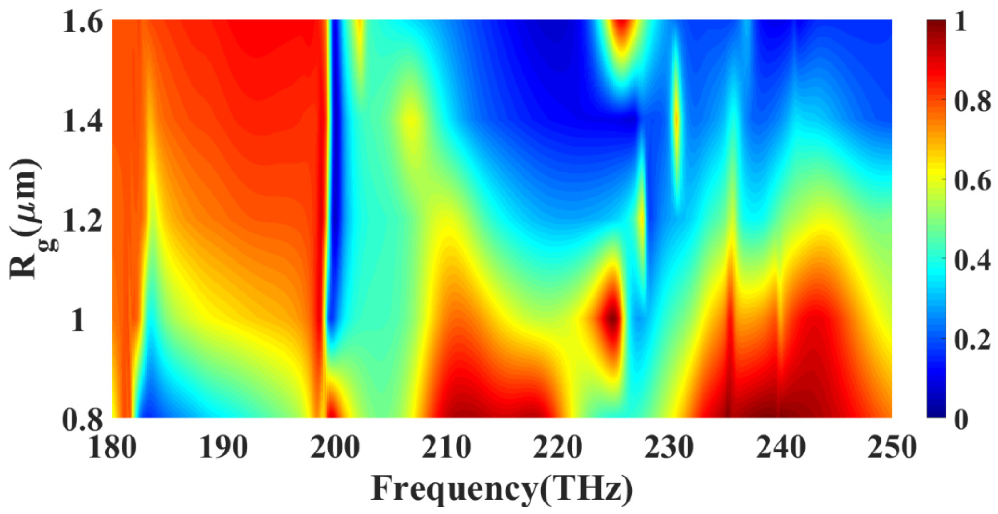
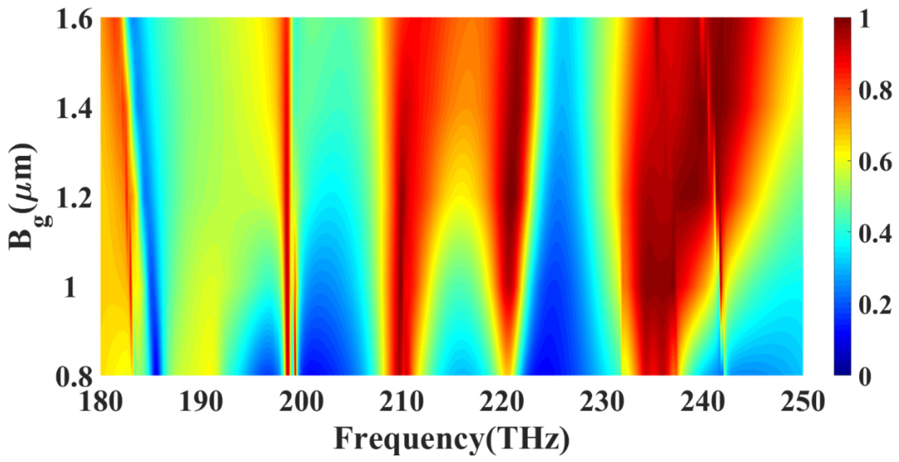
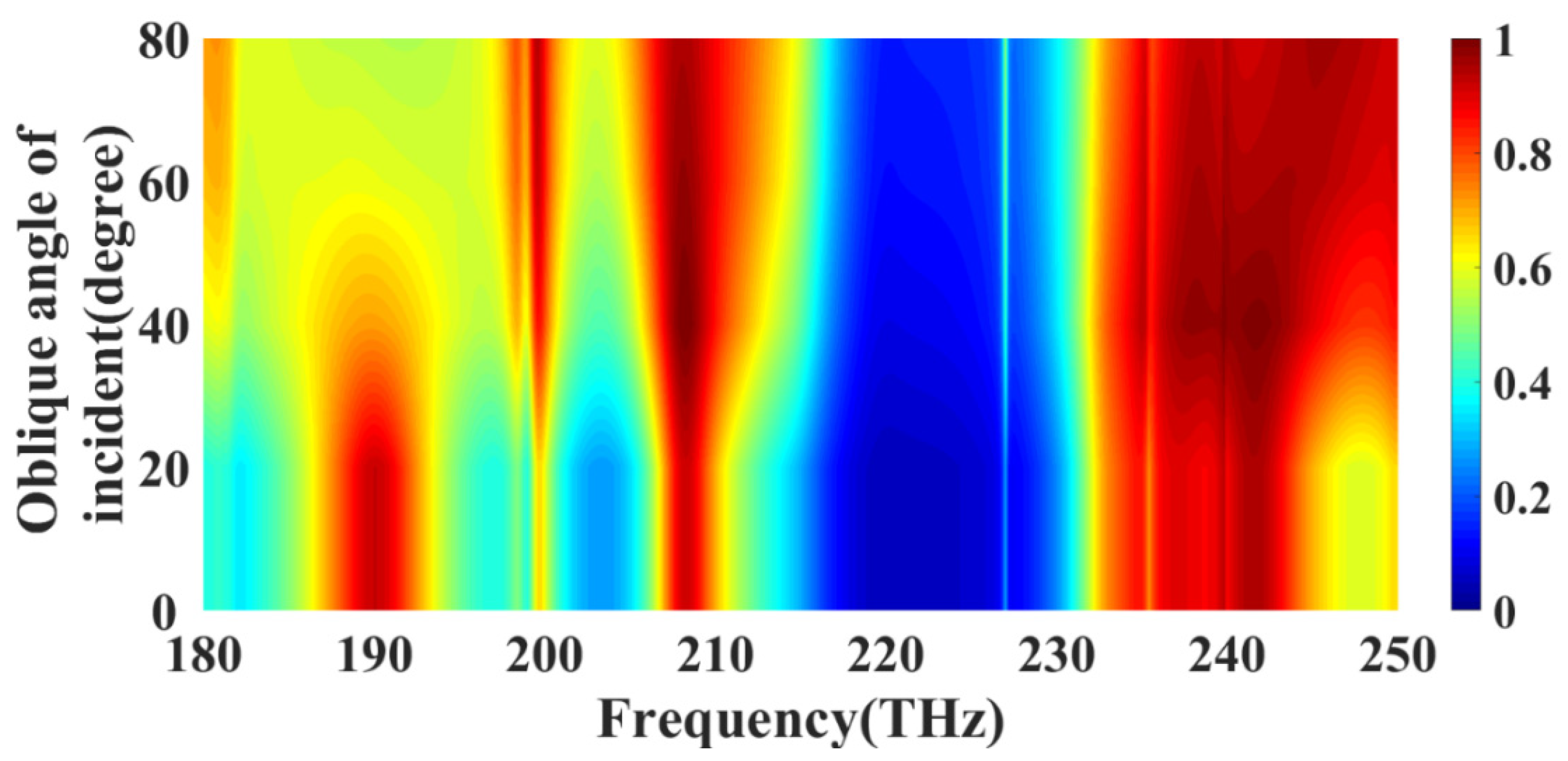
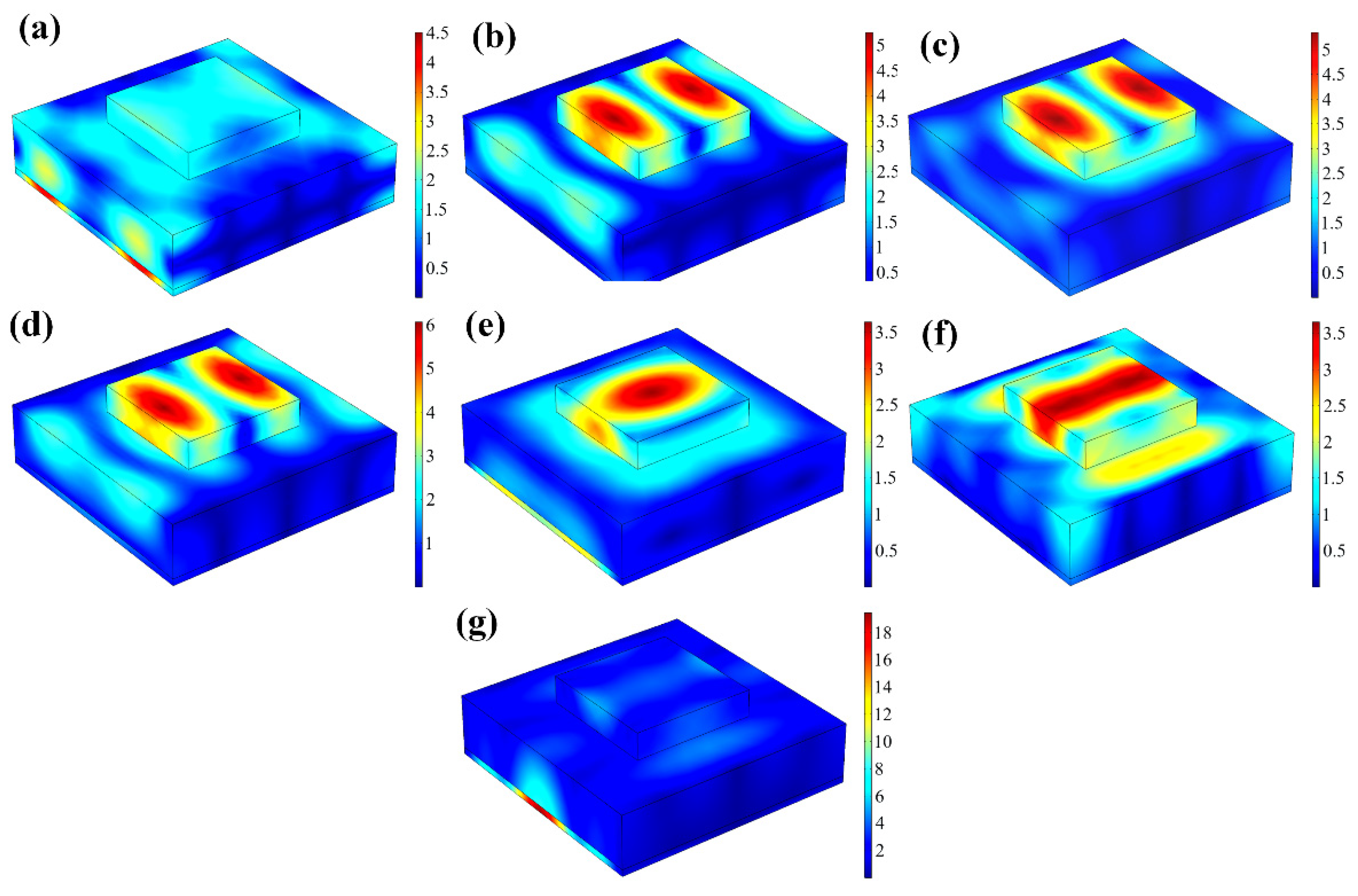
3. Results and Discussion

The main motive of the proposed structure is to identify the behaviour of the structure for the different refractive index values of the sensing material. The derived results of the structure can help to identify the unknown material refractive index by observing the resonating peaks over the derived frequency. A numerically investigated borophene based refractive index sensor is analysed using various physical parameters. The structure is simulated first by considering the different refractive indices placed on the top of the Ag resonator. The effect of variation in absorption for the different refractive indices is shown in Figure 2.
Similarly, the reflectance values for the overall structure regarding frequency and refractive index are shown in Figure 3. The size of the resonator structure is the defining element for the value of resonance. The dipole moments are created over the edge of both materials, where the light interacts with the Ag resonator and borophene. The refractive index of the top material makes overall changes in the effective refractive index of the overall structure, which results in different resonating peaks. We can observe from Figure 2 and Figure 3 that the resonating peaks are different for the different refractive index values of the sensing structure.
Figure 4 shows the variation in absorption for the different sizes of the silver patch. The silver structure is designed as a squared patch geometry. The variation in the peak resonance is relatively similar for the lower frequency than 200 THz. The sudden change is observed after 200 THz because of the destructive resonance effect. Lower values of the Rg make resonance for the higher frequency (>200 THz), while the larger values of the Rg make the perfect absorption for the lower frequency (<200 THz) spectrum. Similarly, We have also identified the effect on absorption for the different values of this patch size. The results of the absorption are shown in Figure 5. the effect of the borophene squared patch dimension Bg on the absorption spectrum is shown in Figure 5.
We can observe that the absorption peaks’ amplitude remains constant for the specific resonating frequency. At the point of 200 THz, the Ag patch makes perfect absorption, and it constructs a strong electric field across the edge, which reduces the resonating amplitude across the borophene sheet. It can be related that the absorption remains constant for the different values of the Bg while the peak of resonance changes for different values of Rg. The effect of the silica height on absorption values is presented in Figure 6. The resonance shift depends on the height of the silica layer, as observed in Figure 6. This resonance shift is highly sensitive to frequency values and silica substrate height. The effect of the oblique angle incident on absorption is calculated (0° to 80°), and the response is presented in Figure 7. It is identified that for the higher values of the frequency (>200 THz), the oblique angle incident does not affect the absorption and makes structure polarization insensitive. On the lower side of the frequency (<200 THz), a resonating point near 190 THz shows the absorption polarization-insensitive up to the input incident angle of 40°. Similarly, a resonating point near 200 THz makes the system stable for the wave incident range of 20° to 80°.
The sensitivity of the proposed structure is calculated using the equation of Δ S = Δ ƒ / Δ n , which is measured in terms of THz (Terahertz)/RIU (Refractive index Unit) [45]. In this formula, Δ ƒ is the difference between two consecutive frequency peaks, and Δ n is the difference between respective refractive index points. We have first calculated the peak resonance frequency points for the different refractive indices of the analyte. In the next step, we have plotted the variation in the resonance frequency for the different refractive index values of the analyte. The calculated sensitivity variation following the peak resonance points is shown in Figure 8. The numbers denoted in Figure 8 shows the sensitivity values between two consecutive points. A similar type of point can also be observed in Figure 2. The maximum and minimum sensitivity variations are 660 THz/RIU and 40 THz/RIU. This structure provides the fundamental idea for selecting the layer for the borophene based sensor design structure and its feasibilities with other materials.
The proposed results can be applied to identify the effect of the different biomaterials on the overall absorption structure. In addition, the presented results can also help identify the unknown refractive index of the material, which was the primary requirement for the biosensing application.
Figure 9 shows the variation in the electric field intensity for the different values of refractive index and resonating frequency. Similarly, Figure 10 shows the normalized electric field intensity E (V/m) variation for the resonating peaks by making the analyte refractive index 1.1. It is observed that the resonance depends on the ditablepole moments generation. Moreover, a multilayered structure is responsible for generating signal trapping. In Figure 9, it is observed that the resonance peaks are generated because of the higher electric field concentration over the Ag resonator or borophene patch layer. The figure of Merit (FOM) of the proposed structure is calculated using FOM = Sensitivity/FWHM [46]. The calculated FOM response for the different analyte materials is shown in Figure 11. The maximum FOM of 444 RIU−1 is observed in the FOM-1 response. Table 1 shows the variation in sensitivity in THz/TIU and nm/RIU units. It is observed that the maximum sensitivity variation of the overall structure is 660 THz/RIU and 4471 nm/RIU. Table 2 compares the proposed sensor with published structure type, FOM, and operating wavelength results. It is identified that the borophene based refractive index sensor is offered the FOM = 444 RIU−1 and sensitivity = 4471 nm/RIU (660 THz/RIU).

4. Conclusions

The borophene-based refractive index sensor for the infrared frequency spectrum is numerically investigated. The results are presented in the proposed manuscript. The structure is investigated over the 180 THz to 250 THz frequency range. This manuscript has designed a single layered borophene structure with Ag as substrate. The borophene on the Ag substrate is covered with the silica layer to prevent borophene from oxidation. The squared patched resonator of Ag is placed on the top of the silica to generate the resonating frequency. The behaviour of the structure is identified in terms of mainly absorption and reflectance. The proposed manuscript also investigates the other physical parameters, resonator height, silica height, oblique angle incident, and sensitivity variation. This structure provides wide-angle stability of 0° to 80° of operation for the wide frequency (239 to 245 THz and 207 to 209 THz). The maximum and minimum sensitivity variations are 660 THz/RIU and 40 THz/RIU. With these achieved results of absorption and sensitivity of the proposed structure, it can be used for label-free biosensing applications and various THz photonics and biomedical applications.

Author Contributions

Conceptualization, V.S. and A.G.A.; methodology, V.S. and A.G.A.; software, V.S.; validation, V.S. and A.G.A.; formal analysis, V.S. and A.G.A.; investigation, S.L., V.S. and A.G.A.; writing—original draft preparation, S.L., V.S. and A.G.A.; writing—review and editing, V.S. and A.G.A.; visualization, V.S.; supervision, V.S. and A.G.A.; project administration, V.S. and A.G.A.; funding acquisition, A.G.A. All authors have read and agreed to the published version of the manuscript.

Funding

This research received no external funding.

Institutional Review Board Statement

Not applicable.

Informed Consent Statement

Not applicable.

Data Availability Statement

Not applicable.

Conflicts of Interest

The authors declare no conflict of interest.

References

  1. Ferrari, A.C.; Bonaccorso, F.; Fal’ko, V.; Novoselov, K.S.; Roche, S.; Bøggild, P.; Borini, S.; Koppens, F.H.L.; Palermo, V.; Pugno, N.; et al. Science and Technology Roadmap for Graphene, Related Two-Dimensional Crystals, and Hybrid Systems. Nanoscale 2015, 7, 4598–4810. [Google Scholar] [CrossRef] [PubMed] [Green Version]
  2. Novoselov, K.S.; Fal’Ko, V.I.; Colombo, L.; Gellert, P.R.; Schwab, M.G.; Kim, K. A Roadmap for Graphene. Nature 2012, 490, 192–200. [Google Scholar] [CrossRef] [PubMed]
  3. Klinovaja, J.; Loss, D. Spintronics in MoS2 Monolayer Quantum Wires. Phys. Rev. B-Condens. Matter Mater. Phys. 2013, 88, 075404. [Google Scholar] [CrossRef] [Green Version]
  4. Xu, Y.; Gan, Z.; Zhang, S.C. Enhanced Thermoelectric Performance and Anomalous Seebeck Effects in Topological Insulators. Phys. Rev. Lett. 2014, 112, 226801. [Google Scholar] [CrossRef] [PubMed] [Green Version]
  5. Mannix, A.J.; Zhou, X.F.; Kiraly, B.; Wood, J.D.; Alducin, D.; Myers, B.D.; Liu, X.; Fisher, B.L.; Santiago, U.; Guest, J.R.; et al. Synthesis of Borophenes: Anisotropic, Two-Dimensional Boron Polymorphs. Science 2015, 350, 1513–1516. [Google Scholar] [CrossRef] [PubMed] [Green Version]
  6. Geim, A.K.; Novoselov, K.S. The Rise of Graphene. In Nanoscience and Technology: A Collection of Reviews from Nature Journals; World Scientific Publishing Co.: Singapore, 2009; pp. 11–19. ISBN 9789814287005. [Google Scholar]
  7. Arora, R.B.; Madan, B.R.; Pathak, R.K. Antiarrhythmics. VIII. Chloroquine, Amodiaquine, Procaine Amide and Quinidine in Experimental Auricular Arrhythmias Simulating Clinical Disorders. Indian J. Med. Res. 1956, 44, 453–462. [Google Scholar] [CrossRef] [Green Version]
  8. Eigler, S. A New Parameter Based on Graphene for Characterizing Transparent, Conductive Materials. Carbon N. Y. 2009, 47, 2936–2939. [Google Scholar] [CrossRef]
  9. Ponraj, J.S.; Xu, Z.Q.; Dhanabalan, S.C.; Mu, H.; Wang, Y.; Yuan, J.; Li, P.; Thakur, S.; Ashrafi, M.; McCoubrey, K.; et al. Photonics and Optoelectronics of Two-Dimensional Materials beyond Graphene. Nanotechnology 2016, 27, 462001. [Google Scholar] [CrossRef]
  10. Rakhshani, M.R. Wide-Angle Perfect Absorber Using a 3D Nanorod Metasurface as a Plasmonic Sensor for Detecting Cancerous Cells and Its Tuning with a Graphene Layer. Photonics Nanostruct. Fundam. Appl. 2021, 43, 100883. [Google Scholar] [CrossRef]
  11. Wang, J. Two-Dimensional Semiconductors for Ultrafast Photonic Applications. In Optical Components and Materials XII; Jiang, S., Digonnet, M.J.F., Eds.; SPIE: Bellingham, WA, USA, 2015; Volume 9359, p. 935902. [Google Scholar]
  12. Luo, A.-P.; Liu, M.; Wang, X.-D.; Ning, Q.-Y.; Xu, W.-C.; Luo, Z.-C. Few-Layer MoS2-Deposited Microfiber as Highly Nonlinear Photonic Device for Pulse Shaping in a Fiber Laser [Invited]. Photonics Res. 2015, 3, A69. [Google Scholar] [CrossRef]
  13. Li, L.; Yu, Y.; Ye, G.J.; Ge, Q.; Ou, X.; Wu, H.; Feng, D.; Chen, X.H.; Zhang, Y. Black Phosphorus Field-Effect Transistors. Nat. Nanotechnol. 2014, 9, 372–377. [Google Scholar] [CrossRef] [PubMed] [Green Version]
  14. Mak, K.F.; Lee, C.; Hone, J.; Shan, J.; Heinz, T.F. Atomically Thin MoS2: A New Direct-Gap Semiconductor. Phys. Rev. Lett. 2010, 105, 136805. [Google Scholar] [CrossRef] [PubMed] [Green Version]
  15. Lei, Z.; Guo, B. 2D Material-Based Optical Biosensor: Status and Prospect. Adv. Sci. 2022, 9, 2102924. [Google Scholar] [CrossRef] [PubMed]
  16. Xie, Z.; Meng, X.; Li, X.; Liang, W.; Huang, W.; Chen, K.; Chen, J.; Xing, C.; Qiu, M.; Zhang, B.; et al. Two-Dimensional Borophene: Properties, Fabrication, and Promising Applications. Research 2020, 2020, 2624617. [Google Scholar] [CrossRef]
  17. Meng, F.; Chen, X.; Sun, S.; He, J. Electronic and Magnetic Properties of Pristine and Hydrogenated Borophene Nanoribbons. Phys. E Low-Dimens. Syst. Nanostructures 2017, 91, 106–112. [Google Scholar] [CrossRef] [Green Version]
  18. Moradiani, F.; Farmani, A.; Mozaffari, M.H.; Seifouri, M.; Abedi, K. Systematic Engineering of a Nanostructure Plasmonic Sensing Platform for Ultrasensitive Biomaterial Detection. Opt. Commun. 2020, 474, 126178. [Google Scholar] [CrossRef]
  19. Baetens, R.; Jelle, B.P.; Gustavsen, A. Properties, Requirements and Possibilities of Smart Windows for Dynamic Daylight and Solar Energy Control in Buildings: A State-of-the-Art Review. Sol. Energy Mater. Sol. Cells 2010, 94, 87–105. [Google Scholar] [CrossRef] [Green Version]
  20. Zhang, L.; Zhou, Y.; Guo, L.; Zhao, W.; Barnes, A.; Zhang, H.T.; Eaton, C.; Zheng, Y.; Brahlek, M.; Haneef, H.F.; et al. Correlated Metals as Transparent Conductors. Nat. Mater. 2016, 15, 204–210. [Google Scholar] [CrossRef]
  21. Rakhshani, M.R.; Rashki, M. Metamaterial Perfect Absorber Using Elliptical Nanoparticles in Multilayer Metasurface Structure with Polarization Independence. Opt. Express 2022, 30, 10387. [Google Scholar] [CrossRef]
  22. Rakhshani, M.R. Tunable and Sensitive Refractive Index Sensors by Plasmonic Absorbers with Circular Arrays of Nanorods and Nanotubes for Detecting Cancerous Cells. Plasmonics 2020, 15, 2071–2080. [Google Scholar] [CrossRef]
  23. Amoosoltani, N.; Mehrabi, K.; Zarifkar, A.; Farmani, A.; Yasrebi, N. Double-Ring Resonator Plasmonic Refractive Index Sensor Utilizing Dual-Band Unidirectional Reflectionless Propagation Effect. Plasmonics 2021, 16, 1277–1285. [Google Scholar] [CrossRef]
  24. Hamouleh-Alipour, A.; Mir, A.; Farmani, A. Design and Analytical Evaluation of a High Resistance Sensitivity Bolometer Sensor Based on Plasmonic Metasurface Structure. IEEE J. Sel. Top. Quantum Electron. 2022, 28, 1–7. [Google Scholar] [CrossRef]
  25. Rakhshani, M.R. Three-Dimensional Polarization-Insensitive Perfect Absorber Using Nanorods Array for Sensing and Imaging. IEEE Sens. J. 2020, 20, 14166–14172. [Google Scholar] [CrossRef]
  26. Rakhshani, M.R. Refractive Index Sensor Based on Dual Side-Coupled Rectangular Resonators and Nanorods Array for Medical Applications. Opt. Quantum Electron. 2021, 53, 232. [Google Scholar] [CrossRef]
  27. Rakhshani, M.R. Narrowband Plasmonic Absorber Using Gold Nanoparticle Arrays for Refractive Index Sensing. IEEE Sens. J. 2022, 22, 4043–4050. [Google Scholar] [CrossRef]
  28. Rashid, K.S.; Tathfif, I.; Yaseer, A.A.; Hassan, M.F.; Sagor, R.H. Cog-Shaped Refractive Index Sensor Embedded with Gold Nanorods for Temperature Sensing of Multiple Analytes. Opt. Express 2021, 29, 37541. [Google Scholar] [CrossRef]
  29. Rakhshani, M.R.; Mansouri-Birjandi, M.A. High Sensitivity Plasmonic Refractive Index Sensing and Its Application for Human Blood Group Identification. Sens. Actuators B Chem. 2017, 249, 168–176. [Google Scholar] [CrossRef]
  30. Rakhshani, M.R.; Mansouri-Birjandi, M.A. A High-Sensitivity Sensor Based on Three-Dimensional Metal–Insulator–Metal Racetrack Resonator and Application for Hemoglobin Detection. Photonics Nanostruct.-Fundam. Appl. 2018, 32, 28–34. [Google Scholar] [CrossRef]
  31. Hassan, M.F.; Tathfif, I.; Radoan, M.; Sagor, R.H. A Concentric Double-Ring Resonator Based Plasmonic Refractive Index Sensor with Glucose Sensing Capability. In Proceedings of the IEEE Region 10 Annual International Conference, Osaka, Japan, 16–19 November 2020; Volume 2020, pp. 91–96. [Google Scholar]
  32. Rashid, K.S.; Hassan, M.F.; Yaseer, A.A.; Tathfif, I.; Sagor, R.H. Gas-Sensing and Label-Free Detection of Biomaterials Employing Multiple Rings Structured Plasmonic Nanosensor. Sens. Bio-Sens. Res. 2021, 33, 100440. [Google Scholar] [CrossRef]
  33. Giovannetti, G.; Khomyakov, P.A.; Brocks, G.; Karpan, V.M.; Van Den Brink, J.; Kelly, P.J. Doping Graphene with Metal Contacts. Phys. Rev. Lett. 2008, 101, 026803. [Google Scholar] [CrossRef]
  34. Feng, B.; Sugino, O.; Liu, R.Y.; Zhang, J.; Yukawa, R.; Kawamura, M.; Iimori, T.; Kim, H.; Hasegawa, Y.; Li, H.; et al. Dirac Fermions in Borophene. Phys. Rev. Lett. 2017, 118, 096401. [Google Scholar] [CrossRef] [PubMed] [Green Version]
  35. Massote, D.V.P.; Liang, L.; Kharche, N.; Meunier, V. Electronic, Vibrational, Raman, and Scanning Tunneling Microscopy Signatures of Two-Dimensional Boron Nanomaterials. Phys. Rev. B 2016, 94, 195416. [Google Scholar] [CrossRef] [Green Version]
  36. Tsafack, T.; Yakobson, B.I. Thermomechanical Analysis of Two-Dimensional Boron Monolayers. Phys. Rev. B 2016, 93, 165434. [Google Scholar] [CrossRef] [Green Version]
  37. Sun, H.; Li, Q.; Wan, X.G. First-Principles Study of Thermal Properties of Borophene. Phys. Chem. Chem. Phys. 2016, 18, 14927–14932. [Google Scholar] [CrossRef]
  38. Peng, B.; Zhang, H.; Shao, H.; Xu, Y.; Zhang, R.; Zhu, H. The Electronic, Optical, and Thermodynamic Properties of Borophene from First-Principles Calculations. J. Mater. Chem. C 2016, 4, 3592–3598. [Google Scholar] [CrossRef] [Green Version]
  39. Kondo, T. Recent Progress in Boron Nanomaterials. Sci. Technol. Adv. Mater. 2017, 18, 780–804. [Google Scholar] [CrossRef] [Green Version]
  40. Li, D.; Gao, J.; Cheng, P.; He, J.; Yin, Y.; Hu, Y.; Chen, L.; Cheng, Y.; Zhao, J. 2D Boron Sheets: Structure, Growth, and Electronic and Thermal Transport Properties. Adv. Funct. Mater. 2020, 30, 1904349. [Google Scholar] [CrossRef]
  41. Bezugly, V.; Kunstmann, J.; Grundkötter-Stock, B.; Frauenheim, T.; Niehaus, T.; Cuniberti, G. Highly Conductive Boron Nanotubes: Transport Properties, Work Functions, and Structural Stabilities. ACS Nano 2011, 5, 4997–5005. [Google Scholar] [CrossRef]
  42. Zhang, Z.; Penev, E.S.; Yakobson, B.I. Two-Dimensional Boron: Structures, Properties and Applications. Chem. Soc. Rev. 2017, 46, 6746–6763. [Google Scholar] [CrossRef]
  43. Johnson, P.B.; Christy, R.W. Optical Constants of the Noble Metals. Phys. Rev. B 1972, 6, 4370–4379. [Google Scholar] [CrossRef]
  44. Tathfif, I.; Yaseer, A.A.; Rashid, K.S.; Sagor, R.H. Metal-Insulator-Metal Waveguide-Based Optical Pressure Sensor Embedded with Arrays of Silver Nanorods. Opt. Express 2021, 29, 32365. [Google Scholar] [CrossRef] [PubMed]
  45. Tathfif, I.; Rashid, K.S.; Yaseer, A.A.; Sagor, R.H. Alternative Material Titanium Nitride Based Refractive Index Sensor Embedded with Defects: An Emerging Solution in Sensing Arena. Results Phys. 2021, 29, 104795. [Google Scholar] [CrossRef]
  46. Xu, Y.; Wu, L.; Ang, L.K. Surface Exciton Polaritons: A Promising Mechanism for Refractive-Index Sensing. Phys. Rev. Appl. 2019, 12, 024029. [Google Scholar] [CrossRef] [Green Version]
  47. Shih, W.-C.; Santos, G.M.; Zhao, F.; Zenasni, O.; Arnob, M.M.P. Simultaneous Chemical and Refractive Index Sensing in the 1–2.5 Μm Near-Infrared Wavelength Range on Nanoporous Gold Disks. Nano Lett. 2016, 16, 4641–4647. [Google Scholar] [CrossRef]
  48. Pinapati, P.; Cherukulappurath, S. Hybrid Dielectric-Plasmonic Nanocomposite Arrays for Bulk and Local Refractive Index Sensing. Plasmonics 2020, 15, 441–447. [Google Scholar] [CrossRef]
  49. Stakenborg, T.; Lagae, L. Gold Nanoring as a Sensitive Plasmonic Biosensor for On-Chip DNA Detection. Appl. Phys. Lett. 2012, 100, 173114. [Google Scholar] [CrossRef] [Green Version]
  50. Lodewijks, K.; Van Roy, W.; Borghs, G.; Lagae, L.; Van Dorpe, P. Boosting the Figure-Of-Merit of LSPR-Based Refractive Index Sensing by Phase-Sensitive Measurements. Nano Lett. 2012, 12, 1655–1659. [Google Scholar] [CrossRef] [Green Version]
  51. Chen, H.; Kou, X.; Yang, Z.; Ni, W.; Wang, J. Shape- and Size-Dependent Refractive Index Sensitivity of Gold Nanoparticles. Langmuir 2008, 24, 5233–5237. [Google Scholar] [CrossRef]
  52. Pryce, I.M.; Kelaita, Y.A.; Aydin, K.; Atwater, H.A. Compliant Metamaterials for Resonantly Enhanced Infrared Absorption Spectroscopy and Refractive Index Sensing. ACS Nano 2011, 5, 8167–8174. [Google Scholar] [CrossRef]
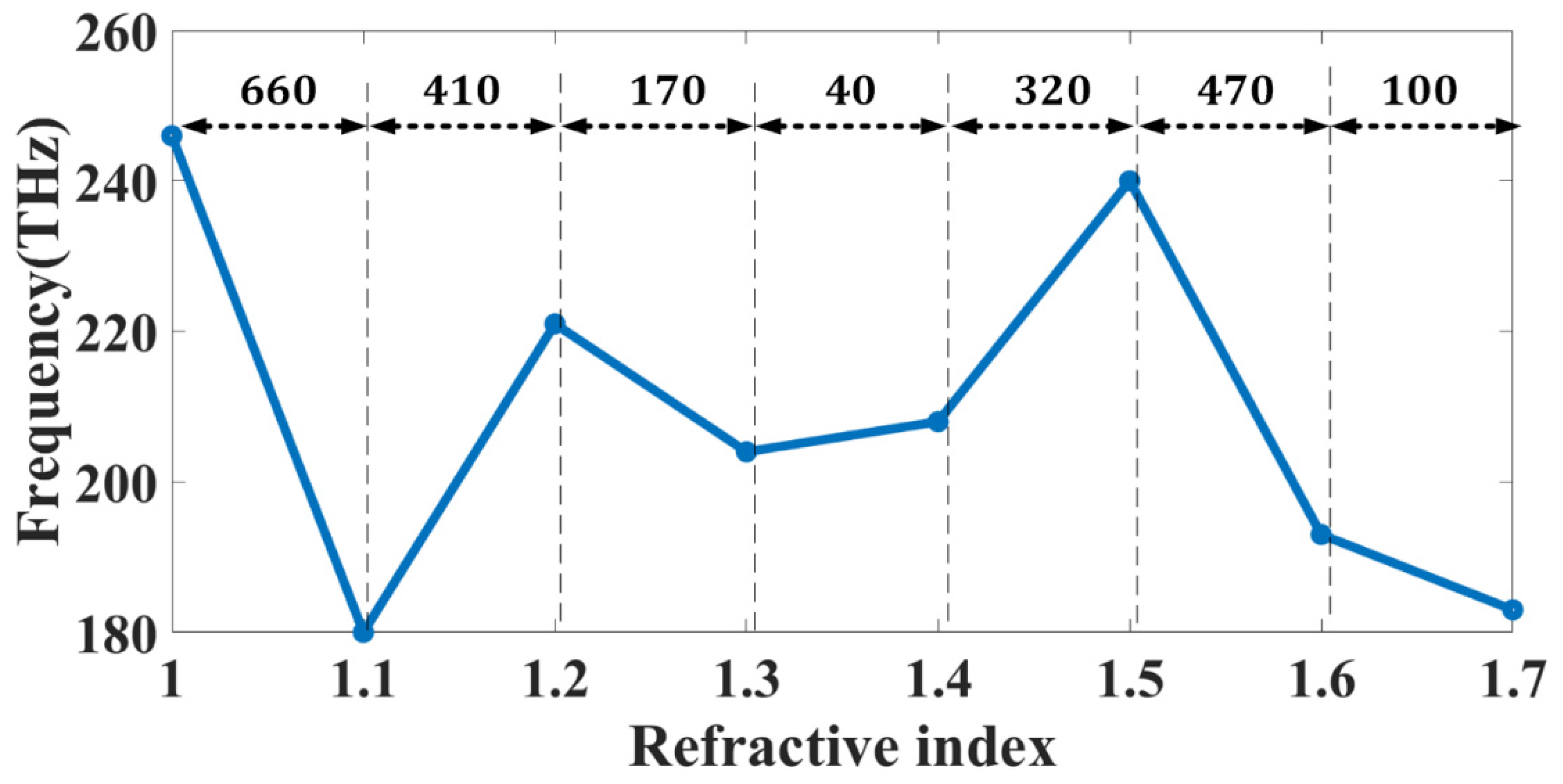
Figure 1. Schematic of the borophene based refractive index sensor. (a) Three-dimensional view with the stacked structure Silver-Borophene-Silica-Silver-analyte/sensing medium. (b) side view of the proposed structure.
Photonics 09 00279 g001
Figure 2. Variation in the absorption for the different refractive index values.
Photonics 09 00279 g002
Figure 3. Variation in the reflectance for the different refractive index values.
Photonics 09 00279 g003
Figure 4. Calculated absorption response for the different size values of the squared silver resonator.
Photonics 09 00279 g004
Figure 5. Calculated absorption response for the different size values of the borophene squared patch.
Photonics 09 00279 g005
Figure 6. Variation in absorption peaks for the different values of the silica thickness.
Photonics 09 00279 g006
Figure 7. Effect of the oblique angle on the incident on the absorption values. The oblique angle varies from 0° to 80°.
Photonics 09 00279 g007
Figure 8. Variation in the peak resonance frequency for the different values of the refractive index of sample material.
Photonics 09 00279 g008
Figure 9. Variation electric field intensity for the different values of the refractive index of sample analyte material and incident frequency. Normalized electric field intensity E (V/m) for (a) n = 1.1, ω = 180 THz, (b) n = 1.2, ω = 221 THz, (c) n = 1.3, ω = 204 THz, (d) n = 1.4, ω = 208 THz, (e) n = 1.5, ω = 240 THz, (f) n = 1.6, ω = 193 THz, (g) n = 1.7, ω = 183 THz.
Photonics 09 00279 g009
Figure 10. Variation in the electric filed distribution E (V/m) for peak resonance frequency values. Electric field distribution at (a) 191 THz, (b) 199.4 THz, (c) 209.8 THz, (d) 220.5 THz, (e) 233.4 THz, and (f) 236 THz. The refractive index of the analyte is considered 1.1 for this result.
Photonics 09 00279 g010
Figure 11. Calculated FOM at the different frequencies for the different refractive indices of an analyte.
Photonics 09 00279 g011
Table 1. Peak resonating frequency and its respective sensitivity values.
Refractive IndexPeak Resonating Frequency
(in THz)
Equivalent Wavelength
(in µm)
Sensitivity
(THz/RIU)
Sensitivity
(nm/RIU)
12461.21956604471
1.11801.66664103092
1.22211.35741701131
1.32041.470540282
1.42081.44233201923
1.52401.25004703044
1.61931.5544100849
1.71831.6393--
Table 2. Comparison of the proposed structure with the already existing structure.
Structure TypeFOM (RIU−1)Wavelength (nm)Sensitivity (nm/RIU)Reference
Discs-1000~2500525.7[47]
Nanocomposite arrays10500~900300[48]
Nanorings3.1798350[49]
Nanorings16.5980380[50]
Nanoparticles0.652744[51]
Split-ring resonators8.514201192[52]
Nanorods and nanotube arrays19.5500~25001055[22]
Rectangular Array4441200~1600
(180–250 THz)
4471Our Work
Publisher’s Note: MDPI stays neutral with regard to jurisdictional claims in published maps and institutional affiliations.

