Abstract
The scattering-type scanning near-field optical microscope (s-SNOM) has become a powerful imaging and nano-spectroscopy tool, which is widely used in the characterization of electronic and photonic devices, two-dimensional materials and biomolecules. However, in the published literature, nano-spectroscopy is mainly employed in the mid-infrared band, and the near-infrared (NIR) nano-spectroscopy with broadband spectral range has not been well discussed. In the present paper, we introduce a home-built near-field NIR spectroscopy and imaging set-up that is based on a laser-driven light source (LDLS). By mapping the Ge-Au periodic grating sample and the photonic topology device, a ~30 nm spatial resolution and the excellent capability of characterizing complex samples are demonstrated. Spectra obtained by experiment reveal the optical band-gap of Ge with a spectral resolution of 25 cm−1, and a spectral range from 900 to 2000 nm. This technology is expected to provide a novel and unique approach for near-field NIR spectroscopy and imaging.
1. Introduction
Conventional optical microscopy and micro-spectroscopy are based on the principle of optical imaging; according to the Abbe diffraction limit theorem, the best spatial resolution of conventional optical microscopy and micro-spectroscopy is about half of the light wavelength. This obviously cannot meet the growing demand for exploring the nano world. s-SNOM, which emerged at the end of the last century [1], has overcome the constraints of the diffraction limit. Its spatial resolution can reach ~10 nm, which depends on the sharpness of the AFM probe tip and has nothing to do with the light wavelength [2,3]. To date, s-SNOM has been widely used in photonic and electronic devices [4,5], polymers [3], 2D materials [6,7] and biological [8] research.
The material composition and nanoscale structure are crucial attributes of nanomaterial characteristics. Although s-SNOM has demonstrated strong capabilities in nanoscale optical imaging, in many more in-depth studies, the combination of absorption spectroscopy and s-SNOM (usually named near-field spectroscopy or nano-spectroscopy in the reported literature) can further provide more physical properties and chemical information of the samples [9]. In the past ten years, this growing demand for nano-spatial resolution spectral characterization has prompted the rapid development of Fourier transform infrared nano-spectroscopy (nano-FTIR), which combines s-SNOM and Fourier transform infrared spectroscopy (FTIR). With the progress of s-SNOM and the use of various advanced broadband light sources, such as the difference frequency generation source (DFG) [10], synchrotron radiation light source (SRLS) [11,12] and plasma light source (PLS) [13,14], nano-FTIR has shown great potential in the research fields of semiconductor devices [4,12], two-dimensional materials [15,16], biology [11,17,18,19] and polymers [20]. As far as we know, much work has focused on the mid-infrared band near-field spectroscopy, however, there are only a few published works exploring those applications in the NIR band [21,22]. In many research fields, such as photonic topological devices [23], plasmonic nanostructures [21,24] and two-dimensional materials [25,26,27,28], researchers also have a huge demand for NIR nano-spectroscopy, and this is worthy of further exploration.
In this work, we introduce the basic working principles and characteristics of LDLS, which can cover the entire NIR band and have greater brightness. Subsequently, we describe our home-built near-field imaging and spectroscopy set-up based on this light source. In order to demonstrate the stability and the spatial resolution of the home-built set-up, we use this set-up to perform near-field optical imaging of a Ge-Au periodic grating sample and a photonic topology device. Finally, we obtain the near-field absorption spectrum of Ge with reference to Au, and compare it with the spectrum predicted by the point dipole model (PDM) [29] using known literature values for the dielectric functions of Ge [30].
2. Experimental Set-Up
2.1. Laser-Driven Light Source
The light source used in our set-up was a laser driven plasma light source (EQ77, Energetiq), and its working principle is shown in Figure 1a. Focusing the laser beam (emitted by a 50 W near-infrared diode laser) into a chamber filled with noble gas xenon (gas pressure about 30 bar), the plasma, after ignition by an electrical discharge between the two electrodes (the power of the discharge electrode is ~40 W), was maintained by the diode laser. As free electrons decelerate due to the interaction with ions, atoms and other electrons, the noble gas plasma emits a continuous spectrum (due to the cut-off of the quartz bulb, the spectrum only covers the ultraviolet to near-infrared band). Figure 1b shows the comparison of the spectral range and spectral radiance of LDLS, tungsten halogen source, xenon light source and deuterium light source commonly used in VIS-NIR spectroscopy; the data is obtained from [31]. It is noteworthy that LDLS can also be used as a black body radiation source for mid-infrared spectroscopy by using mid-infrared-transmitting light windows (KBr or ZnSe) [14,32,33]. Benefiting from the small focused beam spot size with only several microns, the plasma of the LDPS is confined to a volume of an estimated 125 µm × 320 µm tiny ellipsoid. For comparison, the filament length of tungsten halogen lamp is about several millimeters, and the estimated plasma volume of the recently reported plasma source based on a discharge arc [13] is 4–20 times larger than the one from the LDLS. The smaller light emission volume of LDLS means that the emitted light has the higher spatial coherence and.and the illuminating light can be more effectively focused to the ~15 um long AFM tip, which acts as an optical antenna to concentrate light to the tip apex. Note that LDLS also has an affordable cost (compared to the femtosecond laser source [21]) and a very compact structure; it is installed in a 5 × 13 × 25 cm aluminum chamber with a quartz window, which is very suitable for use as a table-top light source.
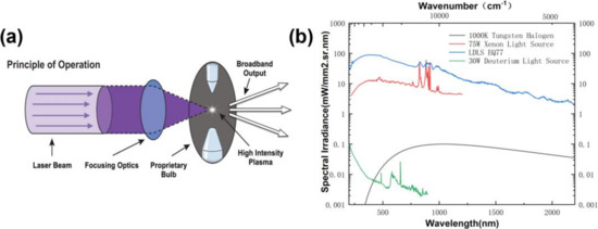
Figure 1.
Laser-driven light source. (a) The working principle and structure of the LDLS, and (b) comparison of the spectral range and spectral irradiance of common light sources in VIS−NIR spectroscopy [30].
2.2. Home-Built Set-Up and Working Mechanism
The schematic diagram of our home-built set-up is shown in Figure 2. It is mainly composed of an LDLS, a Michelson interferometer (FTIR), a modified atomic force microscope (AFM) and a signal processing system. The light emitted by the LDLS is collimated by the first off-axis parabolic mirror (OAP) (f = 50.8 mm, NA = 0.375). In order to filter out the unwanted stray light and improve the spatial coherence, the beam was focused by the second OAP through a 30 μm diameter pinhole for spatial filtering, and then collimated again by the third OAP. The beam power passing through the pinhole was measured to be ~17.8 mW (PM100D, Thorlabs, North Newton, USA). Subsequently, the collimated beam was focused by the fourth OAP (f = 25.4 mm, NA = 0.5) onto a commercial dynamic mode metallic AFM probe tip (Arrow NCPt, NanoWorld, Neuchatel, Switzerland). As a result, the interaction between the tip, light and sample induces scattered light that contains the spectral characteristics of the sample. Then, this scattering light was collected by an OAP and sent to FTIR, finally detected by the detector (PDA10D, Thorlabs).
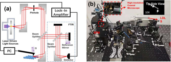
Figure 2.
Home-built near-field spectroscopy and imaging set-up with a laser-driven light source. (a) Schematic of the set-up, and (b) physical image of our home-built set-up.
It should be pointed out that the detector detects the sum of scattered light, although there is an obvious field enhancement in the tip-sample region; however, this region is still too small (a tip apex radius of about 10–20 nm), relative to the focal spot radius (in this set-up it is ~15 μm). The near-field scattering signals were obliterated in the useless far-field scattering signals of the sample, tip and probe cantilever. It is necessary to eliminate these far-field scattering signals when the set-up is working. Therefore, AFM adopted the tapping mode, and when the AFM probe vibrated at a frequency Ω in the z direction (the tapping frequency is ~270kHz, the amplitude is about ~60 nm), the near-field signals in the tip-sample region periodically changed with the distance of the tip-sample nonlinearly. In the signal processing system, the lock-in amplifier (HF2LI, Zurich Instrument) demodulated the detector signals at a higher harmonic frequency (nΩ, n = 2, 3, …) [9,34], then the near-field signals from the tip-sample region could be effectively extracted.
The reference mirror was controlled by a high-precision linear stage (L511, PI). On the one hand, the set-up can be used as an s-SNOM (mapping the lock-in signal of the sample) when the interference mirror is fixed at the zero path difference (ZPD) position. On the other hand, it can be used as a nano-FTIR when we acquire interferograms by collecting the lock-in signal and sweeping the linear stage (moving the reference mirror). Then, the near-field spectrum can be obtained by the Fourier transform of the interferogram.
3. Experimental Results and Analysis
3.1. Near-Field Imaging
Using the approach curve to judge the extraction effect of the near-field signal is a common method in the field of s-SNOM [2,13,35,36,37]. Figure 3 plots the approach curve on the Au surface. This approach curve is obtained by setting the reference mirror to the ZPD position and recording the 2Ω signal (lock-in amplifier demodulates with the second harmonic), as we retract the sample away from the AFM tip. The near-field signal decays exponentially with the increase in the tip-sample distance, which shows that the near-field signal can be effectively extracted when the second harmonic is used for signal demodulation.
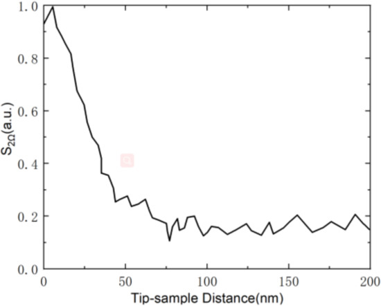
Figure 3.
Normalized approach curve obtained at the second harmonic with the reference mirror set to the ZPD position.
For demonstrating the spatial resolution, we fabricated, using the lift-off technique, a 5 mm × 5 mm Ge-Au periodic grating sample on a Ge substrate. As shown in Figure 4, the thickness of the Au film in the sample is about 20 nm, and the grating period is ~1.5 μm. Setting the reference mirror to the ZPD position, we then take an AFM topography scan across the Ge-Au region, and the second harmonic near-field optical signal is simultaneously recorded. The experimental results are shown in Figure 4, in which Figure 4a is an AFM topography imaging, and Figure 4b is the imaging of the second harmonic near-field signal. Figure 4c,d correspond to the line scanning of the white dashed lines in Figure 4a,b. Figure 4c shows a decrease (~20nm) in the topography height of the Au-Ge edge, and in Figure 4d the intensity of the near-field signal also has a sharp decrease within a scanning distance of ~30nm. These results suggest that the spatial resolution (~30 nm) of our set-up is on the order of the diameter of the AFM tip-apex and not limited by the diffraction limit of the illumination wavelength.
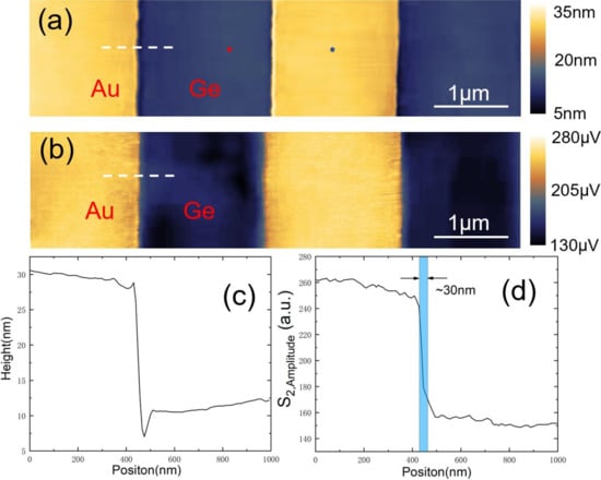
Figure 4.
(a) AFM topography (the blue and red points are the positions of the AFM probe when the spectrum was collected in Figure 6) and (b) the second harmonic near-field amplitude image obtained simultaneously on a Ge-Au periodic grating sample with the reference mirror set to the ZPD position. (c) Represents a line scanning (white dashed line) averaged over 6 consecutive horizontal lines on the topography scan, while (d) represents the same location for the near-field line scanning, and a spatial resolution of ~30 nm is demonstrated.
The topographic features of the Ge-Au grating sample are on the order of micrometers, and its AFM image is very similar to s-SNOM, which only reflects the characteristics of the material itself. As we known, the optical response of a photonic device is not only related to the material, but also closely related to the nanoscale geometry of the device. In order to demonstrate that our set-up can be used to observe the novel optical phenomena in complex photonic devices, we also performed near filed imaging of a photonic topology device, as shown in Figure 5. The device was fabricated on a silicon-on-insulator (SOI) chip, and was an equilateral triangle with a side length of 40 μm. The geometric structure and topography is shown in Figure 5a. It consists of a photonic crystal with a lattice formed by a matrix of round holes (filled with air) in high-index silicon. Figure 5b is the near-field optical imaging of this device. Photonic topology device offers novel approaches to confine and control electro-magnetic radiation at boundaries of topologically distinct materials in analogy with exotic condensed matter phenomena. In this triangular photonic topology device, electromagnetic radiation is significantly enhanced at the edges of the device, creating a phenomenon known as “boundary modes”, which form a bright stripe along the edge. References [5,38,39] present a detailed introduction to this novel and interesting phenomenon.

Figure 5.
(a) AFM topography and (b) the second harmonic near-field amplitude image obtained simultaneously on a photonic topology device with the reference mirror set to the ZPD position.
3.2. Near-Field Spectroscopy
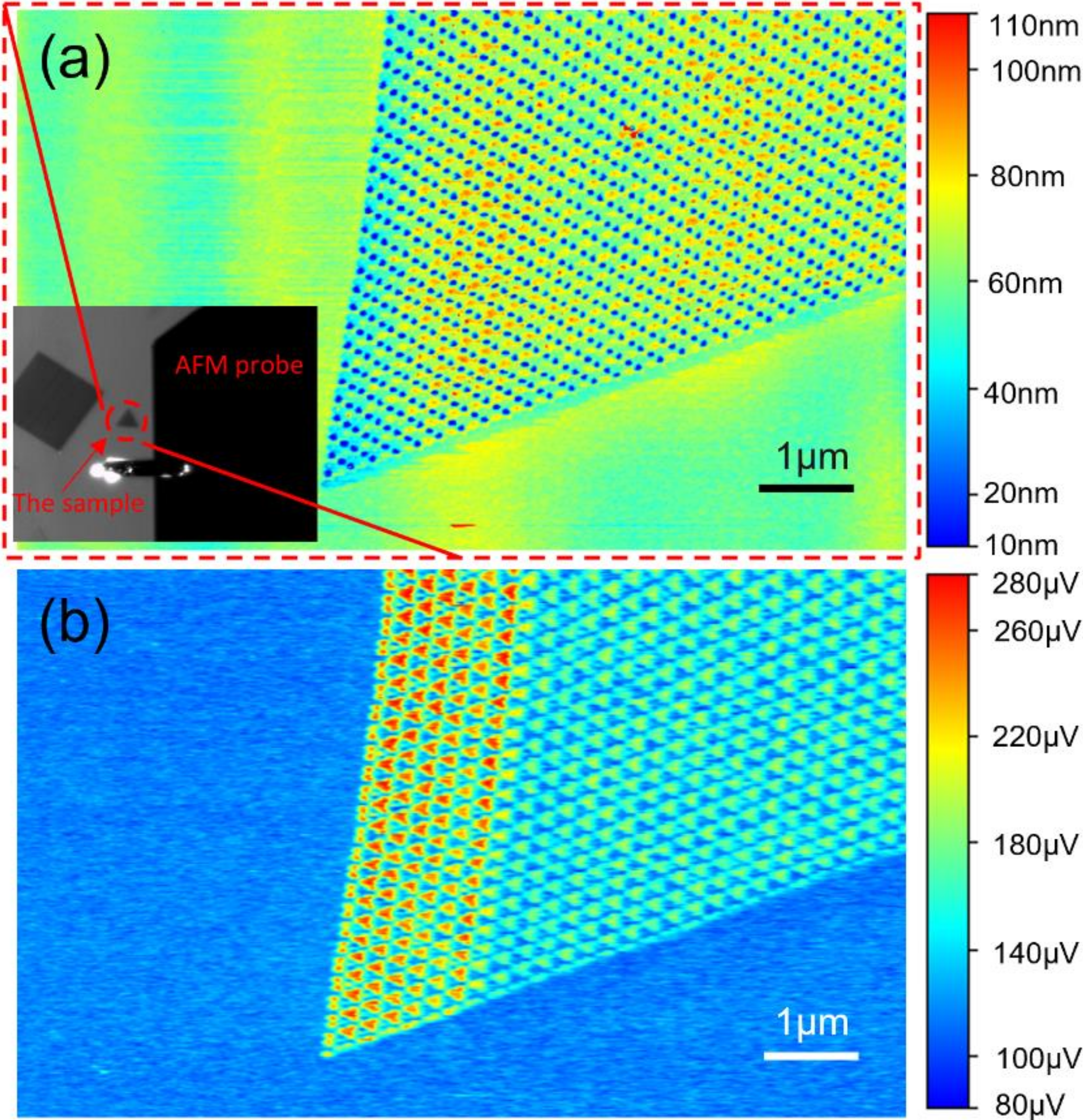
To demonstrate the LDLS capability as a broadband NIR light source for near-field spectroscopy on the Ge-Au grating sample, the AFM tip was set at points in the Au and Ge regions (corresponding to the red and blue points in Figure 4a) to collect the spectra. The reference mirror, which controlled by the high-precision linear stage, was operated in a step-scan mode, with a step size of 100 nm and step dwell time of 50 ms. The reference mirror scanned with a total distance of 200 μm, resulting in an optical path difference of 400 μm, corresponding to the spectral resolution 25 cm−1 obtained by the Fourier transform. For an acceptable signal-to-noise ratio, 6 interferograms were averaged, resulting in a total acquisition time of ~10 min per spectrum.
Figure 6a,b show the interferograms acquired with the tip on Au and Ge regions, respectively. Figure 6c shows the spectra of Au (blue line) and Ge (red line) obtained by the fast Fourier transform of the interferograms. Figure 6d presents the absorption spectrum of Ge (the red line) normalized to the Au reference spectrum ((S2,Au(v)-S2,Ge(v))/S2,Au(v)). We can observe that the absorption spectrum of Ge decays rapidly in ~1500 nm (~6700 cm−1), which corresponds to the well-known optical band gap of Ge [29]. The point dipole model is the most commonly used model in near-field spectrum prediction [9,40]; in Figure 6d, we also present the simulated spectrum (the blue line), which was calculated by the point dipole model. The spectrum obtained in the experiment had the expected semi-quantitative agreement with the spectrum simulated by PDM.
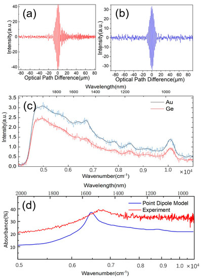
Figure 6.
(a)The interferogram of Au and (b) the interferogram of Ge. The interferograms were collected at the points when the AFM tip was set in the Au and Ge regions (corresponding to the red and blue points in Figure 4a). All of them were obtained at second harmonic demodulation. (c) The near-field spectra of Au (blue line) and Ge (red line) obtained by the fast Fourier transform of the interferograms. (d) The red line is the near-field absorption spectrum of Ge normalized to Au ((S2,Au(v)−S2,Ge(v))/S2,Au(v)), and the blue line is the spectrum predicted by the point dipole model.
4. Summary and Outlook
Exploring and developing different wavelength bands and different types of light sources is essential to the development of s-SNOM and nano-FTIR [9]. With the introduction of the LDLS, we demonstrated that it is a promising NIR light source capable of being used for near-field imaging and spectroscopy. The near-field images and spectra were obtained in our experiment demonstrate that our home-built set-up has a spatial resolution of ~30 nm and allows the optical band gap of Ge to be observed with a spectral resolution of 25 cm−1 and a spectral range from 900 to 2000 nm. With our first report on the application of LDLS to s-SNOM and nano-FTIR, considering the performance, affordable cost and compact size, we believe this approach has great potential in the nanoscale identification, quality control, and characterization of materials and devices. Further application studies and expanding the spectral to visible bands (LDLS can cover the VIS-NIR band, which is currently limited by the detector) are ongoing in our laboratory.
Author Contributions
Conceptualization, C.N. and W.Y.; methodology, C.N.; software, C.N.; investigation, C.N. and W.Y.; resources, L.T. and X.Y.; data curation, C.N. and W.Y.; writing—original draft preparation, C.N.; writing—review and editing, C.N.; supervision, L.T.; project administration, L.T.; funding acquisition, L.T. and X.Y. All authors have read and agreed to the published version of the manuscript.
Funding
This work was supported in part by the National Natural Science Foundation of China (No. 61427901); the National Key Research and Development Program of China (No. 2018YFA0704804), and the Chinese Academy of Sciences for Key Scientific Instrument and Equipment Development Project (No. YJKYYQ20180033).
Institutional Review Board Statement
Not applicable.
Informed Consent Statement
Not applicable.
Data Availability Statement
Not applicable.
Acknowledgments
The authors thank Lina Shi for providing the photonic topology device sample.
Conflicts of Interest
The authors declare no conflict of interest.
References
- Keilmann, F.; van der Weide, D.; Eickelkamp, T.; Merz, R.; Stöckle, D. Extreme sub-wavelength resolution with a scanning radio-frequency transmission microscope. Opt. Commun. 1996, 129, 15–18. [Google Scholar] [CrossRef]
- Knoll, B.; Keilmann, F. Mid-infrared scanning near-field optical microscope resolves 30 nm. J. Microsc. 1999, 194, 512–515. [Google Scholar] [CrossRef] [PubMed] [Green Version]
- Taubner, T.; Hillenbrand, R.; Keilmann, F. Nanoscale polymer recognition by spectral signature in scattering infrared near-field microscopy. Appl. Phys. Lett. 2004, 85, 5064–5066. [Google Scholar] [CrossRef]
- Huth, F.; Schnell, M.; Wittborn, J.; Ocelic, N.; Hillenbrand, R. Infrared-spectroscopic nanoimaging with a thermal source. Nat. Mater. 2011, 10, 352–356. [Google Scholar] [CrossRef] [PubMed]
- Vakulenko, A.; Kiriushechkina, S.; Wang, M.; Li, M.; Zhirihin, D.; Ni, X.; Guddala, S.; Korobkin, D.; Alù, A.; Khanikaev, A.B. Metasurfaces: Near-Field Characterization of Higher-Order Topological Photonic States at Optical Frequencies (Adv. Mater. 18/2021). Adv. Mater. 2021, 33, 2170135. [Google Scholar] [CrossRef]
- Hu, D.; Chen, K.; Chen, X.; Guo, X.; Liu, M.; Dai, Q. Tunable Modal Birefringence in a Low-Loss Van Der Waals Waveguide. Adv. Mater. 2019, 31, e1807788. [Google Scholar] [CrossRef] [PubMed]
- Hu, F.; Luan, Y.; Scott, M.E.; Yan, J.; Mandrus, D.G.; Xu, X.; Fei, Z. Imaging exciton–polariton transport in MoSe2 waveguides. Nat. Photon 2017, 11, 356–360. [Google Scholar] [CrossRef]
- Berweger, S.; Nguyen, D.M.; Muller, E.A.; Bechtel, H.A.; Perkins, T.T.; Raschke, M.B. Nano-Chemical Infrared Imaging of Membrane Proteins in Lipid Bilayers. J. Am. Chem. Soc. 2013, 135, 18292–18295. [Google Scholar] [CrossRef] [PubMed]
- Nan, C.; Yue, W.; Tao, L.; Yang, X. Fourier transform infrared nano-spectroscopy: Mechanism and applications. Appl. Spectrosc. Rev. 2021, 56, 531–552. [Google Scholar] [CrossRef]
- Gamage, S.; Howard, M.; Makita, H.; Cross, B.; Hastings, G.; Luo, M.; Abate, Y. Probing structural changes in single enveloped virus particles using nano-infrared spectroscopic imaging. PLoS ONE 2018, 13, e0199112. [Google Scholar] [CrossRef] [PubMed] [Green Version]
- Bechtel, H.A.; Muller, E.A.; Olmon, R.L.; Martin, M.C.; Raschke, M.B. Ultrabroadband infrared nanospectroscopic imaging. Proc. Natl. Acad. Sci. USA 2014, 111, 7191–7196. [Google Scholar] [CrossRef] [PubMed] [Green Version]
- Hermann, P.; Hoehl, A.; Ulrich, G.; Fleischmann, C.; Hermelink, A.; Kästner, B.; Patoka, P.; Hornemann, A.; Beckhoff, B.; Rühl, E.; et al. Characterization of semiconductor materials using synchrotron radiation-based near-field infrared microscopy and nano-FTIR spectroscopy. Opt. Express 2014, 22, 17948–17958. [Google Scholar] [CrossRef] [PubMed] [Green Version]
- Lahneman, D.J.; Huffman, T.J.; Xu, P.; Wang, S.L.; Grogan, T.; Qazilbash, M.M. Broadband near-field infrared spectroscopy with a high temperature plasma light source. Opt. Express 2017, 25, 20421–20430. [Google Scholar] [CrossRef] [PubMed]
- Wagner, M.; Jakob, D.S.; Horne, S.; Mittel, H.; Osechinskiy, S.; Phillips, C.; Walker, G.C.; Su, C.; Xu, X.G. Ultrabroadband Nanospectroscopy with a Laser-Driven Plasma Source. ACS Photon 2018, 5, 1467–1475. [Google Scholar] [CrossRef]
- Patoka, P.; Ulrich, G.; Nguyen, A.E.; Bartels, L.; Dowben, P.A.; Turkowski, V.; Rahman, T.S.; Hermann, P.; Kästner, B.; Hoehl, A.; et al. Nanoscale plasmonic phenomena in CVD-grown MoS 2 monolayer revealed by ultra-broadband synchrotron radiation based nano-FTIR spectroscopy and near-field microscopy. Opt. Express 2016, 24, 1154–1164. [Google Scholar] [CrossRef] [PubMed] [Green Version]
- Dai, S.; Fei, Z.; Ma, Q.; Rodin, A.S.; Wagner, M.; McLeod, A.S.; Liu, M.K.; Gannett, W.; Regan, W.; Watanabe, K.; et al. Tunable Phonon Polaritons in Atomically Thin van der Waals Crystals of Boron Nitride. Science 2014, 343, 1125–1129. [Google Scholar] [CrossRef] [PubMed] [Green Version]
- Kästner, B.; Johnson, C.M.; Hermann, P.; Kruskopf, M.; Pierz, K.; Hoehl, A.; Hornemann, A.; Ulrich, G.; Fehmel, J.; Patoka, P.; et al. Infrared Nanospectroscopy of Phospholipid and Surfactin Monolayer Domains. ACS Omega 2018, 3, 4141–4147. [Google Scholar] [CrossRef] [PubMed] [Green Version]
- Amenabar, I.; Poly, S.; Goikoetxea, M.; Nuansing, W.; Lasch, P.; Hillenbrand, R. Hyperspectral infrared nanoimaging of organic samples based on Fourier transform infrared nanospectroscopy. Nat. Commun. 2017, 8, 14402. [Google Scholar] [CrossRef] [PubMed] [Green Version]
- Stanic, V.; Maia, F.C.B.; Freitas, R.D.O.; Montoro, F.E.; Evans-Lutterodt, K. The chemical fingerprint of hair melanosomes by infrared nano-spectroscopy. Nanoscale 2018, 10, 14245–14253. [Google Scholar] [CrossRef] [PubMed] [Green Version]
- Meyns, M.; Primpke, S.; Gerdts, G. Library based identification and characterisation of polymers with nano-FTIR and IR-sSNOM imaging. Anal. Methods 2019, 11, 5195–5202. [Google Scholar] [CrossRef] [Green Version]
- Arieli, U.; Mrejen, M.; Suchowski, H. Broadband coherent hyperspectral near-field imaging of plasmonic nanostructures. Opt. Express 2019, 27, 9815–9820. [Google Scholar] [CrossRef] [PubMed]
- Kaltenecker, K.J.; Rao, D.S.S.; Rasmussen, M.; Lassen, H.B.; Kelleher, E.J.; Krauss, E.; Hecht, B.; Mortensen, N.A.; Grüner-Nielsen, L.; Markos, C.; et al. Near-infrared nanospectroscopy using a low-noise supercontinuum source. APL Photonics 2021, 6, 066106. [Google Scholar] [CrossRef]
- He, X.-T.; Li, M.-Y.; Qiu, H.-Y.; Ruan, W.-S.; Zhou, L.-D.; Liu, L.; Chen, X.-D.; Chen, W.-J.; Zhao, F.-L.; Dong, J.-W. In-plane excitation of a topological nanophotonic corner state at telecom wavelengths in a cross-coupled cavity. Photon Res. 2021, 9, 1423. [Google Scholar] [CrossRef]
- Zhang, S.; Li, G.-C.; Chen, Y.; Zhu, X.; Liu, S.-D.; Lei, D.Y.; Duan, H. Pronounced Fano Resonance in Single Gold Split Nanodisks with 15 nm Split Gaps for Intensive Second Harmonic Generation. ACS Nano 2016, 10, 11105–11114. [Google Scholar] [CrossRef] [PubMed]
- Eda, G.; Maier, S.A. Two-Dimensional Crystals: Managing Light for Optoelectronics. ACS Nano 2013, 7, 5660–5665. [Google Scholar] [CrossRef]
- Xu, H.; Ren, A.; Wu, J.; Wang, Z. Recent Advances in 2D MXenes for Photodetection. Adv. Funct. Mater. 2020, 30. [Google Scholar] [CrossRef]
- Yang, X.; Zhai, F.; Hu, H.; Hu, D.; Liu, R.; Zhang, S.; Sun, M.; Sun, Z.; Chen, J.; Dai, Q. Far-Field Spectroscopy and Near-Field Optical Imaging of Coupled Plasmon-Phonon Polaritons in 2D van der Waals Heterostructures. Adv. Mater. 2016, 28, 2931–2938. [Google Scholar] [CrossRef]
- Koperski, M.; Molas, M.; Arora, A.; Nogajewski, K.; Slobodeniuk, A.; Faugeras, C.; Potemski, M. Optical properties of atomically thin transition metal dichalcogenides: Observations and puzzles. Nanophotonics 2017, 6, 1289–1308. [Google Scholar] [CrossRef]
- Knoll, B.; Keilmann, F. Enhanced dielectric contrast in scattering-type scanning near-field optical microscopy. Opt. Commun. 2000, 182, 321–328. [Google Scholar] [CrossRef]
- Nunley, T.N.; Fernando, N.S.; Samarasingha, N.; Moya, J.M.; Nelson, C.M.; Medina, A.A.; Zollner, S. Optical constants of germanium and thermally grown germanium dioxide from 0.5 to 6.6 eV via a multisample ellipsometry investigation. J. Vac. Sci. Technol. B Nanotechnol. Microelectron. 2016, 34, 061205. [Google Scholar] [CrossRef]
- Zhu, H.; Blackborow, P. Understanding Radiance (Brightness), Irradiance and Radiant Flux. Available online: www.energetiq.com/technote-understanding-radiance-brightness-irradiance-radiant-flux (accessed on 24 April 2021).
- Lahneman, D.J.; Qazilbash, M.M. Hyperspectral infrared imaging of surface phonon-polaritons in SrTiO3. Phys. Rev. B 2021, 104, 235433. [Google Scholar] [CrossRef]
- McArdle, P.; Lahneman, D.J.; Biswas, A.; Keilmann, F.; Qazilbash, M.M. Near-field infrared nanospectroscopy of surface phonon-polariton resonances. Phys. Rev. Res. 2020, 2, 023272. [Google Scholar] [CrossRef]
- Nan, C.H.E.N.; Yue, W.A.N.G.; Wang, B.Y.; Yang, X.I.A.; Tao, L.I.U. Research on numerical model of nano-FTIR system based on COMSOL. Spectrosc. Spectr. Anal. 2021, 41, 1125. [Google Scholar]
- Xu, X.G.; Rang, M.; Craig, I.M.; Raschke, M.B. Pushing the Sample-Size Limit of Infrared Vibrational Nanospectroscopy: From Monolayer toward Single Molecule Sensitivity. J. Phys. Chem. Lett. 2012, 3, 1836–1841. [Google Scholar] [CrossRef] [PubMed]
- Khatib, O.; Bechtel, H.A.; Martin, M.C.; Raschke, M.B.; Carr, G.L. Far Infrared Synchrotron Near-Field Nanoimaging and Nanospectroscopy. ACS Photon 2018, 5, 2773–2779. [Google Scholar] [CrossRef]
- Autore, M.; Mester, L.; Goikoetxea, M.; Hillenbrand, R. Substrate matters: Surface-polariton enhanced infrared nanospectroscopy of molecular vibrations. Nano Lett. 2019, 19, 8066–8073. [Google Scholar] [CrossRef]
- Ozawa, T.; Price, H.M.; Amo, A.; Goldman, N.; Hafezi, M.; Lu, L.; Rechtsman, M.C.; Schuster, D.; Simon, J.; Zilberberg, O.; et al. Topological photonics. Rev. Mod. Phys. 2019, 91, 015006. [Google Scholar] [CrossRef] [Green Version]
- Arora, S.; Bauer, T.; Barczyk, R.; Verhagen, E.; Kuipers, L. Direct quantification of topological protection in symmetry-protected photonic edge states at telecom wavelengths. Light Sci. Appl. 2021, 10, 1–7. [Google Scholar] [CrossRef] [PubMed]
- Centrone, A. Infrared Imaging and Spectroscopy Beyond the Diffraction Limit. Annu. Rev. Anal. Chem. 2015, 8, 101–126. [Google Scholar] [CrossRef] [PubMed] [Green Version]


Publisher’s Note: MDPI stays neutral with regard to jurisdictional claims in published maps and institutional affiliations. |
© 2022 by the authors. Licensee MDPI, Basel, Switzerland. This article is an open access article distributed under the terms and conditions of the Creative Commons Attribution (CC BY) license (https://creativecommons.org/licenses/by/4.0/).