Communication

An All-MRR-Based Photonic Spiking Neural Network for Spike Sequence Learning

1
State Key Laboratory of Integrated Service Networks, Xidian University, Xi’an 710071, China
2
State Key Discipline Laboratory of Wide Band Gap Semiconductor Technology, School of Microelectronics, Xidian University, Xi’an 710071, China
*
Author to whom correspondence should be addressed.
Photonics 2022, 9(2), 120; https://doi.org/10.3390/photonics9020120
Submission received: 19 January 2022 / Revised: 12 February 2022 / Accepted: 15 February 2022 / Published: 20 February 2022

Abstract

:
Photonic spiking neural networks (SNN) have the advantages of high power efficiency, high bandwidth and low delay, but limitations are encountered in large-scale integration. The silicon photonics platform is a promising candidate for realizing large-scale photonic SNN because it is compatible with the current mature CMOS platforms. Here, we present an architecture of photonic SNN which consists of photonic neuron, photonic spike timing dependent plasticity (STDP) and weight configuration that are all based on silicon micro-ring resonators (MRRs), via taking advantage of the nonlinear effects in silicon. The photonic spiking neuron based on the add-drop MRR is proposed, and a system-level computational model of all-MRR-based photonic SNN is presented. The proposed architecture could exploit the properties of small area, high integration and flexible structure of MRR, but also faces challenges caused by the high sensitivity of MRR. The spike sequence learning problem is addressed based on the proposed all-MRR-based photonic SNN architecture via adopting supervised training algorithms. We show the importance of algorithms when hardware devices are limited.

1. Introduction

Neuromorphic computing has intrinsically enhanced computing power in the last decade. In particular, a spiking neural network (SNN) operates on spatiotemporal spikes as in biological neural networks, where neurons are active when stimulated with above-threshold injected pulses. Such a spike event-driven mechanism is expected to be power efficient. The computational superiority of spiking hardware has already been demonstrated [1,2,3]. However, the electronic hardware implementation of SNN suffers from energy efficiency and physical dimensions, as well as the fundamental tradeoff between bandwidth and interconnectivity. Hence, the photonic platform has become a promising candidate for neuromorphic hardware implementation due to the advantages of ultrahigh speed, high efficiency, and extremely high bandwidth.
Tremendous efforts have been devoted to the explorations of optical devices that exhibit neuron-like dynamics, biological synapse properties and algorithms [4,5,6,7,8,9,10,11,12,13,14,15,16], which are essential elements in a SNN. Existing photonic spiking neurons are mainly based on excitable semiconductor lasers [13,17,18]. One typical model of such laser neuron is vertical cavity emitting laser with saturable absorption region (VCSEL-SA), which was theoretically demonstrated to be a Leaky-Integrate and Fire neuron [17]. Based on the polarization mode competition, all-optical inhibitory dynamics were also observed in VCSEL-SA [19]. In addition, the semiconductor optical amplifiers (SOA) and the vertical-cavity SOA (VCSOA) were numerically and experimentally demonstrated to perform the spike timing dependent plasticity (STDP) function [20,21], which is a biologically observed phenomenon in synapses that related to the learning mechanism [22]. Such a STDP rule is widely employed in both supervised learning and unsupervised learning [23,24,25,26]. However, these devices are usually based on III-V platforms that are not CMOS-compatible, hence limiting the large-scale integrated applications.
Silicon-based optoelectronics is an ideal platform for photonic neural networks because it is CMOS-compatible, thereby benefits from low-cost, commercial maturity and easy integration with electronics [27,28,29,30,31,32]. A micro-ring resonator (MRR) has innate WDM compatibility and small footprints, with flexible structure and high scalability. Phase change materials (PCM) embedded on silicon waveguides were successfully used to emulate optical synapses [9,10,33]. Recently, based on nonlinear effects in silicon, a STDP scheme has been proposed via using high-order MRRs [34], in which tunable potentiation/depression windows could be generated with different time constants. Besides, due to thermo-optic and electric-optic effects in silicon, the resonance wavelength of MRR could be tuned and the transmission could be controlled [35,36,37,38,39,40], which enables MRRs as reconfigurable elements for matrix multiplication, convolutional operation [41,42], and as reconfigurable weighting in photonic computing [43,44,45]. A set of parallel-coupled MRRs, named a MRR weight bank (MRR-WB), can weight the neuron output independently over a continuous range from [–1,1] with balanced photodetectors (PDs) [43]. Due to the high sensitivity of MRR, feedback control approaches are usually adopted for weight stabilization, and the precision for continuous weight tuning has been improved to more than 8 bits in a 2-channel MRR-WB setup [44].
In addition, there are also novel photonic spiking neuron models based on passive silicon platforms, such as PCMs embedded on micro-ring [33,46] and microcavity neurons [47,48,49]. It needs to be mentioned that the former neuron utilizes PCMs to accumulate energy and switch the inner state. External incident spikes are sent to the system instead of internally generated spikes, and a reset pulse is required after a spike event, thus is reliant on a synchronized operation between the output spike pulses and the input data, and lacks temporal encoding features [49]. However, neurons based on micro-cavity possess an internal mechanism for generating optical pulses due to the nonlinear effects in silicon. Such neurons are CMOS-compatible, promising for large-scale integration, and have very low loss at telecom wavelengths. Typically, considering different time scales, there are two kinds of spiking neurons based on MRRs. One takes into account the thermo-optic effect [47,48], and the pulse width is limited by the temperature time constant which is larger than other time constants governing the dynamics of the light, and the processing speed was limited to the MHz. Note, that a negative pulse will be generated upon a positive perturbation, which might make it more complicated for further processing in a network. The other model takes into consideration of faster mechanisms, such as free-carrier and instantaneous Kerr effects, spikes could be generated at a much faster time scale [49,50]. Considering that there is a high power threshold to enter such a nonlinear regime, graphene was incorporated in a recently reported work to enhance the efficiency of the nonlinear photonic [49].
However, the previous works based on passive devices were concentrated more on emulating the basic functional properties, a systematic architecture that combines MRR-based neurons, synapses and algorithms has not been reported yet, as far as we know. In addition, the previous MRR-based photonic spiking neurons were mainly based on the all-pass configuration, which might limit the scalability of the system. Here, we proposed a photonic spiking neuron based on an add-drop MRR and demonstrated the typical spiking behaviors and excitability. Besides, we provided a detailed theoretical analysis for MRR based STDP and illustrated the basic mechanism of thermo-optic weight tuning. A photonic SNN architecture and system-level computational model based on MRRs was presented, including MRR-based spiking neurons, MRR-based spike timing dependent plasticity, and MRR-based weight reconfiguration. Furthermore, the spike sequence learning task was implemented via adopting supervised training algorithms within the all-MRR-based photonic SNN.
The rest of the paper is organized as follows: In Section 2, the system-level computation model of all-MRR-based photonic SNN is derived. We introduce the theoretical model and the neuron-like dynamics of the MRR-based neurons. Besides, the theory of STDP function and weight tuning mechanism is also described. In Section 3, we provide a systematic phonic SNN architecture and implement spike sequence learning tasks via adopting supervised algorithms. Conclusions are given in Section 4.

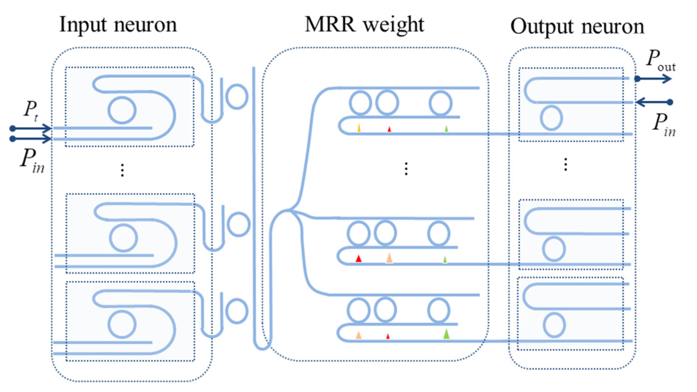
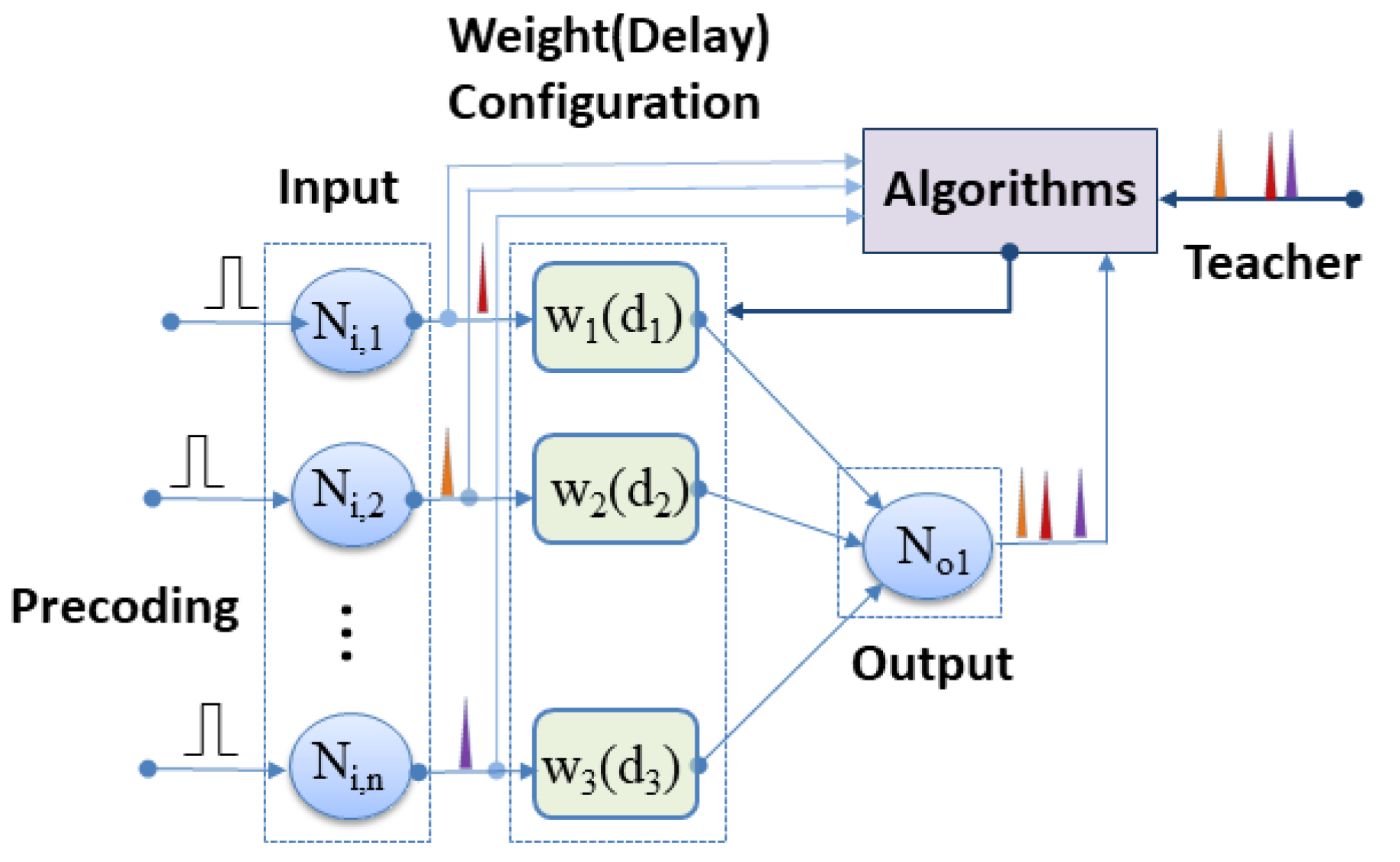
2. System-Level Computational Model

The proposed all-MRR-based photonic SNN architecture consists of the MRR-based neurons and synapses. A schematic structure of an all-coupling SNN is presented in Figure 1. The input data are firstly pre-coded into different spiking times at different wavelengths and sent to the input MRR neurons, the outputs of which are then multiplexed via a bus waveguide, and then split into several parts according to the number of input and output neurons. The central part is the MRR weight unit, through which the coupling strength of all pre-post neuron pairs could be adjusted, and results will be obtained from the spikes generated by the output neurons. In the following, we will, respectively, discuss the mechanisms of MRR based neurons, weight elements and STDP function.

2.1. MRR-Based Photonic Neuron

Photonic neurons based on MRR are actually passive devices and require external continuous wave injection acts as pump light for the generation of spiking dynamics, such as self-pulsations [51,52]. Due to the nonlinear effects of silicon materials, such as two-photon absorption (TPA), free carrier absorption (FCA) effect, free carrier dispersion (FCD) effect, Kerr effect, and thermo-optic effect, self-pulsations occur as the change of resonance frequency of the MRR and the light intensity, as was illustrated in detail in Refs. [47,48,49,50]. We proposed a novel structure of photonic spiking neurons based on add-drop MRR, as shown in Figure 2a. The normalized dimensionless nonlinear rate Equations can be derived as [49,50,51,53]:
d a d t = P i n + P t + δ a j n k e r r _ N | a | 2 a + j ( n + σ F C D n 0.8 ) a ( 1 + γ F C A n ) a α T P A | a | 2 a ( 1 / ( 1 + | a | 2 / W s a t ) ) a
d n d t = n τ f c + | a | 4
b o u t = P i n Γ c a
The time t is normalized via Γ 0 = ω 0 / ( 2 Q L ) , where Q L is the loaded quality factor of the system. For critical coupling, there is 1 / ( Q L ) = 1 / ( Q E ) + 1 / ( Q 0 ) , where Q E ( Q 0 ) is external (inner) quality factor. Here, a is the normalized complex light amplitude in the MRR. P i n is the injection power and P t denotes the perturbation. Note, that in the add-drop configuration, P i n and P t are sent into different ports of MRR, compared with the all-pass configuration utilized in [47,54]. δ = λ i λ 0 is the difference between the input light wavelength and the resonant wavelength. n k e r r _ N is the Kerr coefficient of silicon and Graphene [54]. σ F C D is related to the FCD effect, γ F C A and α T P A is, respectively, the FCA absorption coefficient and TPA coefficient. W s a t is the total energy stored in the cavity at the onset of saturable absorption [55,56]. τ f c is the normalized carrier lifetime, and n is the normalized carrier density. b o u t is the output complex light amplitude, and Γ c = ω 0 / Q e describes the coupling coefficient. The thermo-optic effect is assumed to be constant for fast (GHz) signals due to the large time constant. The detailed parameters used are given in Table 1.
The self-pulsation dynamic is demonstrated in Figure 2b,c for different injection strengths. Action potentials are generated in a certain frequency band, indicating class 2 neural excitability. When working below the self-pulsation threshold and injected via an optical perturbation pulse, the MRR neuron generates a positive spike, as shown in Figure 3. Note, in Figure 3a1,b1, two adjacent input pulses lead to only one spike, which is a result of a relatively larger rising edge duration of the spike due to relatively weak stimulation, not in a concept of “integration”. Those two input pulses can, respectively, trigger a spike, as shown in Figure 3a2,b2. Figure 3a3,b3 shows multiple spike generation with wider rectangular pulse injection, indicating pulse energy encoding. The MRR-based neuron model is considered to be “resonate and fire” neuron, which has not a clear threshold of firing and shows damped subthreshold oscillations [57].
In addition, the input frequency may also have impacts on the spiking dynamics of the proposed neuron. We vary the frequency offset δ to observe the output signal and find that within about −300 pm to 300 pm, a clear pulse could be generated. However, the output amplitude decays as |δ| increases, as shown in Figure 4a. Figure 4b gives the threshold property of the proposed add-drop MRR neuron. For the input power from 0 to 0.03, the slope of the output power is higher, which indicates the quasi-threshold property that is called after FitzHugh [58]. For integrating and firing neurons there is a specific threshold of spiking, that is, when the perturbation pulse is above the threshold, the neuron fires a spike or otherwise remains quiescent. However, the MRR neuron generates a spike as soon as the perturbation occurs despite the input strength, as shown in Figure 3c1–c3. Compared with the VCSEL-SA based optical neuron, the MRR based neuron lacks integration, a well-defined threshold and spike latency. However, these are important mechanisms related to learning in optical temporal-encoded SNN in our previous works [12]. With integration, the neuron first accumulates input energy, and there will be a latency between the input and the output that can be obviously adjusted via the input strength. This is especially important in temporal encoding neural networks because in such a network the spike timing conveys information. Moreover, a clear threshold means we have a one-or-none spike transmitted in the neural network. Since the MRR neuron lacks a clear threshold, a proper value could be set as “threshold.” However, it might bring more ambiguity to the network.

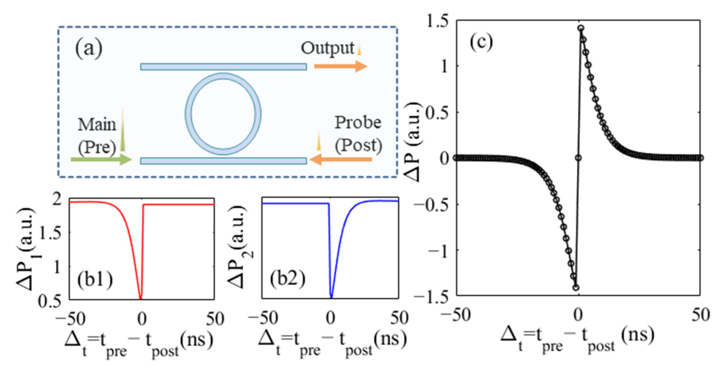
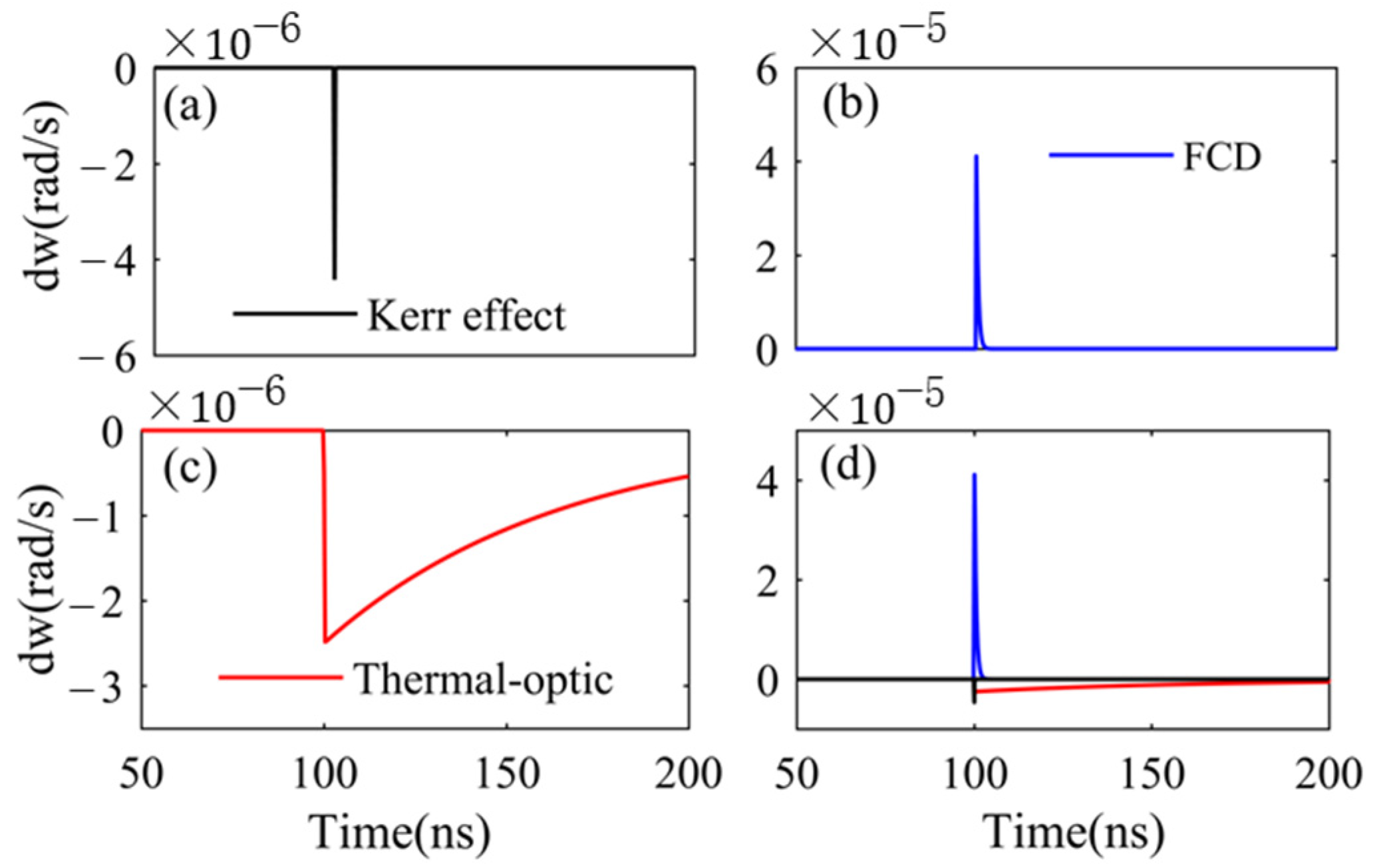
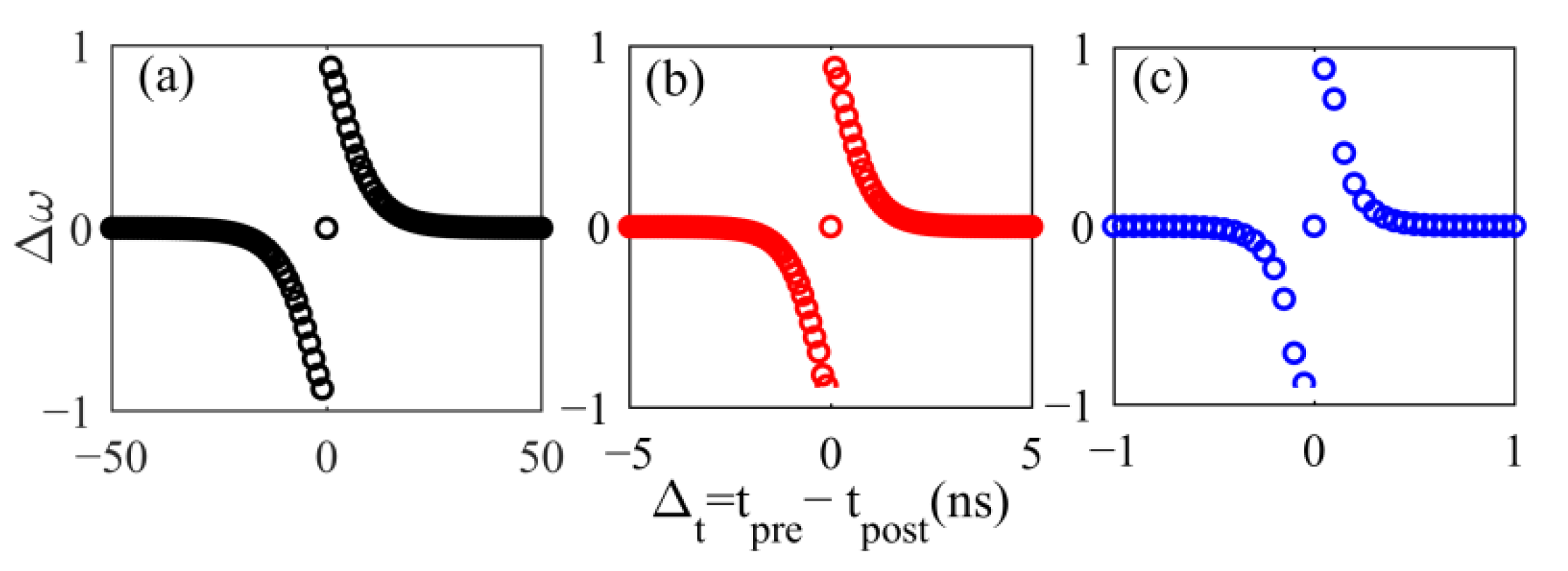
2.2. MRR-Based Optical Synaptic Plasticity

STDP is a Hebbian synaptic learning rule demonstrated in various neural circuits. The dependence of synaptic modification on the spiking time between pre- and postsynaptic spikes is considered to have profound functional implications [22]. On the basis of the intra-cavity nonlinear effect, a MRR-based STDP scheme has already been reported [34]. Here, we introduce an optical STDP scheme based on MRRs as shown in Figure 5a. The derived rate Equations are as follows [47,48,59]:
d A ± d t = [ j ( ω r + δ ω n l ω ± ) γ l o s s 2 ] A ± + κ ± S ±
d Δ T d t = Δ T τ t h + Γ t h P a b s ρ S i c p , S i V t h  
d N d t = N τ f c + Γ F C A β S i c 2 2 h ¯ ω V F C A 2 n g 2 ( | A + | 4 + 4 | A + | 2 | A | 2 + | A | 4 )  
where A ± denotes the complex amplitude of the forward and backward propagation mode. ω ± = 2 π c / λ ± is the frequency of input light in the waveguide, δ ω n l = ω r ( Δ n i , K e r r + Δ n i , F C D + Δ n i , t h ) / n S i is the resonant wavelength detuning caused by the Kerr effect, FCD and thermo-optic effect. γ l o s s is the total loss in the cavity, including coupling loss, radiation loss and absorption loss. κ ± represents the coupling coefficient, and S ± stands for the input light amplitude. Δ T is the temperature difference with the surroundings and denotes the free carrier density. P a b s describes the total absorption, including linear surface absorption, TPA and FCA. β S i is the constant governing TPA. h ¯ = h / ( 2 π ) is the reduced Planck constant. Detailed parameters are given in Table 2.
The concept of optical two-neuron synaptic systems is similar: a spike with relatively higher energy is used to generate a nonlinear effect that decays over time while monitoring the output of a lower energy spike that is fed into the system at varying times. Here, as an example, we firstly set the pre-synaptic spike as the main signal, denoted as Pre, and the post-synaptic spike as a weak probe signal, denoted by Post. The power of the Post and Pre could be set as, for example, P p r e = 20   m W ,   P p o s t = 2   m W (the power ratio is 10:1), by which the STDP-like function could be successfully produced. If the Post arrives before the Pre, it will not be affected via the nonlinear effects caused by the Pre and the output power will remain constant. However, if the Post arrives after the Pre, the strong power of the latter will cause a significant increase in the population of free carriers due to TPA, which will further lead to FCD and causes a blue shift in the resonant wavelength. The Kerr effect, as well as the thermo-optic effect caused by absorptions, will lead to a redshift in the resonant wavelength. The transmission of the weak Post spike will be affected by these nonlinear effects, and gradually returns over time, as shown in Figure 5b1. For a more detailed description, the frequency detuning caused via the Kerr effect, FCD and thermo-optic effect are, respectively, presented in Figure 6a–c and shown together in Figure 6d for an intuitive observation of the nonlinear effect strength. It can be seen that FCD is the dominant effect in the MRR. Then if we utilize Post as the main signal and Pre as the probe in another identical MRR, a symmetric transmission is acquired, as shown in Figure 5b2. Combining the transmission of both MRRs and subtracting their response, namely Δ P = Δ P 1 Δ P 2 , the STDP transfer function will be obtained as in Figure 5c.
The STDP window is governed by the relaxation time of free-carrier τ f c as can be seen in Figure 7, where Δ ω represents the normalized transmission. The required STDP window is mainly dependent on the FCD effect since it is dominant. Hence, we neglect the thermo-optic effect, because it has a relatively low but long-last impact on the inner state of MRR due to the large time constant (as can be seen in Figure 6d), which will lead to non-zero values outside the effective STDP window.

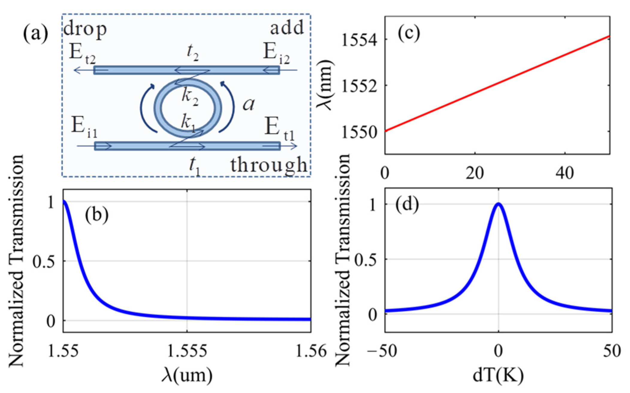
2.3. MRR Based Weight Configuration
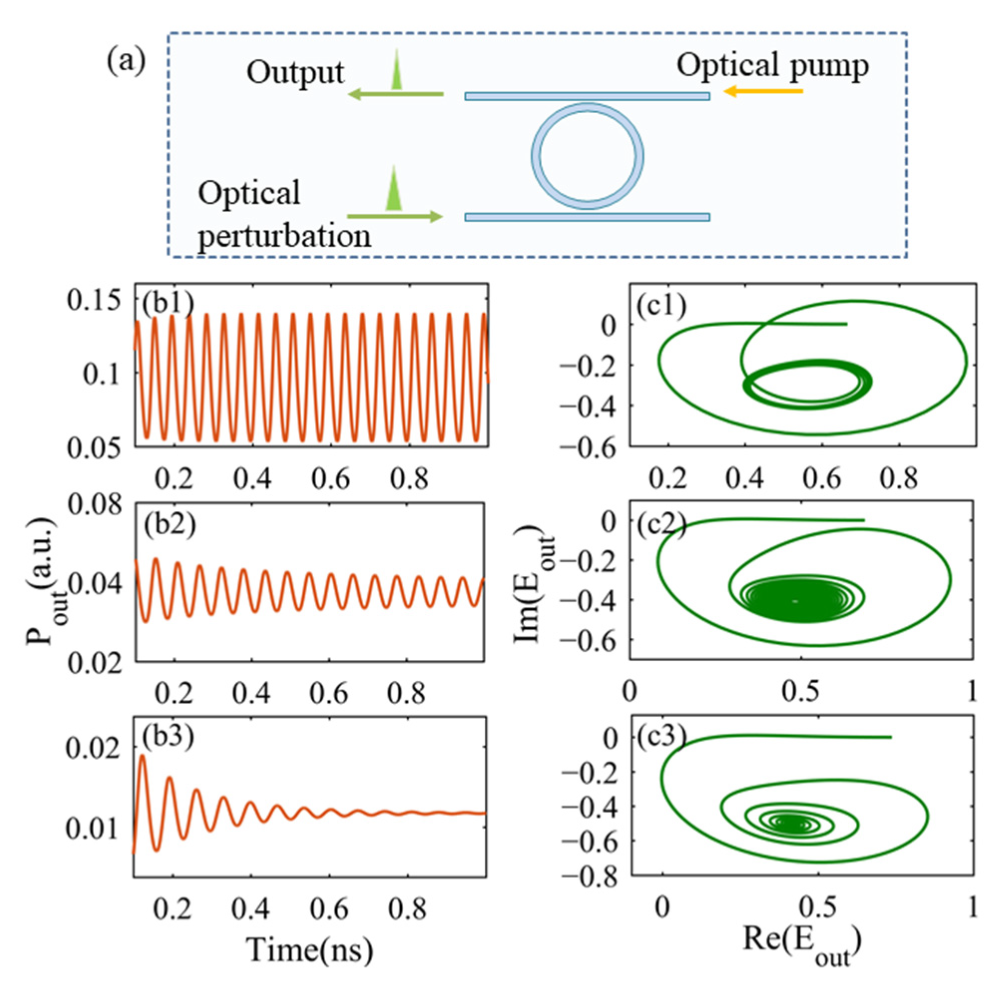
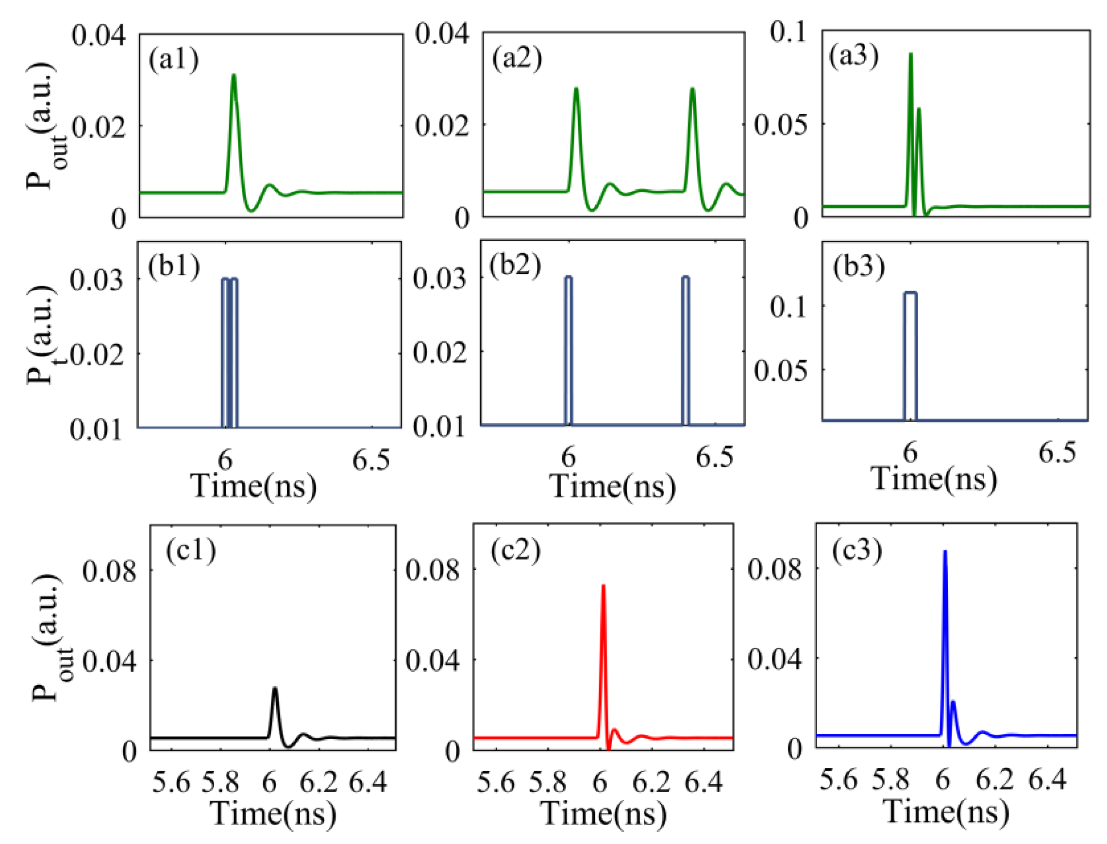
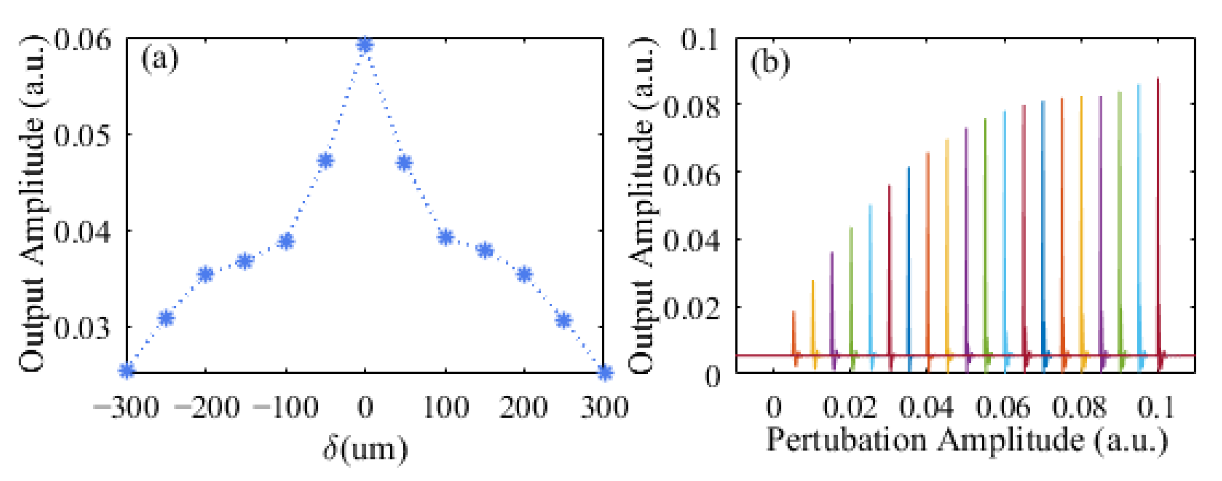
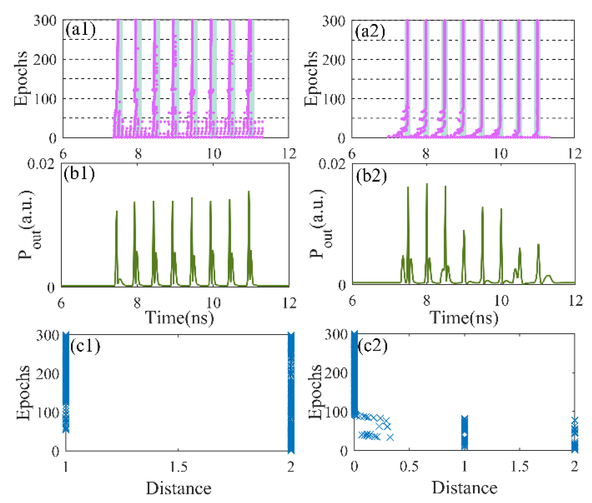
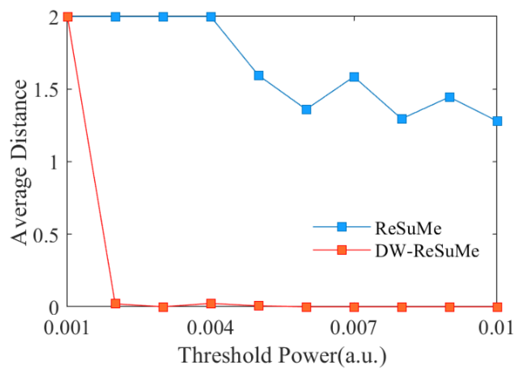
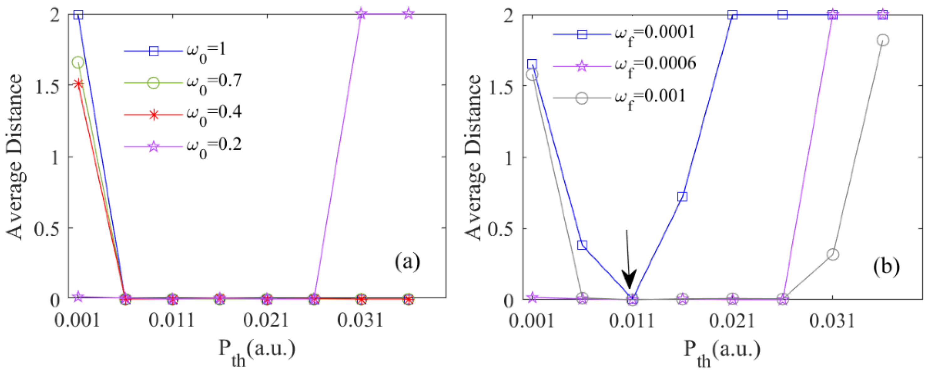
Thermal tuning is an effective way for resonant wavelength tuning of MRR due to the large thermo-optic coefficient. Consider an add-drop MRR configuration as shown in Figure 8a and according to coupled-mode theory, the transmission of the drop port can be derived as:
T d = | E t 2 2 | | E i 1 2 | = a 2 k 1 2 k 2 2 1 + a 4 t 1 2 t 2 2 2 a 2 t 1 t 2 cos ( 2 θ )
where θ = 1 / 2 β L = 2 π 2 R n e f f / λ is the phase change during half cycle propagation, and n e f f is the efficient refractive index. For simplicity, we only consider the effect on the silicon waveguide core. The effective index variation Δ n e f f is approximately a linear function of temperature change: Δ n e f f = Δ T d n / d T , where d n / d T is the thermo-optic coefficient and is about 1.86 × 10 4   K 1 at 1550 nm [36,40]. The wavelength shift is estimated to Δ λ = λ ( Δ T d n / d T ) / n g , and n g is the group refractive index.
The weight is modified according to the transmission of the drop port, which is a function of input light wavelength, as shown in Figure 8b. The resonant wavelength as a function of temperature shift is presented in Figure 8c. Via thermo-optic tuning, the transmission of the drop port can be adjusted within the range of [0,1], indicating weight configuration, as illustrated in Figure 8d. For applications, thermo-optic phase shifters could be typically implemented using metallic heaters (on-ring) [35] or doped-silicon resistive heaters (in ring) [37], which might acquire a suite of external measurement equipment dedicated for each MRR. In-resonator photoconductive heaters for both detection and control could alleviate the need for dedicated PDs [38,39]. In practice, the relationship between the desired weight and the applied voltage or current is usually previously measured for a direct configuration. Feedback control is usually adopted for stabilization and to obtain higher precision [43].
Moreover, it should be particularly pointed out that, the output waveform of an ultrashort optical pulse transmitted through MRR would be distorted because the transmission differs in wavelength (see Figure 8b). The frequency band of the input signal should be as narrow as possible compared to the falling edge of the transmission spectrum. This brings a tradeoff between the WDM channels and crosstalk, and a tradeoff between the speed (equivalently the spike width) and the weight precision. In addition, it still requires modification algorithms to compensate for weight accuracy. Here, for simplicity, we apply the weight configuration via a linear map of the normalized transmission.

3. Results

In this section, we use the Remote Supervised Method (ReSuMe) to implement a spike sequence learning task in the proposed SNN, which combines the MRR-based STDP with a 1 ns window. The weight is modified according to [12,15]:
Δ d i = ( D i d D i o ) ; D i d = t d t i , D i o = t o t i
d i ( x + 1 ) = d i ( x ) + η d Δ d i
The proposed learning architecture is presented in Figure 9. The input layer consists of 200 pre-synaptic MRR neurons, each connected to the single output neuron with a synapse. Temporal encoding is adopted, and the input signals are pre-encoded into rectangular pulses with a time interval of 0.02 ns, linearly increasing from 5.31 ns to 9.29 ns. The initial time delay is set to 2 ns for each synapse.
The results are given in Figure 10. It seems that the output spikes are near to the desired ones from the training process in Figure 10a1 and the final output in Figure 10b1. To quantitively describe the difference, we calculate the “distance” between the actual and desired spike sequences as in Ref. [15], and present the result in Figure 10c1. The distance is defined as:
Distance = 2 | n o n d + 1 | n o = n d , | t o t d | r + n o = n d | t o t d | < r ( | ( t o t d ) | / n o r )
The actual output could never reach the desired one because the weight does not contribute to the spiking time of the MRR-based neuron, as illustrated in Figure 3c1–c3. It seems that such neuron does not fit for temporal encoding in a SNN, but it could be useful for rate coding that encodes input energy into multiple spikes as demonstrated in Figure 3a3,b3, which deserves further investigation in future works. However, we address this issue via introducing delay learning in the traditional weight-based ReSuMe algorithm, which was described in our previous work [15]. The updating of synaptic delay is according to:
Δ d i = ( D i d D i o ) ; D i d = t d t i , D i o = t o t i
d i ( x + 1 ) = d i ( x ) + η d Δ d i
The results are presented in Figure 10a2–c2. We can see that combined with delayed learning; the actual output is exactly at the desired time. The learning process converges quickly and is quite stable. It should be noted that via MRR weight configuration, the coupling strength could not be increased, thereby, the weight of a synapse is confined within the range of [0,1]. Additionally, note that in our network, the presynaptic neurons are pre-coded into only one spike; however, the postsynaptic neuron may generate multiple spikes within the STDP window, thus, the weight modification would be affected by different pairs of pre-post spike pairs during the training process. We choose linear integration to perform the weight computing, that is, to sum up the modification of each spike pair [60]. In particular, the STDP curve used here is highly symmetric. However, in biological experiments, the LTP and LTD functions are usually asymmetric due to the complex mechanisms of biological neurons and synapses [61]. The optical implementation of asymmetric STDP and its influence on OSNN will deserve further exploration.
For further comparison, we calculate the average distance from epoch101 to epoch300 of the two algorithms with varying threshold power. The result is shown in Figure 11. We can see that with traditional ReSuMe, the distance is higher than 1 for all threshold powers, indicating the learning process could never converge. However, when combined with delay learning, the average distance can converge to 0 for a wide range of thresholds. The result suggests that with delay learning, the spike sequence learning could be successfully achieved via an MRR-based learning structure.
The initial weight and threshold power also have impacts on the performance. As the weight can be adjusted within 0–1, we select different initial weights ( ω 0 = 1 ,   0.7 ,   0.4 ,   0.2 ) for a brief comparison. A relatively small learning rate usually contribute to better performance in the delay combined algorithm [15], so we choose ω f = 0.0006 . The average distance is calculated as a function of threshold power in Figure 12a. We can see that with a relatively larger initial weight, the average distance is close to 0 for a relatively higher threshold power. As the initial weight ω 0 decreases, the training process gradually becomes convergent for a low threshold power ( P t h = 0.001 ). However, a low ω 0 also makes it fail to converge with higher threshold power ( P t h = 0.031 ,   0.036 ). In Figure 12b, we also compare the performance of different learning rates. The result indicates that the learning process is highly modified by the learning rate ω f , and a proper ω f is required for better performance. Note, that a relatively higher ω f can also lead to faster convergence. At the point marked in Figure 12b, for all the considered ω f , the average distance approaches 0. The related convergent epoch, defined here as the first training epoch that corresponds to a distance less than 0.1 is, respectively, 116, 64 and 62 for ω f = 0.0001 ,   0.0006 ,   and   0.001 .

4. Conclusions

In summary, we proposed an all-MRR-based photonic SNN architecture. On account of the nonlinear effects in silicon, the neuron-like dynamics, photonic STDP, as well as weighting, could be realized based on the MRRs. Furthermore, with a supervised learning algorithm, we also achieved the spike sequence learning in the proposed architecture.
The MRR based architecture provides potential approaches to the realization and application of large-scale neural networks because it is not only CMOS-compatible but has internal WDM properties and small footprints.
Note, in addition to the hardware devices, the algorithm also plays important role in a SNN, which combines together the spiking properties of neurons, the encoding schemes and the specific problems to be solved. For the moment, hardware implementations are more suitable for online inference rather than online learning. The weight calculation and updating during training largely rely on electronic control. A generalized and robust algorithm might be able to compensate for some of the limitations and shortcomings of photonic hardware and promote the development and applications of photonic SNN.

Author Contributions

Conceptualization, S.X. and Y.H. (Yanan Han); methodology, Y.H. (Yanan Han) and Y.Z.; investigation and data curation, Y.H. (Yanan Han); writing—original draft preparation, Y.H. (Yanan Han); writing—review and editing, S.X.; visualization, S.G. and Y.Z.; supervision, A.W. and Y.H (Yue Hao).; funding acquisition, S.X. All authors have read and agreed to the published version of the manuscript.

Funding

This work is supported by the National Key Research and Development Program of China (2021YFB2801900, 2021YFB2801901,2021YFB2801902, 2021YFB2801903, 2021YFB2801904), the National Outstanding Youth Science Fund Project of National Natural Science Foundation of China (62022062), the National Natural Science Foundation of China (61974177, 61674119), and the Fundamental Research Funds for the Central Universities (JB210114).

Institutional Review Board Statement

Not applicable.

Informed Consent Statement

Not applicable.

Data Availability Statement

The data presented in this study are available on request from the corresponding author.

Conflicts of Interest

The authors declare no conflict of interest.

References

  1. Furber, S.B.; Galluppi, F.; Temple, S.; Plana, L.A. The SpiNNaker project. Proc. IEEE 2014, 102, 652–665. [Google Scholar] [CrossRef]
  2. Akopyan, F.; Sawada, J.; Cassidy, A.; Alvarez-Icaza, R.; Arthur, J.; Merolla, P.; Imam, N.; Nakamura, Y.; Datta, P.; Nam, G.; et al. TrueNorth: Design and tool flow of a 65 mW 1 million neuron programmable neurosynaptic chip. IEEE Trans. Comput.-Aided Des. Integr. Circuits Syst. 2015, 34, 1537–1557. [Google Scholar] [CrossRef]
  3. Jouppi, N.P.; Young, C.; Patil, N.; Patterson, D.; Agrawal, G.; Bajwa, R.; Bates, S.; Bhatia, S.; Boden, N.; Borchers, A.; et al. In-datacenter performance analysis of a tensor processing unit. In Proceedings of the 44th Annual International Symposium on Computer Architecture, Toronto, ON, Canada, 24–28 June 2017. [Google Scholar]
  4. Hurtado, A.; Schires, K.; Henning, I.D.; Adams, M.J. Investigation of vertical cavity surface emitting laser dynamics for neuromorphic photonic systems. Appl. Phys. Lett. 2012, 100, 103703. [Google Scholar] [CrossRef] [Green Version]
  5. Li, Q.; Wang, Z.; Le, Y.; Sun, C.; Song, X.; Wu, C. Optical implementation of neural learning algorithms based on cross-gain modulation in a semiconductor optical amplifier. Proc. SPIE 2016, 10019, 1–7. [Google Scholar]
  6. Xiang, S.Y.; Zhang, H.; Guo, X.X.; Li, J.F.; Wen, A.J.; Pan, W.; Hao, Y. Cascadable neuron-Like spiking dynamics in coupled VCSELs subject to orthogonally polarized optical pulse injection. IEEE J. Sel. Topics Quantum Electron. 2017, 23, 1700207. [Google Scholar] [CrossRef]
  7. Deng, T.; Robertson, J.; Hurtado, A. Controlled propagation of spiking dynamics in vertical-cavity surface-emitting lasers: Towards neuromorphic photonic networks. IEEE J. Sel. Top. Quantum Electron. 2017, 23, 1800408. [Google Scholar] [CrossRef] [Green Version]
  8. Chen, Z.G.; Carlos, R.; Pernice, W.H.P.; Wright, C.D.; Bhaskara, H. On-chip photonic synapse. Sci. Adv. 2017, 3, e1700160. [Google Scholar] [CrossRef] [PubMed] [Green Version]
  9. Ríos, C.; Youngblood, N.; Cheng, Z.G.; Gallo, M.L.; Pernice, W.H.P.; Wright, C.D.; Sebastian, A.; Bhaskaran, H. In-memory computing on a photonic platform. Sci. Adv. 2019, 5, eaau5759. [Google Scholar] [CrossRef] [PubMed] [Green Version]
  10. Chakraborty, I.; Saha, G.; Roy, K. Photonic in-memory computing primitive for spiking neural networks using phase-change materials. Phys. Rev. Appl. 2019, 11, 014063. [Google Scholar] [CrossRef] [Green Version]
  11. Xiang, S.Y.; Zhang, Y.H.; Gong, J.K.; Guo, X.X.; Lin, L.; Hao, Y. STDP-based unsupervised spike pattern learning in a photonic spiking neural network with VCSELs and VCSOAs. IEEE J. Sel. Top. Quantum Electron. 2019, 25, 1700109. [Google Scholar] [CrossRef]
  12. Xiang, S.Y.; Ren, Z.X.; Song, Z.W.; Zhang, Y.H.; Guo, X.X.; Han, G.Q.; Hao, Y. Computing primitive of fully-VCSELs-based all-optical spiking neural network for supervised learning and pattern classification. IEEE Trans. Neural Netw. Learn. Syst. 2021, 32, 2494–2505. [Google Scholar] [CrossRef] [PubMed]
  13. Pammi, V.A.; Alfaro-Bittner, K.; Clerc, M.G.; Barbay, S. Photonic computing with single and coupled spiking micropillar lasers. IEEE J. Sel. Top. Quantum Electron. 2020, 26, 1500307. [Google Scholar] [CrossRef] [Green Version]
  14. Guo, X.H.; Xiang, J.L.; Zhang, Y.J.; Su, Y.K. Integrated neuromorphic photonics: Synapses, neurons, and neural networks. Adv. Photonics Res. 2021, 2, 2000212. [Google Scholar] [CrossRef]
  15. Han, Y.N.; Xiang, S.Y.; Ren, Z.X.; Fu, C.T.; Wen, A.J.; Hao, Y. Delay-weight plasticity-based supervised learning in optical spiking neural networks. Photonics Res. 2021, 9, B119–B127. [Google Scholar] [CrossRef]
  16. Shastri, B.J.; Tait, A.N.; de Lima, T.F.; Pernice, W.H.P.; Bhaskaran, H.; Wright, C.D.; Prucnal, P.R. Photonics for artificial intelligence and neuromorphic computing. Nat. Photonics 2021, 15, 102–114. [Google Scholar] [CrossRef]
  17. Li, Q.; Wang, Z.; Cui, C.; Li, R.Q.; Li, Y.; Liu, B.; Wu, C.Q. Simulating the spiking response of VCSEL-based optical spiking neuron. Opt. Commun. 2018, 407, 327–332. [Google Scholar] [CrossRef]
  18. Mesaritakis, C.; Kapsalis, A.; Bogris, A.; Syvridis, D. Artificial neuron based on integrated semiconductor quantum dot mode-locked lasers. Sci. Rep. 2016, 6, 39317. [Google Scholar] [CrossRef]
  19. Zhang, Y.H.; Xiang, S.Y.; Guo, X.X.; Wen, A.J.; Hao, Y. All-optical inhibitory dynamics in photonic neuron based on polarization mode competition in a VCSEL with an embedded saturable absorber. Opt. Lett. 2019, 44, 1548–1551. [Google Scholar] [CrossRef]
  20. Ren, Q.; Zhang, Y.; Wang, R.; Zhao, J. Optical spike-timing-dependent plasticity with weight-dependent learning window and reward modulation. Opt. Express 2015, 23, 25247–25258. [Google Scholar] [CrossRef]
  21. Xiang, S.Y.; Gong, J.K.; Zhang, Y.H.; Guo, X.X.; Wen, A.J.; Hao, Y. Numerical implementation of wavelength-dependent photonic spike timing dependent plasticity based on VCSOA. IEEE J. Quantum Electron. 2018, 54, 8100107. [Google Scholar] [CrossRef]
  22. Caporale, N.; Yang, D. Spike timing-dependent plasticity: A hebbian learning rule. Annu. Rev. Neurosci. 2008, 31, 25–46. [Google Scholar] [CrossRef] [PubMed] [Green Version]
  23. Bi, G.-Q.; Poo, M.-M. Synaptic modifications in cultured hippocampal neurons: Dependence on spike timing, synaptic strength, and postsynaptic cell type. J. Neurosci. 1998, 18, 10464–10472. [Google Scholar] [CrossRef] [PubMed]
  24. Ferré, P.; Mamalet, F.; Thorpe, S.J. Unsupervised feature learning with winner-takes-all based STDP. Front. Comput. Neurosci. 2018, 12, 00024. [Google Scholar] [CrossRef] [PubMed] [Green Version]
  25. Kheradpisheh, S.R.; Ganjtabesh, M.; Thorpe, S.J.; Masquelier, T. STDP-based spiking deep convolutional neural networks for object recognition. Neural Netw. 2018, 99, 56–67. [Google Scholar] [CrossRef] [Green Version]
  26. Taherkhani, A.; Belatreche, A.; Li, Y.; Maguire, L.P. A supervised learning algorithm for learning precise timing of multiple spikes in multilayer spiking neural networks. IEEE Trans. Neural Netw. Learn. Syst. 2018, 29, 5394–5407. [Google Scholar] [CrossRef] [Green Version]
  27. Brehm, M. Silicon Photonics IV—Innovative Frontiers; Lockwood, D.J., Pavesi, L., Eds.; Springer: Berlin/Heidelberg, Germany, 2021; pp. 1–103. [Google Scholar]
  28. Carrillo, S.G.-C.; Lugnan, A.; Gemo, E.; Bienstman, P.; Pernice, W.H.P.; Bhaskaran, H.; Wright, C.D. System-level simulation for integrated phase-change photonics. J. Light. Technol. 2021, 39, 6392–6402. [Google Scholar] [CrossRef]
  29. Zhang, W.F.; Yao, J.P. A fully reconfigurable waveguide Bragg grating for programmable photonic signal processing. Nat. Commun. 2018, 9, 1396. [Google Scholar] [CrossRef]
  30. Zhang, H.; Gu, M.; Jiang, X.D.; Thompson, J.; Cai, H.; Paesani, S.; Santagati, R.; Laing, A.; Zhang, Y.; Yung, M.H.; et al. An optical neural chip for implementing complex-valued neural network. Nat. Commun. 2021, 12, 457. [Google Scholar] [CrossRef]
  31. Xu, X.Y.; Tan, M.X.; Corcoran, B.; Wu, J.Y.; Boes, A.; Nguyen, T.G.; Chu, S.T.; Little, B.E.; Hicks, D.G.; Morandotti, R.; et al. 11 TOPS photonic convolutional accelerator for optical neural networks. Nature 2021, 589, 44–51. [Google Scholar] [CrossRef]
  32. Feldmann, J.; Youngblood, N.; Karpov, M.; Gehring, H.; Li, X.; Stappers, M.; Gallo, M.L.; Fu, X.; Lukashchuk, A.; Raja, A.S. Parallel convolutional processing using an integrated photonic tensor core. Nature 2021, 589, 52–58. [Google Scholar] [CrossRef]
  33. Feldmann, J.; Youngblood, N.; Wright, C.D.; Bhaskaran, H.; Pernice, W.H. All-optical spiking neurosynaptic networks with self-learning capabilities. Nature 2019, 569, 208–214. [Google Scholar] [CrossRef] [Green Version]
  34. Mesaritakis, C.; Skontranis, M.; Sarantoglou, G.; Bogris, A. Micro-ring-resonator based passive photonic spike-time-dependent-plasticity scheme for unsupervised learning in optical neural networks. In Proceedings of the 2020 Optical Fiber Communications Conference and Exhibition (OFC), San Diego, CA, USA, 8–12 March 2020. [Google Scholar]
  35. Grillanda, S.; Carminati, M.; Morichetti, F.; Ciccarella, P.; Annoni, A.; Ferrari, G.; Strain, M.; Sorel, M.; Sampietro, M.; Melloni, A. Non-invasive monitoring and control in silicon photonics using CMOS integrated electronics. Optica 2014, 1, 129–136. [Google Scholar] [CrossRef] [Green Version]
  36. Zhang, Y.; Li, Y.; Feng, S.Q.; Poon, A.W. Towards adaptively tuned silicon microring resonators for optical networks-on-chip applications. IEEE J. Sel. Top. Quantum Electron. 2014, 20, 136–149. [Google Scholar] [CrossRef]
  37. Li, Y.; Poon, A.W. Active resonance wavelength stabilization for silicon microring resonators with an in-resonator defect-state-absorption-based photodetector. Opt. Express 2015, 23, 360–372. [Google Scholar] [CrossRef] [PubMed]
  38. Poulton, C.V.; Dong, P.; Chen, Y.K. Photo resistive micro ring heater with resonance control loop. In Proceedings of the CLEO: Science and Innovations, San Jose, CA, USA, 10–15 May 2015; Optical Society of America: Holmdel, NJ, USA, 2015; p. SM2I.3. [Google Scholar]
  39. Hasitha, J.; Kyle, M.; Guillén-Torres, M.A.; Michael, C.; Ricky, H.; Jaeger, N.A.F.; Chrostowski, L.; Shekhar, S. Wavelength tuning and stabilization of microring-based filters using silicon in-resonator photoconductive heaters. Opt. Express 2015, 23, 25084–25097. [Google Scholar]
  40. Pintus, P.; Hofbauer, M.; Manganelli, C.L.; Fournier, M.; Gundavarapu, S.; Lemonnier, O.; Gambini, F.; Adelmini, L.; Meinhart, C.; Kopp, C.; et al. PWM-driven thermally tunable silicon microring resonators: Design, fabrication, and characterization. Laser Photonics Rev. 2019, 13, 1800275. [Google Scholar] [CrossRef]
  41. Bangari, V.; Marquez, B.A.; Miller, H.; Tait, A.N.; Nahmias, M.A.; De Lima, T.F.; Peng, H.-T.; Prucnal, P.R.; Shastri, B.J. Digital electronics and analog photonics for convolutional neural networks (DEAP-CNNs). IEEE J. Sel. Top. Quantum Electron. 2019, 26, 1–13. [Google Scholar] [CrossRef] [Green Version]
  42. Sunny, F.; Mirza, A.; Nikdast, M.; Pasricha, S. CrossLight: A cross-layer optimized silicon photonic neural network accelerator. arXiv 2021, arXiv:2102.06960. [Google Scholar]
  43. Tait, A.N.; de Lima, T.F.; Nahmias, M.A.; Shastri, B.J.; Prucnal, P.R. Multi-channel control for microring weight banks. Opt. Express 2016, 24, 008895. [Google Scholar] [CrossRef]
  44. Zhang, W.P.; Huang, C.R.; Bilodeau, S.; Jha, A.; Blow, E.; De Lima, T.F.; Shastri, B.J.; Prucnal, P. Microring weight banks control beyond 8.5-bits accuracy. arXiv 2021, arXiv:2104.01164. [Google Scholar]
  45. Jiang, Y.; Zhang, W.J.; Yang, F.; He, Z.Y. Photonic convolution neural network based on interleaved time-wavelength modulation. J. Light. Technol. 2021, 39, 4592–4600. [Google Scholar] [CrossRef]
  46. Chakraborty, I.; Saha, G.; Sengupta, A.; Roy, K. Toward fast neural computing using all-photonic phase change spiking neurons. Sci. Rep. 2018, 8, 12980. [Google Scholar] [CrossRef] [PubMed]
  47. Vaerenbergh, T.V.; Fiers, M.; Mechet, P.; Spuesens, T.; Kumar, R.; Morthier, G.; Schrauwen, B.; Dambre, J.; Bienstman, P. Cascadable excitability in microrings. Opt. Express 2012, 20, 20292–20308. [Google Scholar] [CrossRef] [Green Version]
  48. Xiang, J.L.; Torchy, A.; Guo, X.H.; Su, Y.K. All-optical spiking neuron based on passive microresonator. J. Light. Technol. 2020, 38, 4019–4029. [Google Scholar] [CrossRef]
  49. Jha, A.; Huang, C.R.; Peng, H.-T.; Shastri, B.; Prucnal, P.R. Photonic spiking neural networks and CMOS-compatible graphene-on-silicon spiking neurons. arXiv 2021, arXiv:2109.13797v1. [Google Scholar]
  50. Chen, S.W.; Zhang, L.B.; Fei, Y.H.; Cao, T.T. Bistability and self-pulsation phenomena in silicon microring resonators based on nonlinear optical effects. Opt. Express 2012, 20, 7454–7468. [Google Scholar] [CrossRef]
  51. Malaguti, S.; Bellanca, G.; de Rossi, A.; Combrié, S.; Trillo, S. Self-pulsing driven by two-photon absorption in semiconductor nanocavities. Phys. Rev. A 2011, 83, 051802. [Google Scholar] [CrossRef]
  52. Priem, G.; Dumon, P.; Bogaerts, W.; Thourhout, D.V.; Morthier, G.; Baets, R. Optical bistability and pulsating behaviour in Silicon-On-Insulator ring resonator structures. Opt. Express 2005, 13, 9623. [Google Scholar] [CrossRef] [Green Version]
  53. Haus, H.A.; Popović, M.A.; Watts, R.M.; Manolatou, C.; Little, E.B.; Chu, T.S. Optical resonators and filters. In Optical Microcavities; Advanced Series in Applied Physics; California Institute of Technology: California, CA, USA, 2004; pp. 1–37. [Google Scholar]
  54. Vermeulen, N.; David, C.L.; Cheng, J.L.; Pasternak, I.; Krajewska, A.; Ciuk, T.; Strupinski, W.; Thienpont, H.; Erps, J.V. Negative Kerr nonlinearity of graphene as seen via chirped-pulse-pumped self-phase modulation. Phys. Rev. Appl. 2016, 6, 044006. [Google Scholar] [CrossRef]
  55. Ataloglou, V.G.; Christopoulos, T.; Kriezis, E.E. Nonlinear coupled-mode theory framework for graphene-induced saturable absorption in nanophotonic resonant structures. Phys. Rev. A 2018, 97, 063836. [Google Scholar] [CrossRef]
  56. Chatzidimitriou, D.; Pitilakisa, A.; Kriezis, E.E. Rigorous calculation of nonlinear parameters in graphene-comprising waveguides. J. Appl. Phys. 2015, 118, 023105. [Google Scholar] [CrossRef] [Green Version]
  57. Izhikevich, E.M. Dynamical Systems in Neuroscience: The Geometry of Excitability and Bursting; The MIT Press: Cambridge, MA, USA; London, UK, 2007. [Google Scholar]
  58. FitzHugh, R. Mathematical models of threshold phenomena in the nerve membrane. Bull. Math. Biol. 1955, 17, 257–278. [Google Scholar] [CrossRef]
  59. Lin, Q.; Johnson, T.J.; Michael, C.P.; Painter, O. Adiabatic self-tuning in a silicon microdisk optical resonator. Opt. Express 2008, 16, 14801. [Google Scholar] [CrossRef] [PubMed] [Green Version]
  60. Froemke, R.; Dan, Y. Spike-timing dependent plasticity induced by natural spike trains. Nature 2002, 416, 433–438. [Google Scholar] [CrossRef] [PubMed]
  61. Pfister, J.P.; Gerstner, W. Triplets of Spikes in a Model of Spike Timing-Dependent Plasticity. J. Neurosci. 2006, 26, 9673–9682. [Google Scholar] [CrossRef] [Green Version]
Figure 1. The architecture of all-MRR-based photonic SNN.
Photonics 09 00120 g001
Figure 2. The proposed photonic neuron structure based on MRR (a); the output of the MRR neuron with P i n = 0.1 , 0.05 , 0.01 . (b1c3); the corresponding phase portrait of the normalized light complex amplitude (c1c3).
Photonics 09 00120 g002
Figure 3. The response of MRR neuron (a1a3) under external optical perturbation with different interval and duration time (b1b3). (c1c3) the output of MRR with perturbation strength P t = 0.01 , 0.05 , 0.1 , respectively.
Photonics 09 00120 g003
Figure 4. The frequency region of spiking dynamics (a); The quasi-threshold behavior of the proposed MRR-based neuron (b). The output spike is presented in the order in which the perturbation power increases.
Photonics 09 00120 g004
Figure 5. (a) MRR-based STDP structure; (b1,b2) the output power change as a function of Δ t ; (c) the calculated STDP transfer function.
Photonics 09 00120 g005
Figure 6. (ad): The resonance frequency detuning caused by the Kerr effect, FCD and thermo-optic effect as a function of time.
Photonics 09 00120 g006
Figure 7. STDP curve at different time scales (a) τ f c = 6.5   n s ; (b) τ f c = 0.5   n s ; (c τ f c = 0.2   n s .
Photonics 09 00120 g007
Figure 8. A basic structure of the add-drop MRR (a). The transmission of drop port as a function of input light wavelength (b). The resonant wavelength as a function of temperature shift (c). The transmission of the drop port indicates weight configuration as a function of temperature shift (d).
Photonics 09 00120 g008
Figure 9. The SNN learning structure.
Photonics 09 00120 g009
Figure 10. The spike sequence learning with different learning algorithms. (a1c1): The training process, the output spikes after the 300th training epoch, the calculated distance after each training epoch with ReSuMe method. (a2c2): with delay combined ReSuMe method. P_t = 0.032, ω_0 = 0.6, P_th = 0.006, w_f = 0.001.
Photonics 09 00120 g010
Figure 11. The average distance from epoch101 to epoch300 as a function of threshold power with the two learning algorithms.
Photonics 09 00120 g011
Figure 12. The average distance from epoch201 to epoch300 as a function of threshold power for different cases of initial weight ω 0 (a). The other parameters are: ω f = 0.0006 ,   P t = 0.0032 ; The average distance as a function of P t with ω f = 0.0001 , 0.0006 ,   and   0.001 , respectively (b).
Photonics 09 00120 g012
Table 1. Basic Parameters Used in MRR neuron model.
ParameterValueUnitRefs
n S i = n g 3.476 [47,48]
Γ F C A 0.9996 [47]
V t h 3.81 μ m 3 [47]
n 2 I 4.5 × 10 18 m 2 / W [48,49,50]
n 2 I G 1 × 10 13 m 2 / W [49,54]
η 0 120 π Ω [55,56]
Q 0 60,000
Q e 30,000
I s a t 1 MW / cm 2 [49,55]
Table 2. Basic Parameters Used in MRR STDP.
ParameterValueUnitRefs
n S i = n g 3.476 [47,48]
β S i 0.75 × 10 11 m W 1 [50]
d n S i / d T 1.86 × 10 4 K 1 [47,48]
d n S i / d N 1.73 × 10 27 m 3 [47]
τ t h 65 ns [47,48,52]
Γ t h 0.934 [48]
Γ T P A 0.995 [48]
Γ F C A 0.998 [48]
V t h 3.81 μ m 3 [47]
V T P A 3.09 μ m 3 [48]
V F C A 2.82 μ m 3 [48]
c p , S i 0.7 J g 1 K 1 [47]
ρ S i 2.33 g cm 3 [47]
σ FCA 1.45 × 10 23 [50]
h 6.63 × 10 34 J s
Publisher’s Note: MDPI stays neutral with regard to jurisdictional claims in published maps and institutional affiliations.

