1. Introduction
Quantum cascade lasers (QCL) are nowadays considered the most versatile sources of coherent light. These devices can operate in an extremely large spectral range from the mid-infrared to THz. The couple InAs/AlSb is the most recent QCL material family compared to alloys grown on InP and GaAs substrates. The main advantage of the InAs/AlSb material system is the small effective electron mass in quantum wells, which favors a high intersubband gain [
1]. This benefit can be better exploited in long-wavelength QCLs where the lasing transition levels are close to the bottom of the conduction band and the effect of nonparabolicity is weak. InAs-based QCLs demonstrated room temperature (RT) continuous wave (cw) operation at wavelengths up to 17.7 µm with a pulsed threshold current density
Jth as low as 1.0 kA/cm
2 [
2]. Low values of
Jth were also achieved in InAs-based QCLs emitting in other spectral regions: 0.715 kA/cm
2 at 15 µm [
3], 0.99 kA/cm
2 at 11 µm [
4] and 0.75 kA/cm
2 at 7.7 µm [
5] (QCL grown on InAs). These performances are significantly better than those demonstrated in QCLs based on other materials. The longest wavelength of pulsed RT operation of InP-based QCLs is below 16 µm with
Jth of ~10 kA/cm
2 at 15.6 µm [
6] and 8.94 kA/cm
2 at 15.5 µm [
7]. Lower
Jth values were obtained in InP-based QCLs operating at shorter wavelengths: 3.5 kA/cm
2 at 15 µm [
8], 2.0 kA/cm
2 at 14 µm [
9], and 1.45 kA/cm
2 at 7.1 µm [
10]. An extremely low threshold current density of 0.47 kA/cm
2 has been reached in lasers with HR-coated back facets emitting at 4.6 µm (0.715 kA/cm
2 in uncoated devices), in the spectral range of the best performance of InP-based QCLs [
11].
The considerable improvement in
Jth of long-wavelength InAs-based QCLs compared to the previous generation [
12,
13] was achieved in a large part by decreasing the active region doping, resulting in a reduction in the resonant loss and free carrier absorption. Typically, two of ten InAs quantum wells in the middle of the active region were doped to just 2 × 10
16 cm
−3 in these lasers [
3]. However, low doping makes such devices very sensitive to non-intentional residual doping, which can vary from low 10
15 to 10
16 cm
−3 in InAs QWs depending on growth conditions and the overall state of the growth equipment. Another drawback of the approach used is the relatively small energy distance of about 50 meV between the upper transition level e3 and the next one e4 in active quantum wells. Undesired recombination of electrons thermally excited from e3 to e4 negatively affects QCL performance [
14]. In this work, we present one of the possible directions for the further development of long-wavelength InAs-based QCLs.
2. Methods and Materials
In the QCL active region a large part of electrons thermally activated from e3 to e4 come back to the upper lasing level whereas their direct recombination to lower states in the active region results in shortening of the lasing transition [
14]. In the presence of elastic scattering, such as interface scattering and alloy disordering, the undesired effect of this recombination path becomes stronger, further reducing the lasing efficiency [
14]. A larger e3–e4 distance is required to improve laser performance. The vertical design used, for example, in [
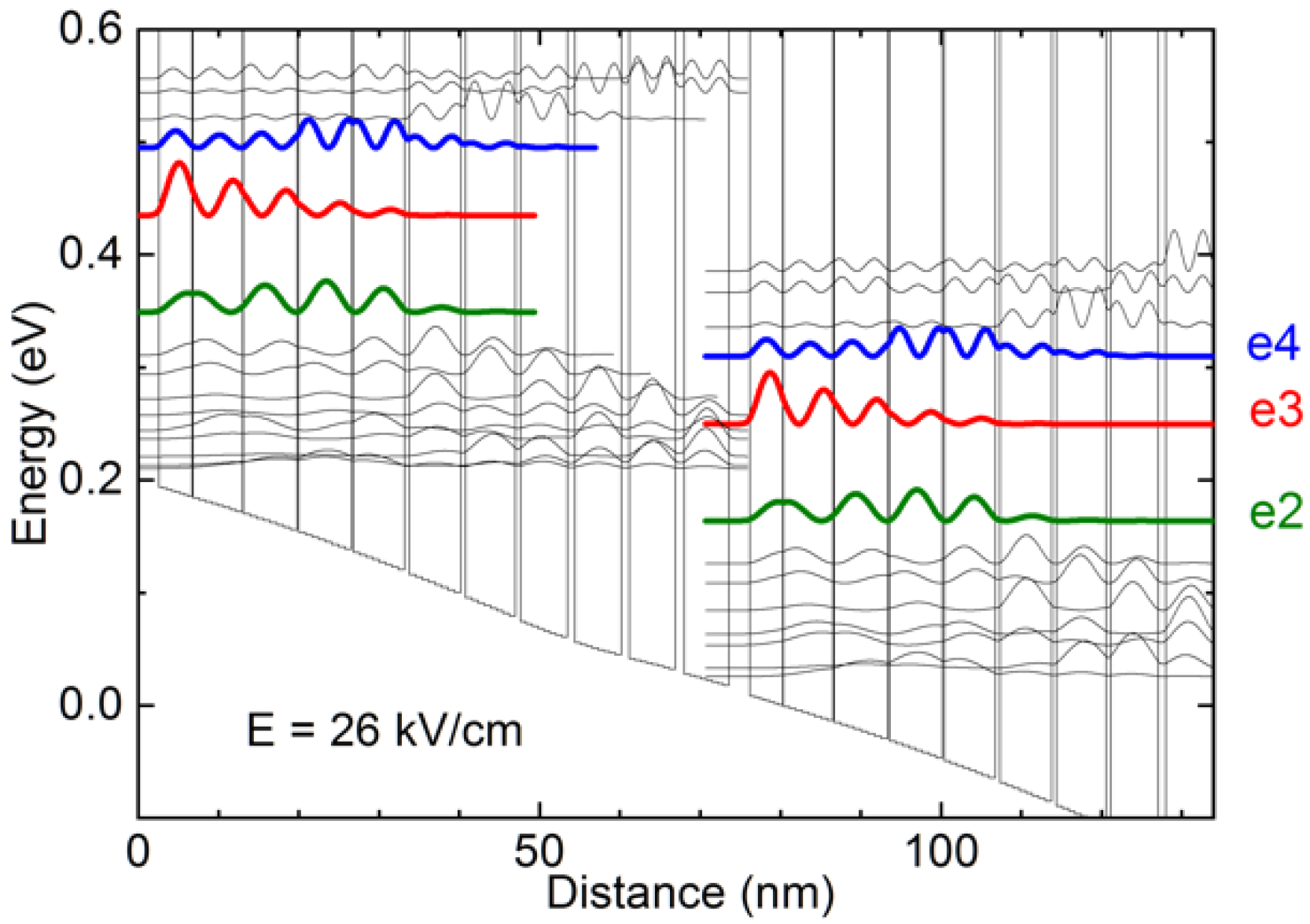
3] does not have enough flexibility to improve the separation of e3–e4 because an increase in the distance between the upper transition states is always accompanied by the same effect in the lower miniband of the structure, which deteriorates electron extraction from the lower transition level e2. In the new structure designed to emit near 14 µm (e3 − e2 = 88 meV) we added a thin quantum well after the injection barrier, which allowed us to increase the separation of e3–e4 to 65 meV at a bias corresponding to the expected threshold without a significant spread of lower levels. The width of the injector miniband at the threshold was moderately increased to Δ
inj = 141 meV from 105 meV in [
3]. Two quantum wells in the middle of the injector region were doped with Si at n = 8 × 10
16 cm
−3, whereas the thickness of the injection barrier in the new structure was increased from 2.1 to 2.6 nm to weaken the undesirable consequences of the higher doping. The larger injector miniband in the employed design, which is partially a consequence of the modification of the e3–e4 separation, limits additional thermal backfilling of the e2 level resulting from the increased doping (
Figure 1). The active zone of the QCL consists of 45 repetitions of the following layer sequence in Å and starting from the injection barrier:
26/41/
1/62/
1/67/
2/66/
2/64/
6/64/
6/62/
6/
59/
9/
58/
10/57/
11/56, where AlSb layers are in bold, and the Si-doped layers are underlined. The total electron sheet density
Ns in the structure, taking into account residual doping of InAs (n~5 × 10
15 cm
−3, estimated), is considered to be 1 × 10
11 cm
−2 per period. The active zone is separated from 3-µm-thick InAs cladding layers doped with Si to 7 × 10
17 cm
−3 by 3-µm-thick undoped InAs spacers. The overlap of the fundamental mode with the active region Γ and the waveguide loss for an empty waveguide
αw were calculated to be 0.5 and 3.6 cm
−1, respectively, using the COMSOL finite element solver. The Drude model was employed to find the waveguide loss associated with light absorption by free carriers in the doped cladding layers, no absorption in the QCL active zone was taken into account [
1]. The structure was grown by molecular beam epitaxy on an InAs substrate in a RIBER Compact 21 solid source machine equipped with valved cracker cells for the group V elements using growth rates of 0.33 and 0.5 mL/s for AlSb and InAs, respectively, and then processed into (7–20)-µm-wide ridge deep mesa devices using standard optical photolithography and wet chemical etching. Hard-baked photoresist was used for electrical insulation. The QCLs were soldered epi-side down on AlN heatsinks and placed for measurements into a liquid nitrogen flow cryostat.
The emission spectra of the lasers were measured using a Bruker V70 infrared Fourier transform spectrometer (FTIR) equipped with a pyroelectric detector. The emitted light was collected with an f/1 off-axis parabolic mirror, and another f/1 off-axis parabolic mirror was used to collimate the beam for optical power calibrations using a Melles Griot 13PEM001 power meter.
Fabricated QCLs with cleaved facets were tested in pulsed mode (330 ns/12 kHz). An additional 30 Hz current modulation was applied for pulsed measurements of light-current curves with the slow FTIR detector.
3. Results and Discussion
The threshold current density of the fabricated laser was lower than in previously reported InAs-based QCLs [
2,
3,
4,
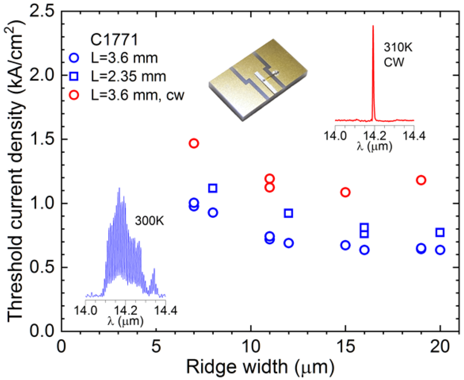
5]. In devices of 3.6 mm long, it ranged from 0.63 to 1.0 kA/cm
2 with the ridge width decreasing from 20 to 7 µm (
Figure 2).
Jth of some of these QCLs operated in the continuous wave regime is also shown in this plot as well as the pulsed data for 2.3-mm-long lasers. The best devices operated in cw mode up to 315–320 K. The increase in
Jth in narrow lasers is due to a larger overlap of the optical mode with absorbing dielectric on the mesa walls [
1]. The threshold current density was as low as 0.605 and 0.60 kA/cm
2 in 5- and 7.2-mm-long devices, respectively. The emission spectra of the lasers were centered between 14.0 and 14.3 µm at RT (inset in
Figure 2), close to the QCL gain peak position expected near the threshold (
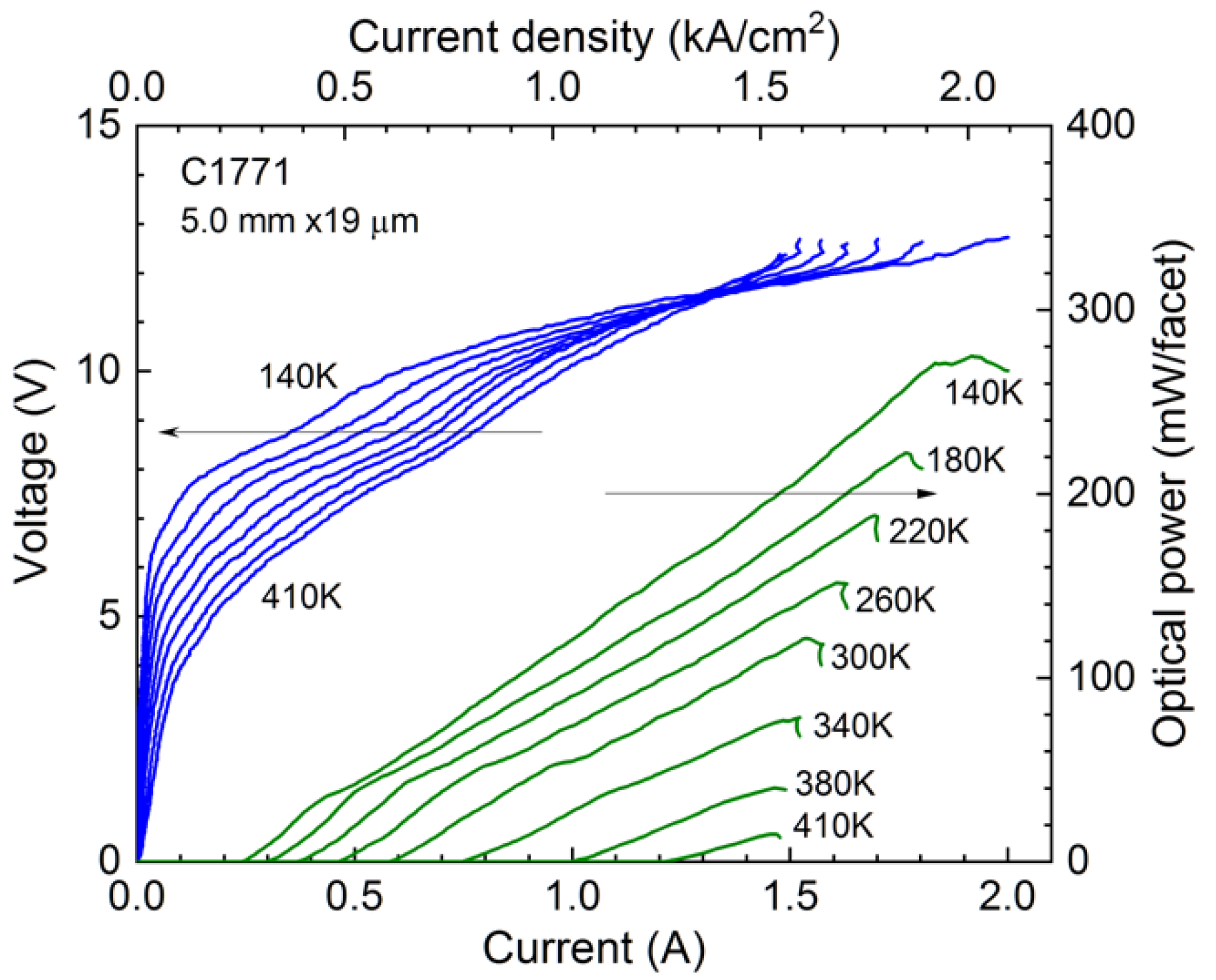
Figure 1). Typical voltage-current and light-current characteristics of the devices measured at different temperatures up to 410 K are shown in
Figure 3. The initial slope efficiency plotted as a function of temperature in
Figure 4 was also improved compared with the reference design [
3] from 80–90 to 90–110 mW/A or by about 20% in 3.6-mm-long lasers despite the smaller number of active stages, 45 instead of 55. The maximum pulsed optical power of 5-mm-long lasers reached 120 mW at RT with a slope efficiency of 130 mW/A (
Figure 3). The characteristic temperature of the threshold current temperature dependence
T0 increased up to 180 K from 165 K whereas the
T1 value, characterizing the reduction in the slope efficiency with temperature, increased from 260 to about 280 K in the tested devices (
Figure 4).
The threshold current densities demonstrated in this work are, to our knowledge, the lowest values ever reported for QCLs without facet treatment [
11]. The
Jth values obtained in the present work are 15–20% lower than in our InAs-based QCLs of the previous design [
3] and the output powers are higher to the same extent. Direct comparison of these results is complicated because the designs are quite different. The wafers were grown on different machines, and the influence of the growth conditions affecting the interface quality and residual doping is difficult to compare. We can however estimate to what extent the increased e3–e4 distance can be responsible for the observed improvements. For further analysis, we can use the general equation for the QCL threshold conditions, including the transparency current
Jtr [
15,
16]:
where
Jleak is the leakage current that can be attributed to parasitic recombination channels involving e4 (the effect of the states above e4 is neglected),
Jbf is the current corresponding to thermal backfilling of the lower transition level e2 [
14],
αm is the mirror loss depending on the laser length
L. The facet reflectivity
R calculated using the Fresnel formula yields
R = 0.29 for the given dielectric waveguide.
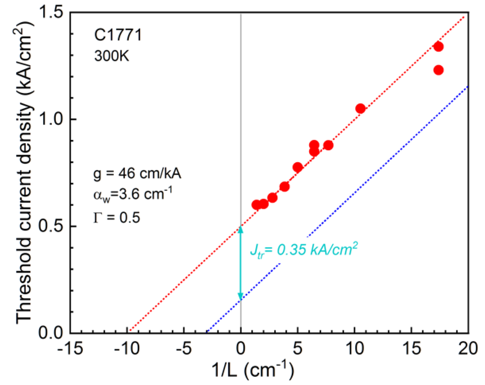
Figure 5 presents the threshold current density of the studied QCLs as a function of inverse resonator length.
With the calculated value of the optical confinement factor Γ = 0.5 we can find from these data the differential material gain
g = 46 cm/kA. The interception of the fitted straight line with the Y-axis gives a current that is the sum of the threshold current density
J0 in the absence of leakage and backfilling and
Jtr.
J0 = 0.15 kA/cm
2 and
Jtr = 0.35 kA/cm
2 can be found from these data using the extracted gain and the calculated waveguide loss
αw = 3.6 cm
−1. These data show that the transparency current is a major contribution to the QCL threshold at RT in long lasers. To estimate the impact of the increase in distance e3–e4 in the new design on the QCL threshold, we should first calculate
Jbf, which corresponds to the additional current through e3 required to compensate for a decrease in the population inversion due to electrons thermally excited to e2 from the ground injector states.
where
q is the electron charge, τ
3 is the lifetime in the upper transition level e3 and kT is the thermal energy [
17]. Assuming the calculated phonon lifetime τ
3 = 0.35 ps we can obtain an optimistic estimation for
Jbf = 0.16 kA/cm
2 and thus
Jleak = 0.19 kA/cm
2 in the considered structure. The leakage current is proportional to the electron concentration in e4 which in turn exponentially depends on the e3–e4 distance if we neglect the direct tunneling from the upper injector states [
15]. The increase of this parameter from 50 to 65 meV results in a 38% reduction in the e4 population and could thus provide a decrease of
Jleak from 0.31 kA/cm
2 to the observed value of 0.19 kA/cm
2 at RT. Consequently, the maximum improvement of
Jth due to the greater separation of the upper transition levels cannot exceed 0.12 kA/cm
2 in the studied structure, or 20% calculated as a ratio of
J0/
Jth at e3–e4 = 65 and 50 meV, that is, 0.15/0.5 and 0.15/(0.5 + 0.12). The differential quantum efficiency is proportional to
J0/
Jth [
14], so the maximum increase in output power can also be close to 20%. In the presence of interface recombination or other elastic scattering the thermal backfilling becomes more significant because of the shorter τ
3 and the part of
Jleak that can be affected by increasing the e3–e4 distance correspondingly drops. To summarize, the expansion of the e3–e4 separation in the new design is certainly useful for device operation but cannot provide a considerable performance improvement. It should be noted that in long-wavelength QCLs this distance approaches the lasing transition energy, and its further increase can result in absorption of the laser emission, which is illustrated in
Figure 6 displaying the gain spectrum of the studied QCL structure calculated using Nextnano NEGF software [
18] close to threshold. It is worth noting that Δ
inj increases with electric field, which will result in weaker backfilling in short lasers. Since
Jbf is the main component of threshold the
Jth(
1/
L), dependence should not be strictly linear. The data for long QCLs are more reliable to extract the differential gain.
For further performance improvement, it is necessary to reduce the thermal backfilling (Equation (2)). The injector miniband is already large in the used design, which can penalize continuous-wave operation because of the increased operating voltage. The doping level can be perhaps optimized in combination with the injection barrier thickness. The most important parameter responsible for the QCL performance is the electron lifetime in the upper transition level. An increased diagonality can be helpful to reduce the parasitic current associated with thermal backfilling. Note that the influence of interface scattering on the performance of the InAs-based QCLs is very strong because of the extremely high barriers in the InAs-based QCLs and the chemical nature of the InAs/AlSb interfaces, which limits the advantages of diagonal schemes. Novel designs with lower barriers in active quantum wells can be considered to moderate the effect of interface scattering.


