Communication

Theoretical Comparison of Optothermal Absorption in Transmissive Metalenses Composed of Nanobricks and Nanoholes

1
Research Center of Laser Fusion, China Academy of Engineering Physics, Mianyang 621900, China
2
Suzhou Institute of Nano-Tech and Nano-Bionics, Chinese Academy of Sciences, Suzhou 215125, China
3
Joint Laboratory for Extreme Conditions Matter Properties, Southwest University of Science and Technology, Mianyang 621010, China
*
Authors to whom correspondence should be addressed.
Photonics 2022, 9(1), 39; https://doi.org/10.3390/photonics9010039
Submission received: 10 November 2021 / Revised: 23 December 2021 / Accepted: 6 January 2022 / Published: 11 January 2022
(This article belongs to the Section Optoelectronics and Optical Materials)

Abstract

:
Background: Optical components with high damage thresholds are very desirable in intense-light systems. Metalenses, being composed of phase-control nanostructures with peculiar properties, are one of the important component candidates in future optical systems. However, the optothermal mechanism in metalenses is still not investigated adequately. Methods: In this study, the optothermal absorption in transmissive metalenses made of silicon nanobricks and nanoholes is investigated comparatively to address this issue. Results: The geometrical dependencies of nanostructures’ transmittance, phase difference, and field distribution are calculated numerically via simulations. To demonstrate the optothermal mechanism in metalenses, the mean absorption efficiencies of the selected unit-cells, which would constitute metalenses, are analyzed. The results show that the electric field in the silicon zone would lead to an obvious thermal effect, and the enhancement of the localized electric field also results in the strong absorption of optical energy. Then, two typical metalenses are designed based on these nanobricks and nanoholes. The optothermal simulations show that the nanobrick-based metalens can handle a power density of 0.15 W/µm2, and the density of the nanohole-based design is 0.12 W/µm2. Conclusions: The study analyzes and compares the optothermal absorption in nanobricks and nanoholes, which shows that the electric-field distribution in absorbent materials and the localized-field enhancement are the two key effects that lead to optothermal absorption. This study provides an approach to improve the anti-damage potentials of transmissive metalenses for intense-light systems.

1. Introduction

Intense-light systems increasingly impact laser fabrication [1], directed energy [2], renewable energy [3,4], etc. Transmissive phase components with high damage thresholds serve the crucial roles of beam shaping, steering, and focusing in these systems. Traditional refractive components mainly rely on geometrical shapes to bend rays, leading to the high complexity of intense-light systems. Flat optical components with anti-damage properties are the core to solving this problem. Particularly, metalenses, being composed of phase-control nanostructures with peculiar properties such as ultra-compact [5,6], large field of view [7,8], perfect absorption [9,10,11], etc., are one of the most important candidates for the future [12,13,14]. Many metasurfaces have been investigated to realize phase-control functions, such as imaging [15,16], steering [17,18,19], and holographic imaging [20,21]. However, the optothermal mechanism in metalenses is still not investigated adequately.
Due to the electromagnetic resonant effect, the electric field is usually localized in nanostructures [12], which would lead to optothermal absorption. This phenomenon is employed to induce deformation in laser fabrication of nanostructures [22]. The experiments show that the heat power volume density in nanostructures stems from the imaginary part of permittivity and the in situ electric field [23]. This optothermal effect is also experimentally demonstrated in other plasmonic [24] and dielectric [25,26] nanostructures. Thus, to improve damage thresholds, an intuitional method is to tune the electric field out of absorbent constituent materials, avoiding direct optothermal absorption. This method has been experimentally verified in anti-reflection nanotextures on fused silica, in which the strong electric field is tuned from nanostructures into the air and anti-damage properties are obtained successfully [27,28]. According to the method, our previous works also demonstrated that reflective metasurfaces made of dielectric nanoholes could be realized with high damage thresholds via field manipulation, and the electromagnetic mechanism has been explained via the electromagnetic distribution of excitation states [29,30]. To further demonstrate the principles of anti-damage metasurfaces, the optothermal mechanism in transmissive phase-control metalenses still requires investigation.
In this study, the optothermal absorption in transmissive phase-control metalenses made of silicon nanobricks and nanoholes are investigated comparatively. The optothermal absorption of the nanobricks and nanoholes with the 0-2π phase coverage is analyzed numerically. The results show that the electric field in the silicon zone would lead to an obvious thermal effect, and the enhancement of the localized electric field also results in strong absorption of optical energy. Then, two typical metalenses are constructed based on these nanostructures. The optothermal simulations show that the nanobrick-based metalens can handle a stronger laser of 0.15 W/µm2 than that (0.12 W/µm2) of nanoholes. The study demonstrates that the electric-field distribution in absorbent materials and the localized-field enhancement are the two key effects that lead to optothermal absorption, which improves the principles of designing anti-damage metalenses.

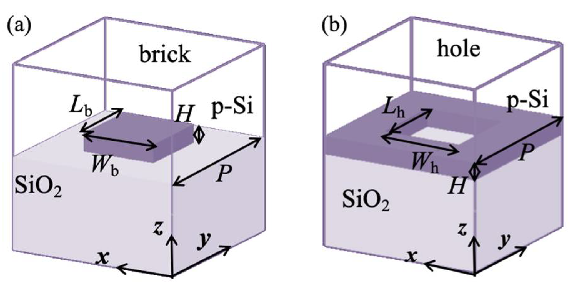
2. Materials and Methods

The studied transmissive metalenses are composed of periodic silicon (Si) nanobricks or nanoholes on SiO2 substrates with the same height H = 200 nm and the same lattice period P = 600 nm, as shown in Figure 1. Each unit-cell has a nanostructure with a rectangular shape described by length Lb or Lh, and width Wb or Wh. p-Si is chosen in the study due to its higher melting point and thermal stability than amorphous Si. The coating material is air, and the absorptivity could be ignorable. The incident light is continuous and polarized along the x-axis direction and injected from the bottom of the unit-cells. The wavelength is set as λ = 1064 nm, which is usually used in intense-light systems. The length and width are the control parameters used to manipulate the electric field distribution, phase difference, and transmittance.
For absorbent materials, the analytical model of the optothermal effect can be defined by the imaginary part of the complex permittivity ε of silicon and the in-situ electric field |E|, which can be described as [23]:
P a b s ( r , ω ) = 0.5 ε 0 ω | E ( r , ω ) | 2 i m a g ( ε ( r , ω ) ) s o u r c e p o w e r ( ω )
where P a b s ( r , ω ) is the spatial distribution of the fraction of absorbed power per cubic meter, normalized to the source power (unit: m−3). The absorption would transfer to heat, leading to the thermal effect. However, in metalenses made of nanostructures, the electric field distributes nonuniformly due to the localized-field effect. Subsequently, the simulation methods have to be exploited to calculate the electric field distribution in our study.
All the optical simulations in this study are implemented by the three-dimensional finite-difference time-domain (3D-FDTD) algorithm, and the optothermal simulations are based on the finite element method (FEM). The simulation region of nanostructures is surrounded by periodic boundaries in the x-axis and y-axis directions and perfectly matched layers in the z-axis direction. The simulation region of metalenses was surrounded by periodic boundaries in the y-axis direction and perfectly matched layers in the x-axis and z-axis directions. All the optical and thermal constants of materials were taken directly from the database [31].

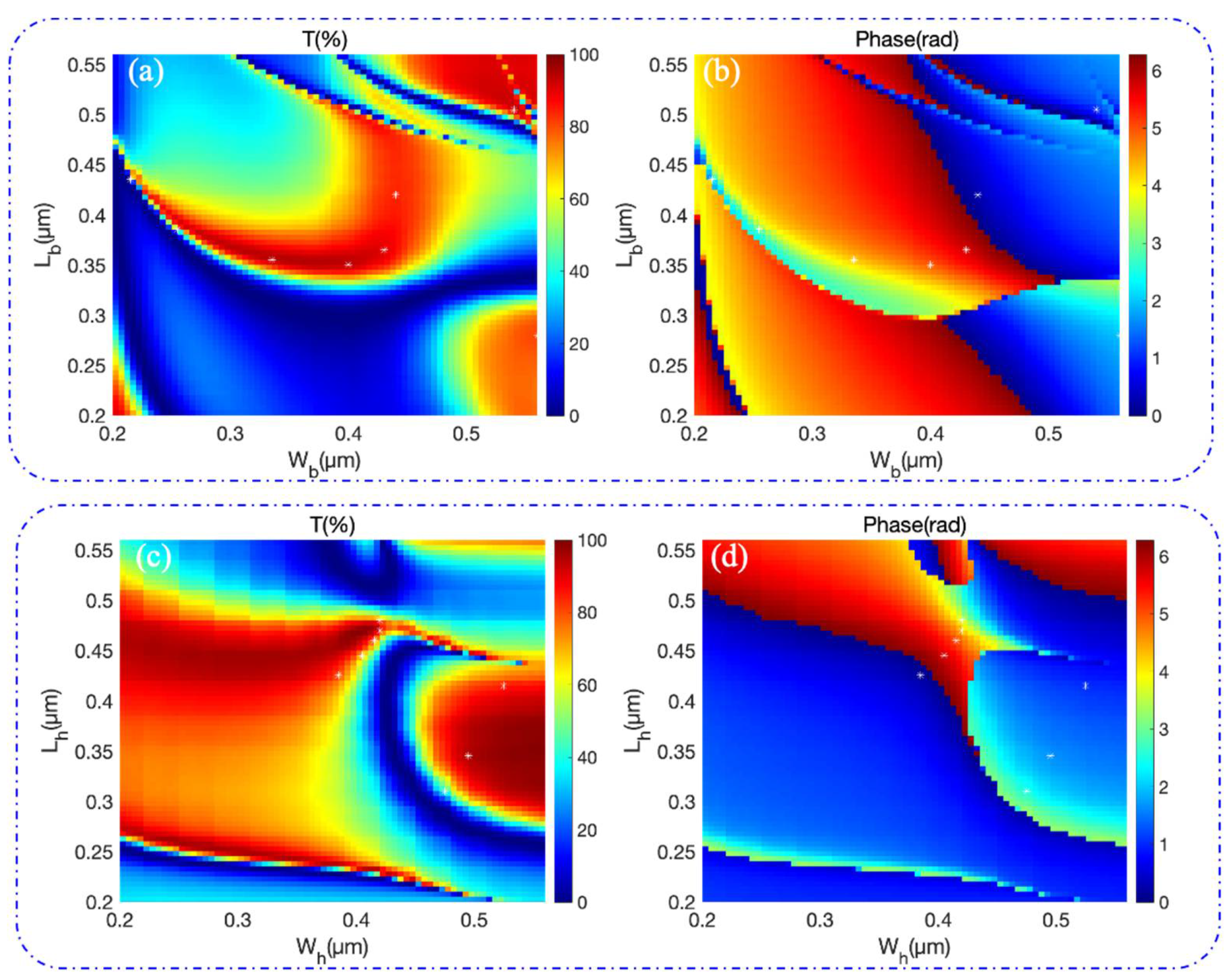
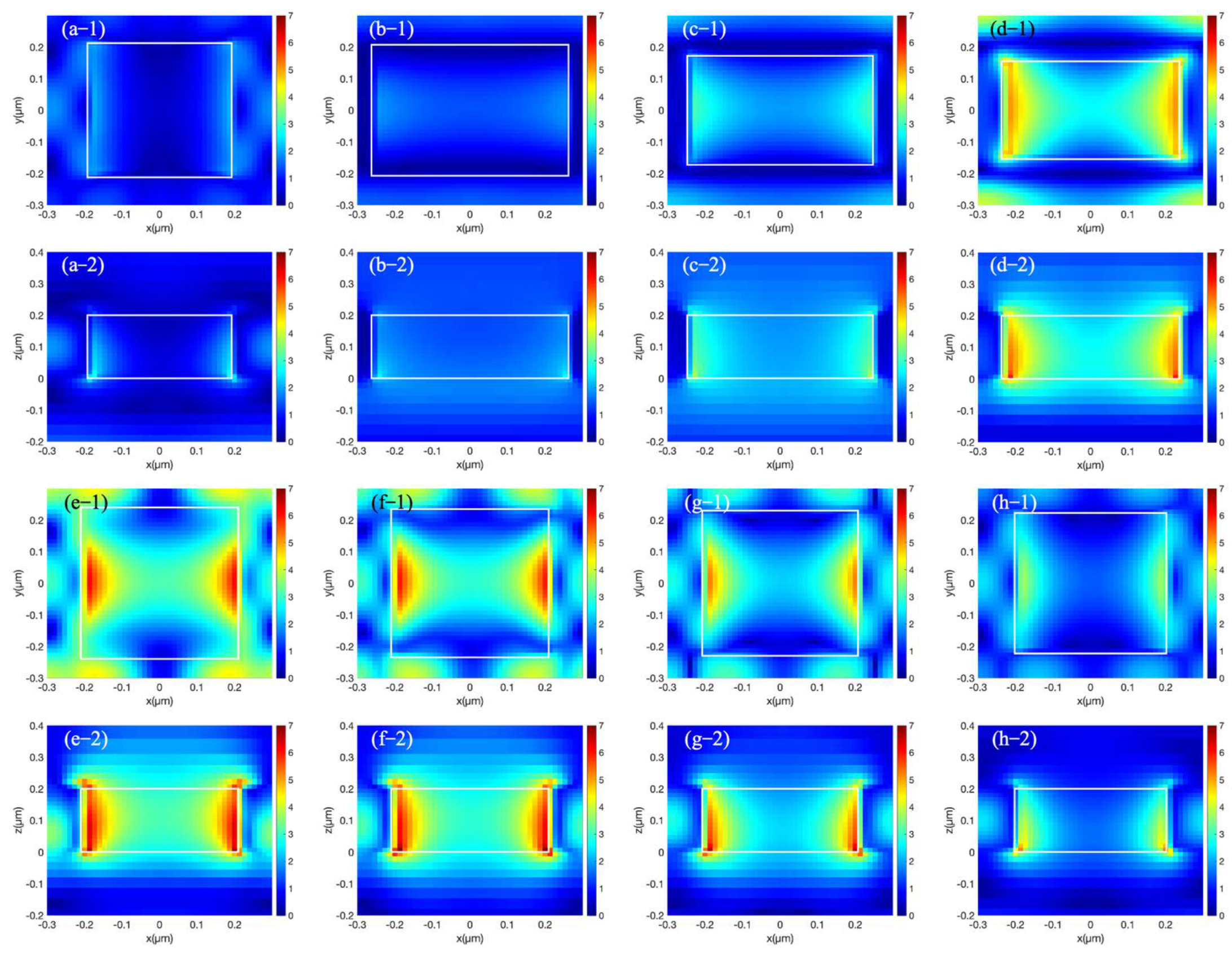
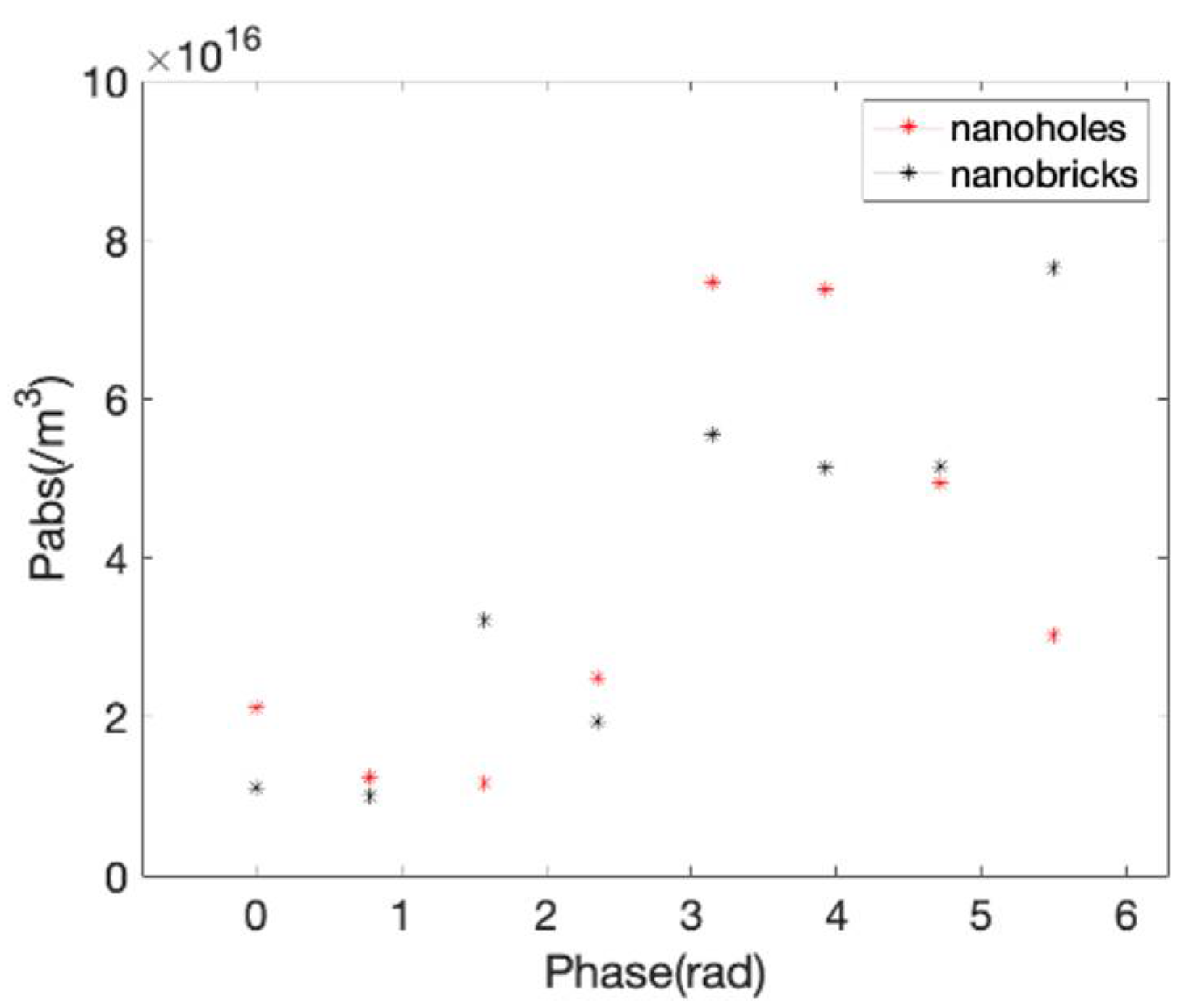
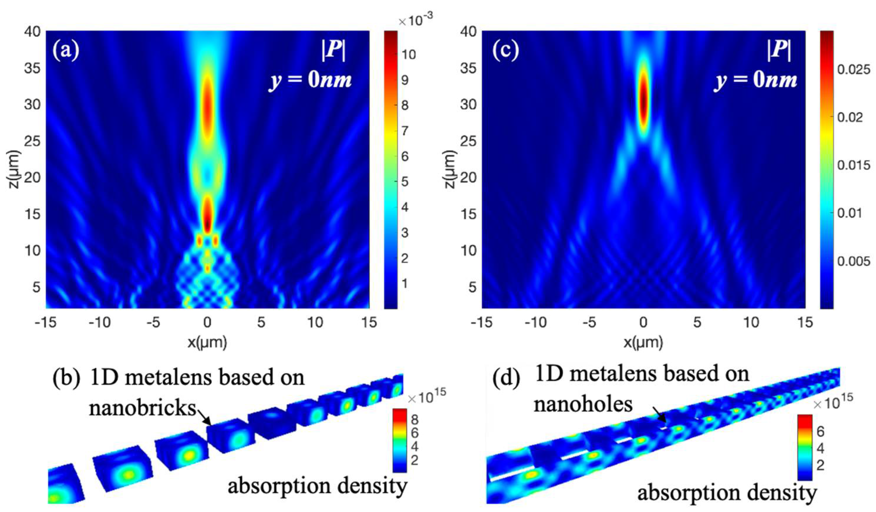
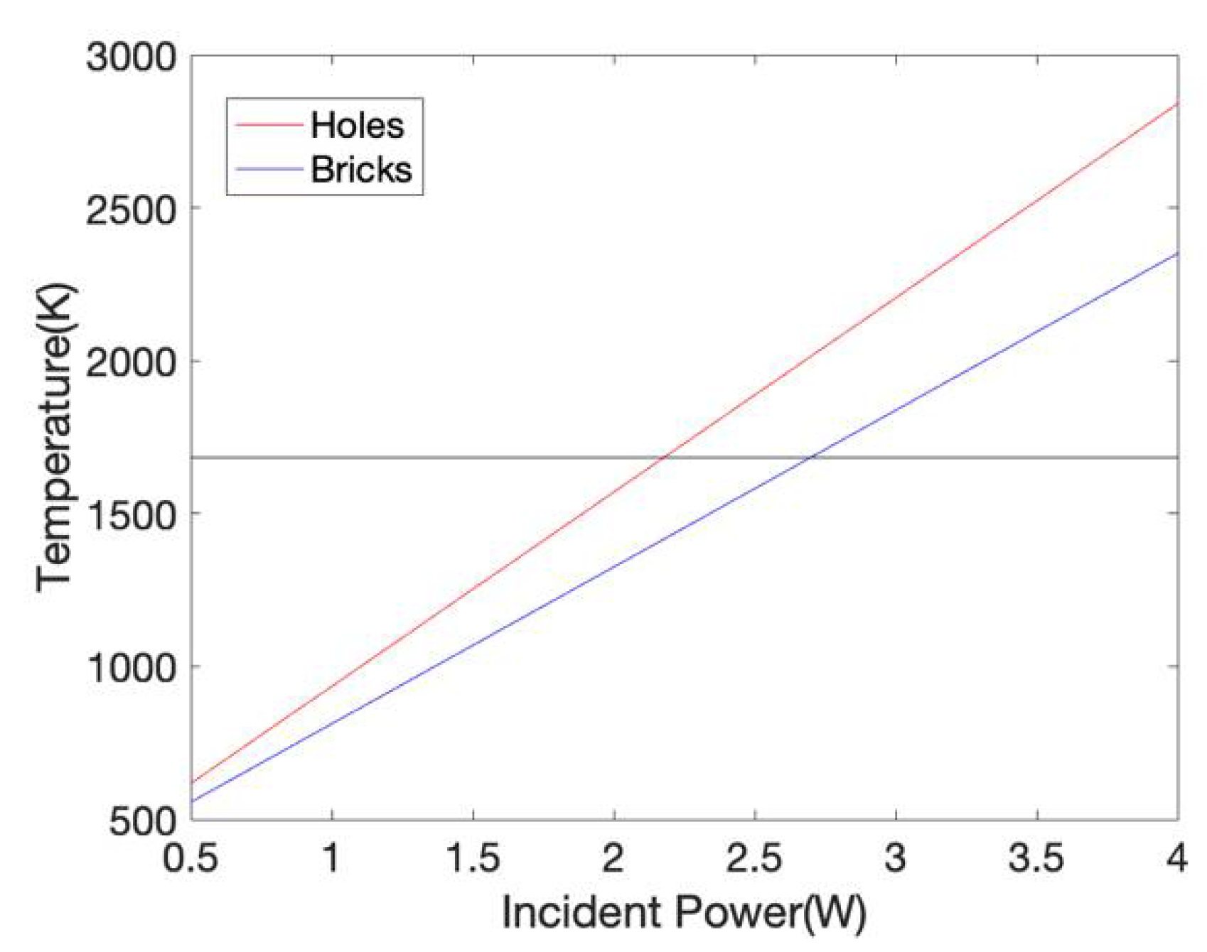
3. Results and Discussion

To construct transmissive metalenses, a group of unit-cells should be designed with high transmittance and phase differences covering the 0–2π range. By sweeping the parameters (length Lb and Lh, and width Wb and Wh) of the nanostructures, the geometrical dependencies of the transmittance and phase difference are obtained via calculating the S-matrix parameter of the unit-cells, as shown in Figure 2. When changing the width Wb and length Lb of nanobricks, the transmittance can be tuned as shown in Figure 2a, and the phase difference of a transmitted light changes as shown in Figure 2b. The transmittance and phase difference of the hole unit-cells are also the functions of Lh and Wh. The strips of high transmittance come from the coupling between the electric/magnetic dipoles in the nanostructures. With suitable geometrical parameters, high transmittance of more than 90% can be obtained. When tuning the nanostructures geometrically to obtain the 0-2π phase coverage, the transmittance of unit-cells will decrease. Except for the transmittance and phase coverage, the electric field distribution in the unit-cells is also important for the intense-light applications. Thus, the electric field distributions of these nanostructures are also obtained via simulations.
Metalenses are composed of nanostructures that have digitized phase-control values covering the 0–2π range. In this study, the 0–2π range is digitized by 8 phase points with an interval of π/4; thus eight unit-cells are selected. When selecting unit-cells, ±0.1 rad phase deviation is accepted to obtain better field confinement and higher transmittance, meaning that the unit-cells with phase differences of nπ/4 ± 0.1 rad (n = 0, 1, …, 8) are chosen first. Then, the unit-cells with in-air field confinement and high transmittance are selected, which are marked by the white stars in Figure 2. The details of the selected unit-cells are shown in Figure 3. The transmittance-phase relationship of nanobricks and nanoholes are shown in Figure 3a,b, while the others describe the widths and lengths of the selected nanostructures. It is noted that at the phase point of 3π/4, the transmittance is only 50%. The most energy is reflected by the nanostructure, not absorbed.
The responding electric field distributions of the selected unit-cells are shown in Figure 4 and Figure 5 for nanobricks and nanoholes, respectively. The electric field of the selected unit-cells is normalized with the source. The x–y–plane distributions of field |E| are obtained with z = 100 nm, while the x–z–plane distributions are obtained with y = 0 nm. Because the phase control of transmitted light relies on the electromagnetic resonances, the field-enhancement effect in some unit-cells is inevitable to obtain the 0–2π phase coverage. To demonstrate the influence of the field distribution on the optothermal absorption, the optothermal absorption efficiencies of the selected unit-cells are simulated, and the mean values are shown in Figure 6. Under the illumination of the continuous incident light, the partial heat would spread rapidly to the whole nanostructure by thermal transmission due to the subwavelength size. Thus, the mean absorption is considered here. In Figure 4 and Figure 5, for both nanobricks and nanoholes, the absorption efficiencies at the phase points (0, π/4, π/2, 3π/4) are smaller than the others. In Figure 4, we can see that at the phase points (π, 5π/4, 3π/2, 7π/4), these unit-cells have stronger electric resonances and localized field intensities in the silicon bricks than that in the air zone. It means that the electric field in absorbent materials would lead to strong optothermal, and tuning the field into the air zone with ignorable absorption can reduce the heat effect. For example, in Figure 4b,c, the very strong field appears in the air zone, leading to a low absorption in Figure 6. These electric fields do not interact with the silicon directly, avoiding the optothermal effect. On the other hand, in Figure 5e–h, although most fields of nanoholes distribute in the air holes, some points with strong field intensities enhanced by the nanostructures appear on the Si–SiO2 interfaces, resulting in strong absorption. Absorption is related to the square of the electric field amplitude |E2|; thus, the field enhancement in absorbent materials will result in a strong absorption.
Based on the selected unit-cells with the 0–2π coverage in Figure 3, two 1D metalenses are constructed and investigated. The phase profiles of the metalenses are φ ( x ) = k 0 ( x 2 + f 2 f ) , where k 0 is the wavenumber in a vacuum, x is the x-axis coordinate, and f is the focal length. The simulated metalenses have the size of 30 µm (x-axis) × 0.6 µm (y-axis). The focusing performances of the two metalenses are shown in Figure 7a,c. In optical absorption simulations, the x-axis and y-axis boundaries of the metalenses are set as “closed”, and the z-axis boundaries are set as “shell”. The absorption density distributions Pabs are shown in Figure 7c,d. It is seen that the absorption mainly concentrates in the nanobricks or at the corners of the nanoholes. Due to the heat conduction, the temperature distribution is different from the absorption density distribution. Thermal damage would appear once the maximum temperature in metalens is higher than the melting point 1683 K of silicon. Under the illumination of different incident power, the maximum temperature values in the metalenses are simulated via the finite element method, as shown in Figure 8. To remove the influence of the environment, the ambient temperature of the SiO2 substrate and air is set as a constant value of 300 K. In the heat simulations, all boundaries of the metalenses are set as “closed”. When the illumination power changes, the corresponding heat energy will vary according to the absorption efficiencies in Figure 7. After calculating the thermal conduction and convection of the heat energy, it will stay at a steady-state. Then, the temperature distributions of the metalenses with varying illumination power are obtained. With the assumption that the optothermal property of silicon remains unchanged before the thermal damage happens, the maximum temperature has a linear relationship with the incident power. Although the stronger field distributes in the air zone, some weaker field still stays in the silicon and would be absorbed via the optothermal conversion, as shown in Figure 7b,d. Under the illumination of continuous light with a high power-density, the highest temperatures of metalenses can reach the metaling point due to heat accumulation. The metalens made of nanobricks starts to be damaged with an indent power of 2.70 W, while the nanohole one can handle the highest power of 2.18 W. The corresponding maximum power-density values are 0.15 W/µm2 and 0.12 W/µm2, respectively.

4. Conclusions

In this study, the optothermal absorption in transmissive metalenses made of silicon nanobricks and nanoholes was investigated comparatively. The transmittance, phase difference, and field distribution of nanobricks and nanoholes were numerically analyzed. The optothermal results show that the electric field in the silicon zone would lead to an obvious thermal effect. The in-air electric field would not be absorbed by absorbent materials, avoiding the optothermal conversion. Meanwhile, the field enhancement also results in strong absorption of optical energy. Thus, the key to designing anti-damage metalens is manipulating the field distribution out of absorbent materials and restraining the field enhancement in nanostructures. Two presentative metalenses were designed based on these nanobricks and nanoholes. The optothermal simulations show that they can handle a maximum laser density of 0.15 W/µm2 and 0.12 W/µm2. The study compared the optothermal conversion in transmissive metalenses, demonstrating the two key optothermal factors of electric-field distribution and enhancement. This provided an approach to improving high damage thresholds in transmissive metalenses for intense-light systems.

Author Contributions

Conceptualization, X.Y.; methodology, F.T.; software, Q.L.; investigation, F.T.; resources, H.Y. and X.Y.; writing—original draft preparation, F.T.; writing—review and editing, F.T. and Q.L.; supervision, H.Y.; funding acquisition, H.Y., Z.Y. and X.Y. All authors have read and agreed to the published version of the manuscript.

Funding

This research was funded by the National Natural Science Foundation of China, grant number [61705204, 61705206]; Innovation and Development Foundation of China Academy of Engineering Physics, grant number [CX20200021]; Natural Science Foundation of Jiangsu Province, grant number [BK20190229]; Scientific Research Fund of Sichuan Provincial Science and Technology Department, grant number [2020YJ0137].

Conflicts of Interest

The authors declare no conflict of interest.

References

  1. Xie, X.; Weng, Q.; Luo, Z.; Long, J.; Wei, X. Thermal performance of the flat micro-heat pipe with the wettability gradient surface by laser fabrication. Int. J. Heat Mass Transf. 2018, 125, 658–669. [Google Scholar] [CrossRef]
  2. Wang, Z.; Palmer, T.A.; Beese, A. Effect of processing parameters on microstructure and tensile properties of austenitic stainless steel 304L made by directed energy deposition additive manufacturing. Acta Mater. 2016, 110, 226–235. [Google Scholar] [CrossRef] [Green Version]
  3. Miquel, J.-L.; Lion, C.; Vivini, P. The Laser Mega-Joule: LMJ & PETAL status and Program Overview. J. Phys. Conf. Ser. 2016, 688, 012067. [Google Scholar] [CrossRef]
  4. Moses, E.I.; Lindl, J.D.; Spaeth, M.L.; Patterson, R.W.; Sawicki, R.H.; Atherton, L.J.; Baisden, P.A.; Lagin, L.J.; Larson, D.W.; MacGowan, B.J.; et al. Overview: Development of the National Ignition Facility and the Transition to a User Facility for the Ignition Campaign and High Energy Density Scientific Research. Fusion Sci. Technol. 2016, 69, 1–24. [Google Scholar] [CrossRef]
  5. Faraji-Dana, M.; Arbabi, E.; Arbabi, A.; Kamali, S.M.; Kwon, H.; Faraon, A. Compact folded metasurface spectrometer. Nat. Commun. 2018, 9, 1–8. [Google Scholar] [CrossRef]
  6. Li, Z.; Tang, F.; Shang, S.; Wu, J.; Shao, J.; Liao, W.; Kong, B.; Zeng, T.; Ye, X.; Jiang, X.; et al. Compact metalens-based integrated imaging devices for near-infrared microscopy. Opt. Express 2021, 29, 27041. [Google Scholar] [CrossRef] [PubMed]
  7. Paniagua-Domínguez, R.; Yu, Y.F.; Khaidarov, E.; Choi, S.; Leong, V.; Bakker, R.M.; Liang, X.; Fu, Y.H.; Valuckas, V.; Krivitsky, L.A.; et al. A Metalens with a Near-Unity Numerical Aperture. Nano Lett. 2018, 18, 2124–2132. [Google Scholar] [CrossRef] [Green Version]
  8. Pu, M.; Li, X.; Guo, Y.; Ma, X.; Luo, X. Nanoapertures with ordered rotations: Symmetry transformation and wide-angle flat lensing. Opt. Express 2017, 25, 31471–31477. [Google Scholar] [CrossRef]
  9. Chen, X.; Zhou, Y.; Han, H.; Wang, X.; Zhou, L.; Yi, Z.; Fu, Z.; Wu, X.; Li, G.; Zeng, L. Optical and magnetic properties of small-size core–shell Fe3O4@C nanoparticles. Mater. Today Chem. 2021, 22, 100556. [Google Scholar] [CrossRef]
  10. Zhou, F.; Qin, F.; Yi, Z.; Yao, W.-T.; Liu, Z.; Wu, X.; Wu, P. Ultra-wideband and wide-angle perfect solar energy absorber based on Ti nanorings surface plasmon resonance. Phys. Chem. Chem. Phys. 2021, 23, 17041–17048. [Google Scholar] [CrossRef]
  11. Wu, X.; Zheng, Y.; Luo, Y.; Zhang, J.; Yi, Z.; Wu, X.; Cheng, S.; Yang, W.; Yu, Y.; Wu, P. A four-band and polarization-independent BDS-based tunable absorber with high refractive index sensitivity. Phys. Chem. Chem. Phys. 2021, 23, 26864–26873. [Google Scholar] [CrossRef]
  12. Hsiao, H.-H.; Chu, C.H.; Tsai, D.P. Fundamentals and Applications of Metasurfaces. Small Methods 2017, 1, 1600064. [Google Scholar] [CrossRef] [Green Version]
  13. Li, N.; Xu, Z.; Dong, Y.; Hu, T.; Zhong, Q.; Fu, Y.H.; Zhu, S.; Singh, N. Large-area metasurface on CMOS-compatible fabrication platform: Driving flat optics from lab to fab. Nanophotonics 2020, 9, 3071–3087. [Google Scholar] [CrossRef]
  14. Hou-Tong, C.; Antoinette, J.T.; Nanfang, Y. A review of metasurfaces: Physics and applications. Rep. Prog. Phys. 2016, 79, 076401. [Google Scholar]
  15. Lin, R.J.; Su, V.-C.; Wang, S.; Chen, M.K.; Chung, T.L.; Chen, Y.H.; Kuo, H.Y.; Chen, J.-W.; Chen, J.; Huang, Y.-T.; et al. Achromatic metalens array for full-colour light-field imaging. Nat. Nanotechnol. 2019, 14, 227–231. [Google Scholar] [CrossRef]
  16. Wang, S.; Lai, J.; Wu, T.; Chen, C.; Sun, J. Wide-band achromatic flat focusing lens based on all-dielectric subwavelength metasurface. Opt. Express 2017, 25, 7121–7130. [Google Scholar] [CrossRef] [PubMed]
  17. Yu, Y.F.; Zhu, A.Y.; Paniagua-Dominguez, R.; Fu, Y.H.; Luk’Yanchuk, B.; Kuznetsov, A.I. High-transmission dielectric metasurface with 2π phase control at visible wavelengths. Laser Photon Rev. 2015, 9, 412–418. [Google Scholar] [CrossRef]
  18. Shalaev, M.I.; Sun, J.; Tsukernik, A.; Pandey, A.; Nikolskiy, K.; Litchinitser, N.M. High-Efficiency All-Dielectric Metasurfaces for Ultracompact Beam Manipulation in Transmission Mode. Nano Lett. 2015, 15, 6261–6266. [Google Scholar] [CrossRef] [PubMed] [Green Version]
  19. Liu, L.; Zhang, X.; Kenney, M.; Su, X.; Xu, N.; Ouyang, C.; Shi, Y.; Han, J.; Zhang, W.; Zhang, S. Broadband Metasurfaces with Simultaneous Control of Phase and Amplitude. Adv. Mater. 2014, 26, 5031–5036. [Google Scholar] [CrossRef]
  20. Hu, Y.; Luo, X.; Chen, Y.; Liu, Q.; Li, X.; Wang, Y.; Liu, N.; Duan, H. 3D-Integrated metasurfaces for full-colour holography. Light. Sci. Appl. 2019, 8, 1–9. [Google Scholar] [CrossRef]
  21. Lingling, H.; Shuang, Z.; Thomas, Z. Metasurface holography: From fundamentals to applications. Nanophotonics 2018, 7, 1169–1190. [Google Scholar]
  22. Berzinš, J.; Indrišiūnas, S.; Fasold, S.; Steinert, M.; Žukovskaja, O.; Cialla-May, D.; Gečys, P.; Bäumer, S.M.B.; Pertsch, T.; Setzpfandt, F. Laser-induced spatially-selective tailoring of high-index dielectric metasurfaces. Opt. Express 2020, 28, 1539–1553. [Google Scholar] [CrossRef]
  23. Chen, X.; Chen, Y.; Yan, M.; Qiu, M. Nanosecond Photothermal Effects in Plasmonic Nanostructures. ACS Nano 2012, 6, 2550–2557. [Google Scholar] [CrossRef]
  24. Zhang, Y.; Shi, L.; Hu, D.; Chen, S.; Xie, S.; Lu, Y.; Cao, Y.; Zhu, Z.; Jin, L.; Guan, B.-O.; et al. Full-visible multifunctional aluminium metasurfaces by in situ anisotropic thermoplasmonic laser printing. Nanoscale Horiz. 2019, 4, 601–609. [Google Scholar] [CrossRef]
  25. Zhu, X.; Yan, W.; Levy, U.; Mortensen, N.A.; Kristensen, A. Resonant laser printing of structural colors on high-index dielectric metasurfaces. Sci. Adv. 2017, 3, e1602487. [Google Scholar] [CrossRef] [Green Version]
  26. Aouassa, M.; Mitsai, E.; Syubaev, S.; Pavlov, D.; Zhizhchenko, A.; Jadli, I.; Hassayoun, L.; Zograf, G.; Makarov, S.; Kuchmizhak, A. Temperature-feedback direct laser reshaping of silicon nanostructures. Appl. Phys. Lett. 2017, 111, 243103. [Google Scholar] [CrossRef]
  27. Ye, X.; Hu, X.; Tang, F.; Wu, J.; Yang, L.; Huang, J.; Zheng, W. Laser field manipulation and laser damage resistance property of nanotextures on fused silica optics. Results Phys. 2020, 18, 103262. [Google Scholar] [CrossRef]
  28. Jing, X.; Tian, Y.; Han, J.; Ma, J.; Jin, Y.; Shao, J.; Fan, Z. Polarization effect of femtosecond pulse breakdown in subwavelength antireflective relief grating. Opt. Commun. 2011, 284, 4220–4224. [Google Scholar] [CrossRef]
  29. Yu, H.; Tang, F.; Chen, J.; Yi, Z.; Ye, X.; Wang, Y. Reflective Meta-Films with Anti-Damage Property via Field Distribution Manipulation. Coatings 2021, 11, 640. [Google Scholar] [CrossRef]
  30. Yu, H.; Tang, F.; Wu, J.; Yi, Z.; Ye, X.; Wang, Y. Meta-Deflectors Made of Dielectric Nanohole Arrays with Anti-Damage Potential. Photonics 2021, 8, 107. [Google Scholar] [CrossRef]
  31. Palik, E.D. Handbook of Optical Constants of Solids; Academic Press: Cambridge, MA, USA, 1998; Volume 3. [Google Scholar]
Figure 1. Schematics of two unit-cells: (a) Nanobricks; (b) Nanoholes. The nanostructures have the same parameters as height H = 200 nm and lattice period P = 600 nm. The rectangular shapes are described by length Lb and Lh, and width Wb and Wh, respectively.
Photonics 09 00039 g001
Figure 2. Optical properties of the unit-cells with nanobricks and nanoholes: (a) Transmittance and (b) Phase difference of the brick unit-cells as a function of Lb and Wb; (c) Transmittance and (d) Phase difference of the hole unit-cells as a function of Lh and Wh.
Photonics 09 00039 g002
Figure 3. The eight unit-cells with nanobricks or nanoholes selected for constructing metalenses: The transmittance and phase difference of (a) Nanobricks and (b) Nanoholes. The widths and lengths of (c) Nanobricks and (d) Nanoholes.
Photonics 09 00039 g003
Figure 4. Electric field distributions of the eight selected unit-cells with nanobricks: (a1h1) Normalized electric field distribution on the x−y plane with z = 100 nm; (a2h2) Normalized electric field distribution on the x−z plane with y = 0 nm.
Photonics 09 00039 g004
Figure 5. Electric field distributions of the eight selected unit-cells with nanoholes: (a1h1) Normalized electric field distribution on the x−y plane with z = 100 nm; (a2h2) Normalized electric field distribution on the x−z plane with y = 0 nm.
Photonics 09 00039 g005
Figure 6. The mean absorption efficiencies of the selected unit-cells, which are defined as absorbed power per cubic meter, normalized to the source power.
Photonics 09 00039 g006
Figure 7. Focusing and absorption of the metalenses: (a) Intensity distribution at the focal point of the brick metalens; (b) The absorption density distribution in the brick metalens; (c) Intensity distribution at the focal point of the hole metalens; (d) The absorption density distribution in the hole metalens.
Photonics 09 00039 g007
Figure 8. The maximum temperature in the metalenses with a nanobrick (blue) or nanohole (red) configuration under the illumination of different incident power. The black line marks the melting point of 1683 K of silicon.
Photonics 09 00039 g008
Publisher’s Note: MDPI stays neutral with regard to jurisdictional claims in published maps and institutional affiliations.

