Communication

Electrical Characterizations of 35-kV Semi-Insulating Gallium Arsenide Photoconductive Switch

Key Laboratory of Ultrafast Photoelectric Technology and Terahertz Science in Shaanxi, Xi’an University of Technology, Xi’an 710048, China
*
Author to whom correspondence should be addressed.
Photonics 2021, 8(9), 385; https://doi.org/10.3390/photonics8090385
Submission received: 2 August 2021 / Revised: 7 September 2021 / Accepted: 7 September 2021 / Published: 10 September 2021

Abstract

:
In this paper, a three-layer GaAs photoconductive semiconductor switch (GaAs PCSS) is designed to withstand high voltage from 20 to 35 kV. The maximum avalanche gain and minimum on-state resistance of GaAs PCSS are 1385 and 0.58 Ω, respectively, which are the highest values reported to date. Finally, the influence of the bias voltage on the avalanche stability is analyzed. The stability of the GaAs PCSS is evaluated and calculated. The results show that the jitter values at the bias voltages of 30 kV and 35 kV are 164.3 ps and 106.9 ps, respectively. This work provides guidance for the design of semiconductor switches with high voltage and high gain.

Graphical Abstract

1. Introduction

High-power nanosecond ultrafast switching devices have been widely used in high-power microwave systems, mostly as trigger generators in the Z-pinch pulsed-power systems. They have also been used in the biomedical industry [1,2,3,4,5,6,7,8,9,10]. A photoconductive semiconductor switch (PCSS) can operate at high voltage, has a low inductance, and can provide a high-speed response to laser pulses. These properties make the PCSS a suitable solution for both ultra-high-speed electronic applications and high-power pulse generation [11,12,13,14,15,16].
Silicon carbide (SiC) material is a single energy valley structure; there is no electron transfer effect, therefore the SiC switch can work only in linear mode [17,18,19,20,21,22]. Unlike silicon carbide (SiC) PCSS, the gallium arsenide (GaAs) PCSS can also operate in the high multiplier mode. Therefore, it has been suitable for usage in accelerators, which require PCSS operation at the bias voltage level of above 30 kV. However, under such a high bias voltage, surface flashover can occur at the PCSS surface, which can damage the switch. This phenomenon is caused by a high bias voltage, and it reduces the lifetime of a GaAs PCSS and restricts its usage in high-voltage applications [23,24]. In recent years, the advances concerning the voltage endurance level have remained limited, making it an interesting research area. In this paper, a high avalanche gain GaAs PCSS is designed and manufactured to obtain high avalanche gain at a high bias voltage by optimizing the electrode and insulating the switch surface.

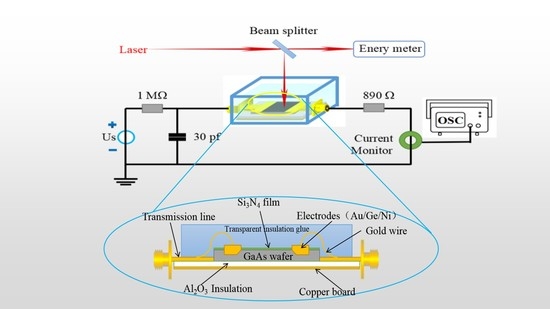
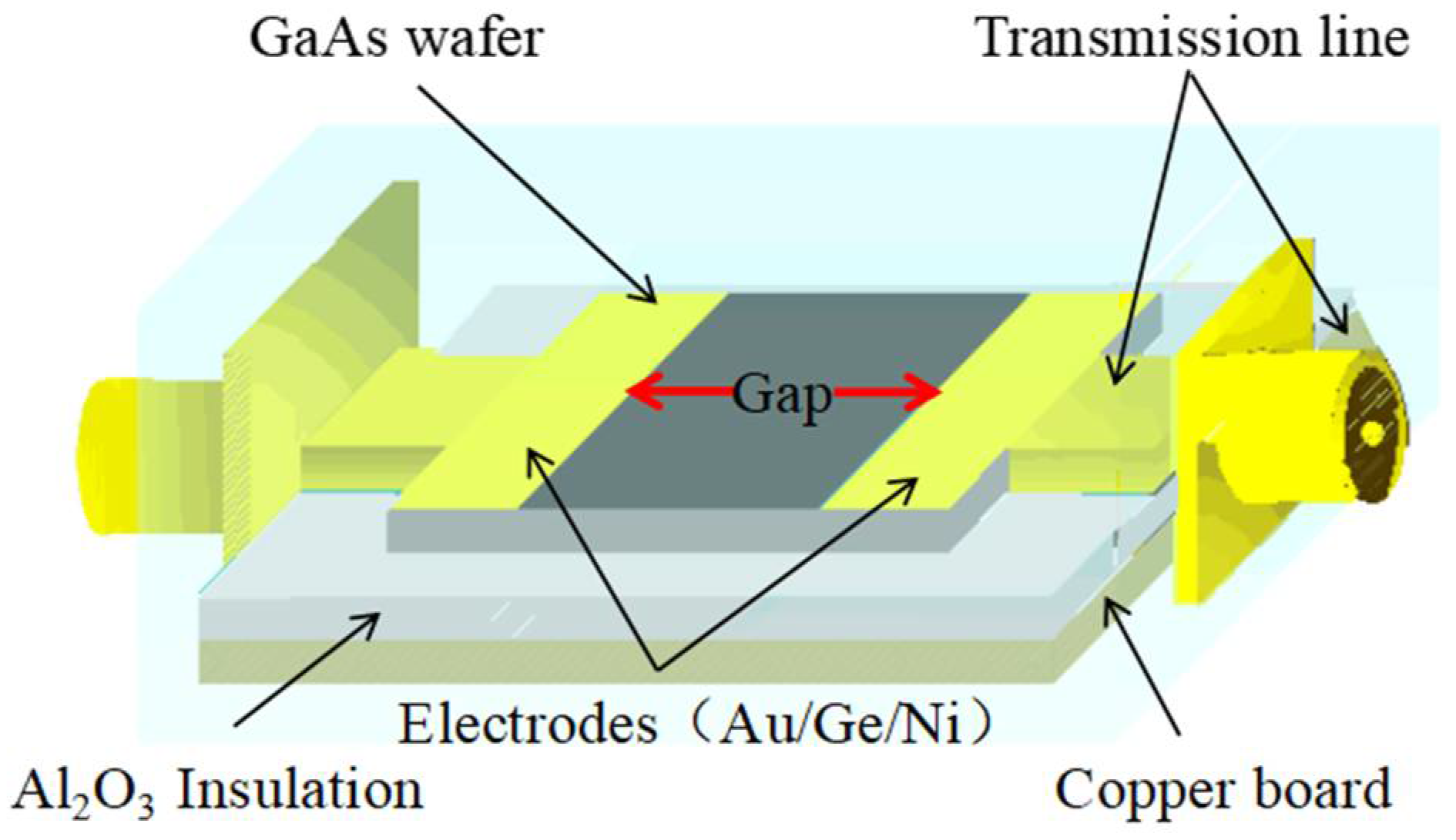
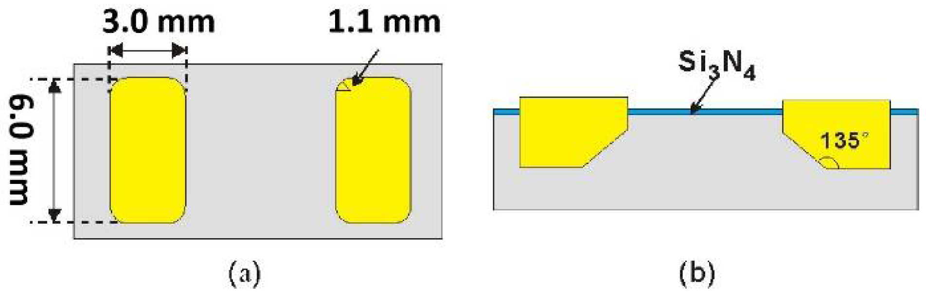
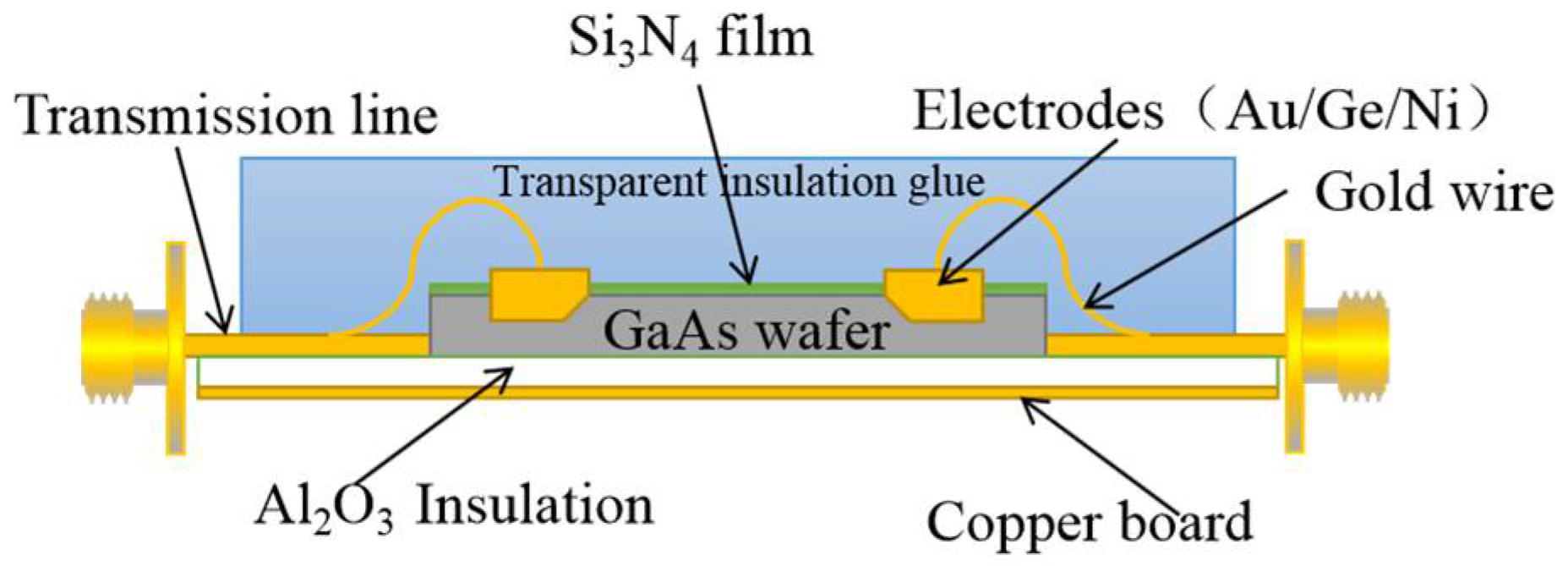
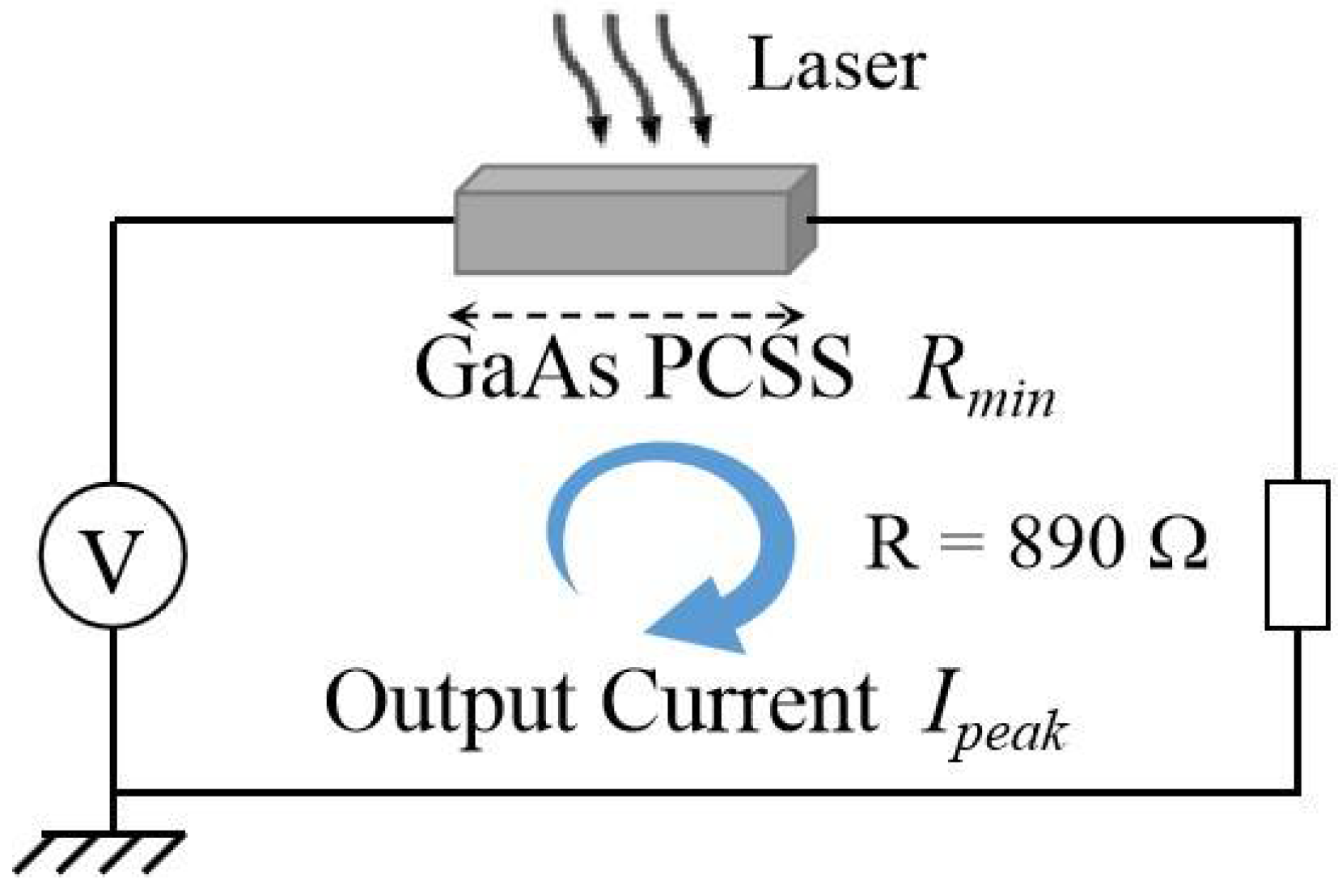
2. Materials and Methods
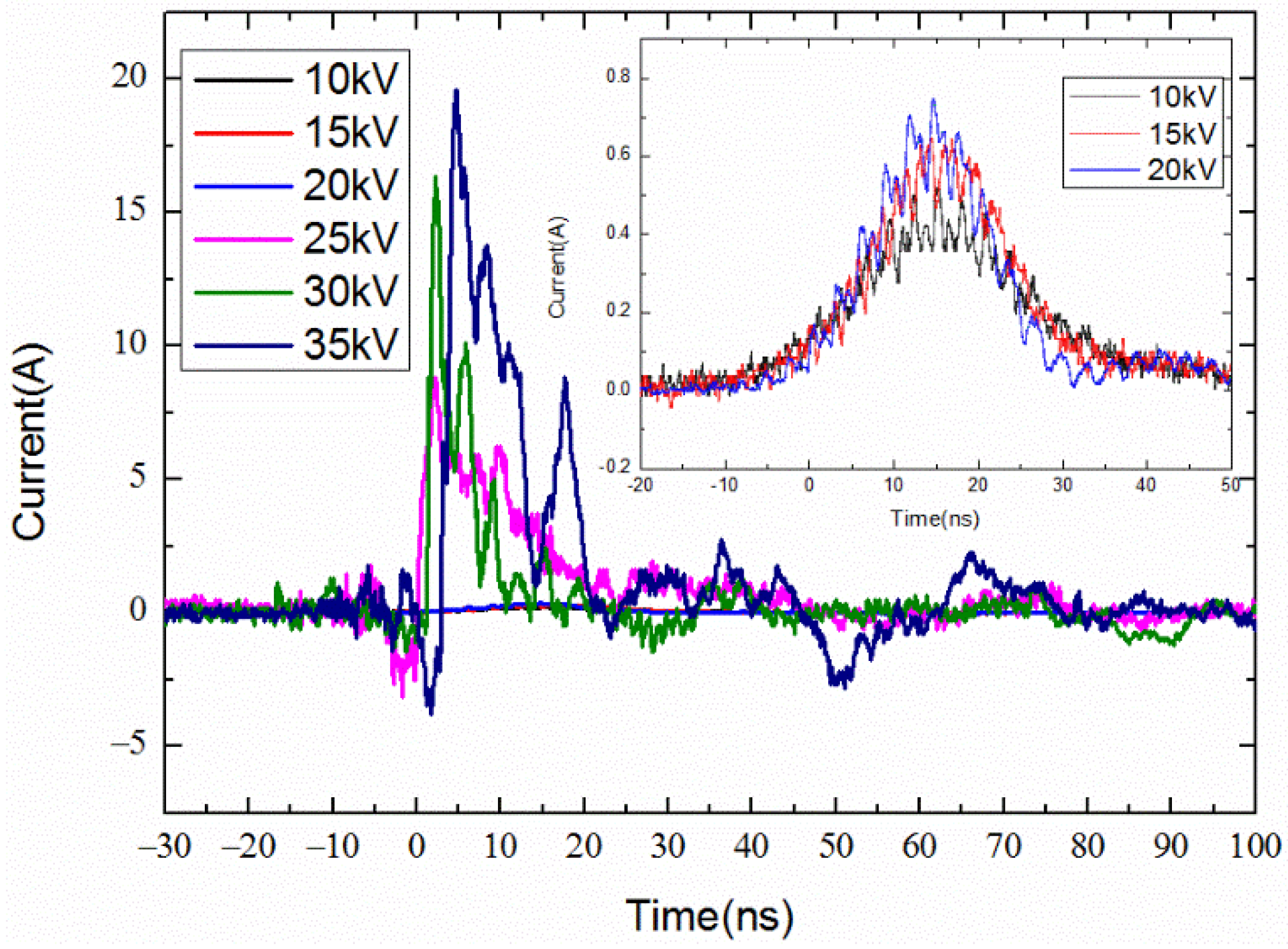
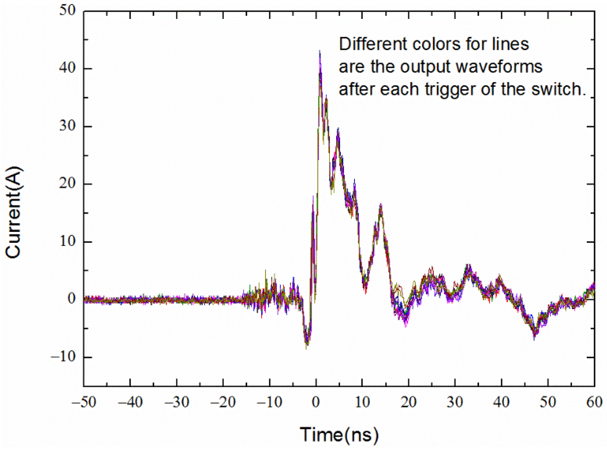
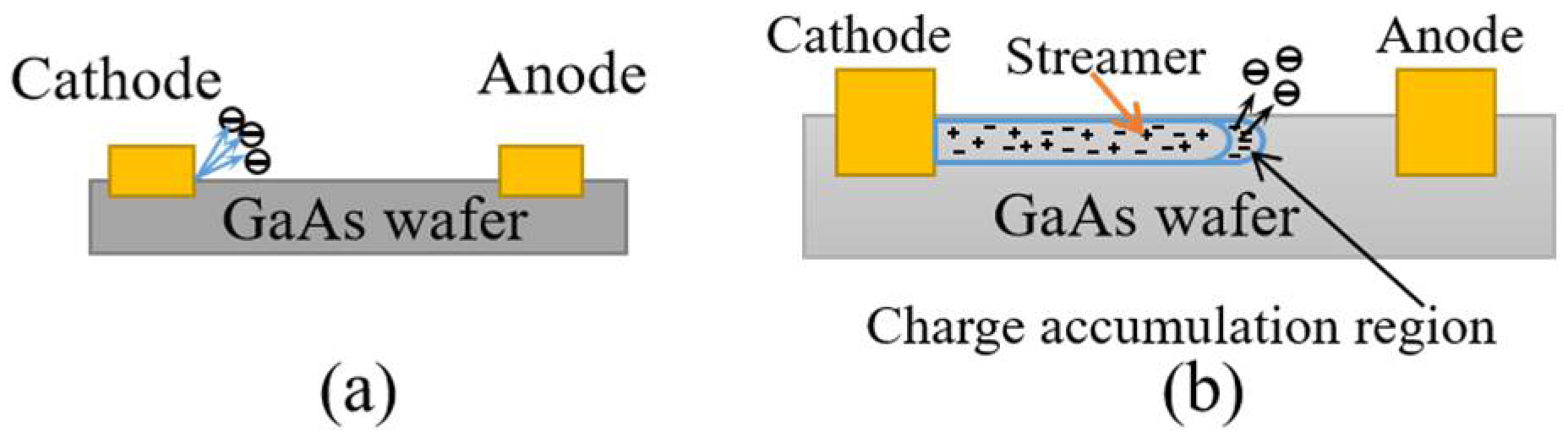
The structure diagram of the designed GaAs PCSS is shown in Figure 1. The switch chip is made of semi-insulating GaAs, which has a dark state resistivity of 5 × 10⁷ Ω·cm and electron mobility of 5000 cm2/(V·s). The chip has a thickness of 0.6 mm and a size of 16 mm × 10 mm. The electrode is made of Au/Ge/Ni, as it forms a good ohmic contact with the GaAs PCSS. Each electrode has a size of 6.0 mm × 3.0 mm, while the gap between the two electrodes is 10 mm. They feature two optimizations: the corners are rounded with a 1.1 mm radius (as shown in Figure 2a), and an optimal etch angle of 135° was used (as shown in Figure 2b). This structure allows reduction in the electric field intensity at the electrode edge, improving the withstand voltage strength of the GaAs PCSS.
In order to prevent flashover on the GaAs PCSS surface, we use a three-layer insulation package for the switch. The first layer, a 900 nm Si3N4 film is used to coat the GaAs PCSS surface to ensure sufficient insulation. The second layer, the GaAs PCSS chip, is packaged using transparent insulation glue, as shown in Figure 3. Finally, the GaAs PCSS was placed in insulating oils. After three layers of insulation package, the withstand voltage strength of the GaAs PCSS can be up to 40 kV.

3. Results

The device used to test the high-voltage GaAs PCSS is shown in Figure 4. The GaAs PCSS was triggered by a 1064 nm laser pulse generated by an Nd:YAG laser. The laser pulse width was 8 ns, and the laser was split into two equal energy portions by a 50/50 beam splitter. One beam was used to illuminate the GaAs PCSS gap between the GaAs PCSS electrodes, and another was measured using an optical energy meter.
The GaAs PCSS was placed in insulating oils, and a 30-pF capacitor was used. A current limiting resistor of 890 Ω was used in the capacitor discharge circuit to control the current. The discharge circuit current was measured using a current meter, Pearson Model 6027 (Pearson Electronics, CA, US ), and an oscilloscope with a 1-GHz bandwidth.
The 10-mm gap GaAs PCSS was charged by the capacitors and illuminated by a laser pulse at various bias voltages. The laser trigger parameters were as follows: the wavelength was 1064 nm, the beam energy was 137 μJ, and the spot size diameter was 4 mm. In addition, its position was fixed.
The output current waveforms at the bias voltage, ranging from 10 kV to 35 kV, are shown in Figure 5. In the experiment, linear and avalanche modes were distinguished based on the GaAs PCSS output waveform. The output current waveforms at the bias voltages of 10 kV, 15 kV, and 20 kV were similar to those of the laser pulse and had the same full pulse duration.
When the trigger energy was fixed, the output current was linearly related to the carrier drift velocity. The carrier drift velocity (vd) as a function of the bias field is shown in Figure 6 [25]. From Figure 6, the drift velocity reaches the saturation around 4 kV/cm. When the electric field is greater than 4 kV/cm, the carrier drift velocity decreases with the electric field. The carrier drift velocity reached 1.1 × 107 cm/s above 15 kV/cm. The degree of change in carrier drift velocity is becoming smaller and smaller, so the output current increases more and more slowly in linear mode.
The GaAs PCSS transitioned from the linear to avalanche mode when the bias voltage was higher than 25 kV. As shown in Figure 5, the peak current was 17.5 A, which was much higher than the linear current pulse at 20 kV. The rising edge was only 2.1 ns under the bias voltage of 25 kV, which was shorter than the laser pulse width. The results demonstrated that when the GaAs PCSS worked in the avalanche mode, the output current increased with the bias voltage. In the same operating mode, the electron-hole pairs excited by photons were ionized by the strong electric field, causing the avalanche multiplication effect.
The number of photo-excited carriers in the switch is hard to calculate accurately. To determine the avalanche ionization degree, it is necessary to define the avalanche multiplication rate (M), which can be used to describe the avalanche intensity.
The avalanche multiplication rate is expressed as:
M = N A / N L
where NA is the number of photo-excited carriers in the avalanche mode, and NL is the number of photo-excited carriers under high electrical field (>15 kV/cm) in the linear mode. The values of NA and NL can be, respectively calculated by:
N A = I A d t
N L = I L d t
According to Equation (1), the avalanche gains at the bias voltages of 30 kV and 35 kV are M30 = 1194 and M35 = 1385, respectively.
The equivalent circuit of the GaAs PCSS triggered by a laser is shown in Figure 7, where Rmin represents the minimum ON-state resistance of the GaAs PCSS, which can be calculated using the measured output peak current (Ipeak) and bias voltage (U) by the following expression:
R min = U I p e a k R
where R is the current-limiting resistor value and, in this work, its value is 890 Ω.
The semiconductor resistance converged quickly in the proposed configuration, as shown in Figure 8. When the GaAs PCSS operated in the high avalanche mode, the ON-state minimum resistance could reach the sub-Ohm level, achieving the value of 0.58 Ω under the bias voltage of 35 kV, which was lower than the value of 2.14 Ω reported in [26].
The 10-mm GaAs PCSS charged by a 30-pF capacitor was tested for stability at the bias voltages of 30 kV and 35 kV. The 10 repetitive output current waveforms are presented in Figure 9 and Figure 10. The results show that the proposed PCSS design has high stability. The jitter value can be used to quantitatively describe the avalanche stability [27,28,29,30]. The single PCSS jitter can be calculated by:
T = 1 n i = 1 n ( t i t ¯ ) 2
where ti denotes the delay time between the laser pulse and the output current waveform of trigger i, n is the number of triggers, and t is the average value of delay times of multiple triggers. The jitter values of the avalanche GaAs PCSS values calculated by Equation (5) were as follows: 164.3 ps at the bias voltage of 30 kV, and 106.9 ps at the bias voltage of 35 kV. Both results are shorter than the previously best-reported value of 560 ps [6].
Based on the experimental results, it can be concluded that the bias voltage has the dominant effect on the PCSS jitter. The higher the bias voltage is, the smaller the jitter will be. Reducing the jitter, in turn, improves the avalanche stability. In addition, the avalanche gain and ionization coefficient increase with the increase in the voltage, and the rising edge of the current waveform is shorter at higher avalanche gains.
In the air, the PCSS was prone to flashover along the surface at the bias voltage of above 30 kV. According to the secondary electron emission avalanche (SEEA) model [31], initial electrons are required for the formation of surface flashover. In the GaAs photoconductive switch, initial electrons required for surface flashover can be obtained in one of two ways. The first is according to the planar structure diagram of the GaAs PCSS; at the triple junction of the cathode, air, and chip surface, microscopic burrs can be found on both the electrode and chip’s surfaces. In the case of a high voltage, when the distortion and bias electric fields are superimposed and exceed the field intensity required to emit electrons, electrons are emitted from the three cathode junctions, insulating layer, and chip surface, as shown in Figure 11a. The second is ensuring the GaAs photoconductive switch works in a nonlinear mode. According to the filament current streamer model [32], in the early stage of streamer formation, photo-excited charge domains are formed due to the GaAs material’s rapid field characteristics. The charge domains can develop into the primary streamer, and a large number of electrons can be gathered in the streamer head, causing distortion in the electric field, which meets the requirements for the electric field electron emission. The streamer head emits electrons to the switch surface, providing initial electrons for flashover along the surface, as shown in Figure 11b.
To prevent switch surface flashover, the switch was encapsulated in three layers. The first layer was Si3N4 (on the switch surface), the second layer integrated the solid silicone gel, and the third layer included submerging the chip in insulation oil. The three-layer switch encapsulation significantly reduced the flashover phenomenon on the surface.

4. Conclusions

In this paper, a GaAs PCSS design is proposed to obtain high avalanche gain at high bias voltage (20 kV to 35 kV). The avalanche gain concept is proposed to determine the avalanche level using the experimentally obtained values and the ionization rate at different bias voltages. The obtained values of the maximum avalanche gain, maximum ionization rate, and minimum ON-state resistance of the GaAs PCSS are 1385 and 0.58 Ω, respectively. In addition, the influence of the bias voltage on the avalanche stability is analyzed. The stability calculation method is presented and used to calculate the jitter value of the proposed design. The results show that the jitter values at the bias voltages of 30 kV and 35 kV are 164.3 ps and 106.9 ps, respectively. This work can be used as a reference in the design of high-voltage pulse generators, and provides an idea for the future design of high-voltage GaAs PCSS photoconductance switches.

Author Contributions

Conceptualization, W.S. and C.M.; investigation, C.M.; M.W.; W.W. and Y.J.; writing—original draft preparation, C.M.; writing—review and editing, C.M. and M.W.; project administration, W.S.; funding acquisition, W.S. and C.M. All authors have read and agreed to the published version of the manuscript.

Funding

This work was supported in part by the National Natural Science Foundation of China under Grant No. 51807161, the State Key Laboratory of Intense Pulsed Radiation Simulation and Effect of China under Grant No. SKLIPR1812, the China Postdoctoral Science Foundation under Grant No. 2018M633547, and the Youth Innovation Team of Shaanxi Universities (21JP084).

Institutional Review Board Statement

Not applicable.

Informed Consent Statement

Not applicable.

Data Availability Statement

The data presented in this study are available on request from the corresponding author.

Conflicts of Interest

The authors declare no conflict of interest.

References

  1. Chang, C.; Liu, G.; Tang, C.; Chen, C.; Fang, J. Review of recent theories and experiments for improving high-powermicrowave window breakdown thresholds. Phys. Plasmas 2011, 18, 055702. [Google Scholar] [CrossRef]
  2. Ajram, S.; Salmer, G. Ultrahigh frequency DC-to-DC converters using GaAs Power switches. IEEE Trans. Power Electron. 2011, 16, 594. [Google Scholar] [CrossRef]
  3. Hudgins, J.L.; Simin, G.S.; Santi, E.; Khan, M.A. An assessment of wide bandgap semiconductors for power devices. IEEE Trans. Power Electron. 2003, 18, 2644. [Google Scholar] [CrossRef] [Green Version]
  4. Stygar, W.A.; Cuneo, M.E.; Headley, D.I.; Ives, H.C.; Leeper, R.J.; Mazarakis, M.G.; Olson, C.L.; Porter, J.L.; Wagoner, T.C.; Woodworth, J.R. Architecture of petawatt-class Z-pinch accelerators. Phys. Rev. Accel. Beams 2007, 10, 30401. [Google Scholar] [CrossRef] [Green Version]
  5. Schoenbach, K.H.; Xiao, S.; Joshi, R.P.; Camp, J.T.; Heeren, T.; Kolb, J.F.; Beebe, S.J. The effect of intense subnanosecond electrical pulses on biological cells. IEEE Trans. Plasma. Sci. 2008, 36, 414. [Google Scholar] [CrossRef]
  6. Glover, S.F.; Zutavern, F.J.; Swalby, M.E.; Cich, M.J.; Loubriel, G.M.; Mar, A.; White, F.E. Pulsed-and DC-charged PCSS-based trigger generators. IEEE Trans. Plasma Sci. 2010, 38, 2701. [Google Scholar] [CrossRef]
  7. Pala, V.; Peng, H.; Wright, P.; Hella, M.M.; Chow, T.P. Integrated high-frequency power converters based on GaAs pHEMT: Technology characterization and design examples. IEEE Trans. Power Electron. 2012, 27, 2644. [Google Scholar] [CrossRef]
  8. Islam, N.E.; Schamiloglu, E.; Fleddermann, C.B. Characterization of a semi-insulating GaAs photoconductive semiconductor switch for ultrawide band high power microwave applications. Appl. Phys. Lett. 1998, 73, 1988. [Google Scholar] [CrossRef]
  9. Lee, C.H. Picosecond optoelectronic switching in GaAs. Appl. Phys. Lett. 1977, 30, 84. [Google Scholar] [CrossRef]
  10. Zutavern, F.J.; Loubriel, G.M.; O’Malley, M.W.; Shanwald, L.P.; Helgeson, W.D.; McLaughlin, D.L.; McKenzie, B.B. Photo-conductive semiconductor switch experiments for pulsed power applications. IEEE Trans. Electron Dev. 1990, 37, 2742. [Google Scholar] [CrossRef]
  11. El Amari, S.; Kenaan, M.; Merla, C.; Vergne, B.; Arnaud-Cormos, D.; Leveque, P.; Couderc, V. Kilovolt, nanosecond, and picosecond electric pulse shaping by using optoelectronic switching. IEEE Photon. Technol. Lett. 2010, 22, 1577–1579. [Google Scholar] [CrossRef]
  12. Shi, W.; Tian, L.; Liu, Z.; Zhang, L.; Zhang, Z. 30 kV and 3 kA semi-insulating GaAs photoconductive semiconductor switch. Appl. Phys. Lett. 2008, 92, 043511. [Google Scholar] [CrossRef]
  13. Nunnally, W.C.; Hammond, R.B. 80 MW photoconductor power switch. Appl. Phys. Lett. 1984, 44, 980. [Google Scholar] [CrossRef]
  14. Tian, L.; Shi, W. Multiple charge domains model for the lock-on effect in GaAs power photoconductive switches. J. Phys. D Appl. Phys. 2008, 41, 115107. [Google Scholar] [CrossRef]
  15. Xu, M.; Li, R.; Ma, C.; Shi, W. 1.23-ns pulsewidth of quenched high gain GaAs photoconductive semiconductor switch at 8-nJ excitation. IEEE Electron Device Lett. 2016, 37, 1147–1149. [Google Scholar] [CrossRef]
  16. El Amari, S.; De Angelis, A.; Arnaud-Cormos, D.; Couderc, V.; Leveque, P. Characterization of a linear photoconductive switch used in nanosecond pulsed electric field generator. IEEE Photon. Technol. Lett. 2011, 23, 673. [Google Scholar] [CrossRef]
  17. Zhao, F.; Islam, M.M.; Muzykov, P.; Bolotnikov, A.; Sudarshan, T.S. Optically activated 4H-SiC p-i-n diodes for high-power applications. IEEE Electron Device Lett. 2009, 30, 1182. [Google Scholar] [CrossRef]
  18. Kelkar, K.S.; Islam, N.E.; Fessler, C.M.; Nunnally, W.C. Silicon carbide photoconductive switch for high-power linear-mode opera-tions through sub-band-gap triggering. J. Appl. Phys. 2005, 98, 093102. [Google Scholar] [CrossRef]
  19. Dogan, S.; Teke, A.; Huang, D.; Morkoc, H. 4H-SiC photoconductive switching devices for use in high-power applications. Appl. Phys. Lett. 2003, 82, 3107. [Google Scholar] [CrossRef]
  20. Sullivan, J.S.; Stanley, J.R. 6H-SiC photoconductive switches triggered at below bandgap wavelengths. IEEE Trans. Dielectr. Electr. Insul. 2007, 14, 980. [Google Scholar] [CrossRef] [Green Version]
  21. Jiang, S.; Song, C.; Zhang, L.; Zhang, Y.; Huang, W.; Guo, H. Intrinsic photoconductive switches based on semi-insulator 4H-SiC. IEEE Trans. Electron Devices 2016, 63, 1582. [Google Scholar] [CrossRef]
  22. Han, W.-W.; Huang, W.; Zhuo, S.-Y.; Xin, J.; Liu, X.-C.; Shi, E.-W.; Zhang, Y.-F.; Cao, P.-H.; Wang, Y.-T.; Guo, H.; et al. A new method of accurately measuring photoconductive performance of 4H-SiC photoconductive switches. IEEE Electron. Device Lett. 2018, 40, 271. [Google Scholar] [CrossRef]
  23. Ma, C.; Shi, W.; Li, M.; Gui, H.; Wang, L.; Jiang, H.; Fu, Z.; Cao, J. Research on flashover characteristics and the physical mechanism of high-gain GaAs photoconductive switches. IEEE J. Quantum Electron. 2014, 50, 568–574. [Google Scholar] [CrossRef]
  24. Wang, S.; Shi, W. The role of the photo-generated carrier in surface flashover of the GaAs photoconductive semiconductor switch. IEEE J. Electron. Devices Soc. 2017, 6, 179. [Google Scholar] [CrossRef]
  25. Rosen, A. High-Power Optically Activated Solid-State Switches; Zutavern, F., Ed.; Artech House: Boston, MA, USA, 1994; p. 44. [Google Scholar]
  26. Xiao, L.; Hu, X.; Chen, X.; Peng, Y.; Yang, X.; Xu, X. Effect of periodic array on the on-state resistances of GaAs photoconductive semiconductor switch based on total reflection theory. AIP Adv. 2017, 7, 065119. [Google Scholar] [CrossRef] [Green Version]
  27. Shi, W.; Gui, H.; Zhang, L.; Ma, C.; Li, M.; Xu, M.; Wang, L. Effects of trigger laser pulse width on the jitter time of GaAs photoconductive semiconductor switch. Opt. Lett. 2013, 38, 2330–2332. [Google Scholar] [CrossRef]
  28. Shi, W.; Gui, H.-M.; Zhang, L.; Li, M.-X.; Ma, C.; Wang, L.-Y.; Jiang, H. Influence of the incident laser pulse energy on jitter time of GaAs photoconductive semiconductor switches. Opt. Lett. 2013, 38, 4339–4341. [Google Scholar] [CrossRef]
  29. Gaudet, J.A.; Skipper, M.C.; Abdalla, M.D.; Ahern, S.M.; Romero, S.P.; Mar, A.; Zutavern, F.J.; Loubriel, G.M.; O’Malley, M.W.; Helgeson, W.D. Temporal switching jitter in photoconductive switches. Proc. SPIE 2000, 4301, 121. [Google Scholar]
  30. Shi, W.; Zhang, L.; Gui, H.; Hou, L.; Xu, M.; Qu, G. Accurate measurement of the jitter time of GaAs photoconductive semiconductor switches triggered by a one-to-two optical fiber. Appl. Phys. Lett. 2013, 102, 154106. [Google Scholar] [CrossRef]
  31. Anderson, R.A.; Branard, J.P. Mechanism of pulsed surface flashover involving electron-stimulated desorption. J. Appl. Phys. 1980, 51, 1414. [Google Scholar] [CrossRef]
  32. Shi, W.; Ma, C.; Hou, L.; Xie, G.; Tian, L.; Wu, S. Velocity of current filament at the high gain mode of GaAs power photoconductive switches. Physica B 2011, 406, 3741. [Google Scholar] [CrossRef]
Figure 1. High-avalanche SI-GaAs PCSS structure.
Photonics 08 00385 g001
Figure 2. Schematic diagram of the SI-GaAs PCSS electrodes: (a) Top view of electrodes; (b) Side profile of electrodes.
Photonics 08 00385 g002
Figure 3. Cross-section of the SI-GaAs PCSS.
Photonics 08 00385 g003
Figure 4. GaAs PCSS testing circuit.
Photonics 08 00385 g004
Figure 5. Output current waveforms under various bias voltages.
Photonics 08 00385 g005
Figure 6. Carrier drift velocity as a function of the bias field.
Photonics 08 00385 g006
Figure 7. Equivalent circuit of the GaAs PCSS triggered by a laser.
Photonics 08 00385 g007
Figure 8. GaAs PCSS resistance versus the bias voltage.
Photonics 08 00385 g008
Figure 9. Ten repetitive output waveforms of the 10 mm GaAs PCSS biased at 30 kV.
Photonics 08 00385 g009
Figure 10. Ten repetitive output waveforms of the 10 mm GaAs PCSS biased at 35 kV.
Photonics 08 00385 g010
Figure 11. (a) Schematic diagram of the field electron emission around the cathode triple junction. (b) Schematic diagram of the field electron emission of the streamer head.
Photonics 08 00385 g011
Publisher’s Note: MDPI stays neutral with regard to jurisdictional claims in published maps and institutional affiliations.

