Miniaturized Interferometric Sensors with Spectral Tunability for Optical Fiber Technology—A Comparison of Size Requirements, Performance, and New Concepts

 ,
,  , , ,
, , , 
Abstract
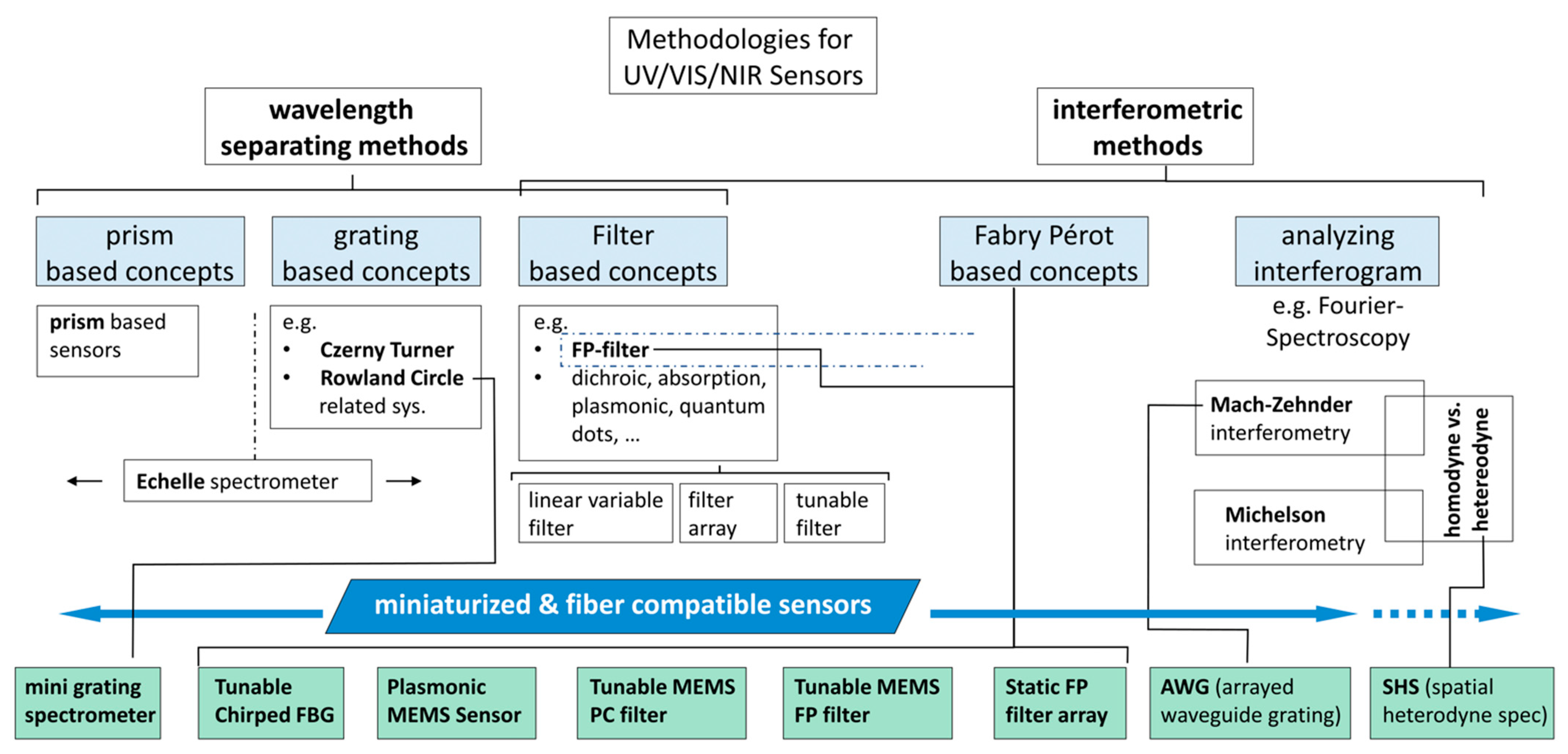
:1. Introduction
2. Methodology of Static FP Sensor Arrays
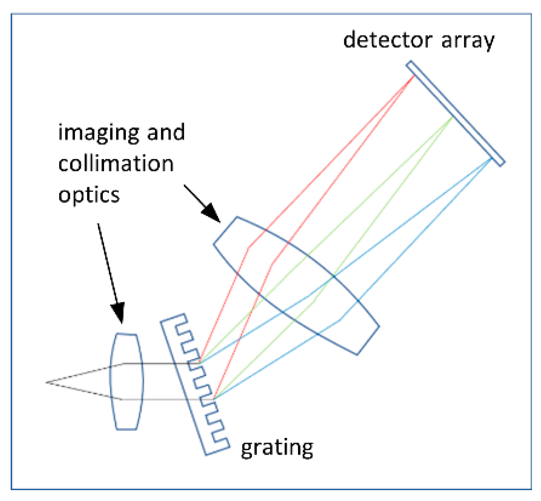
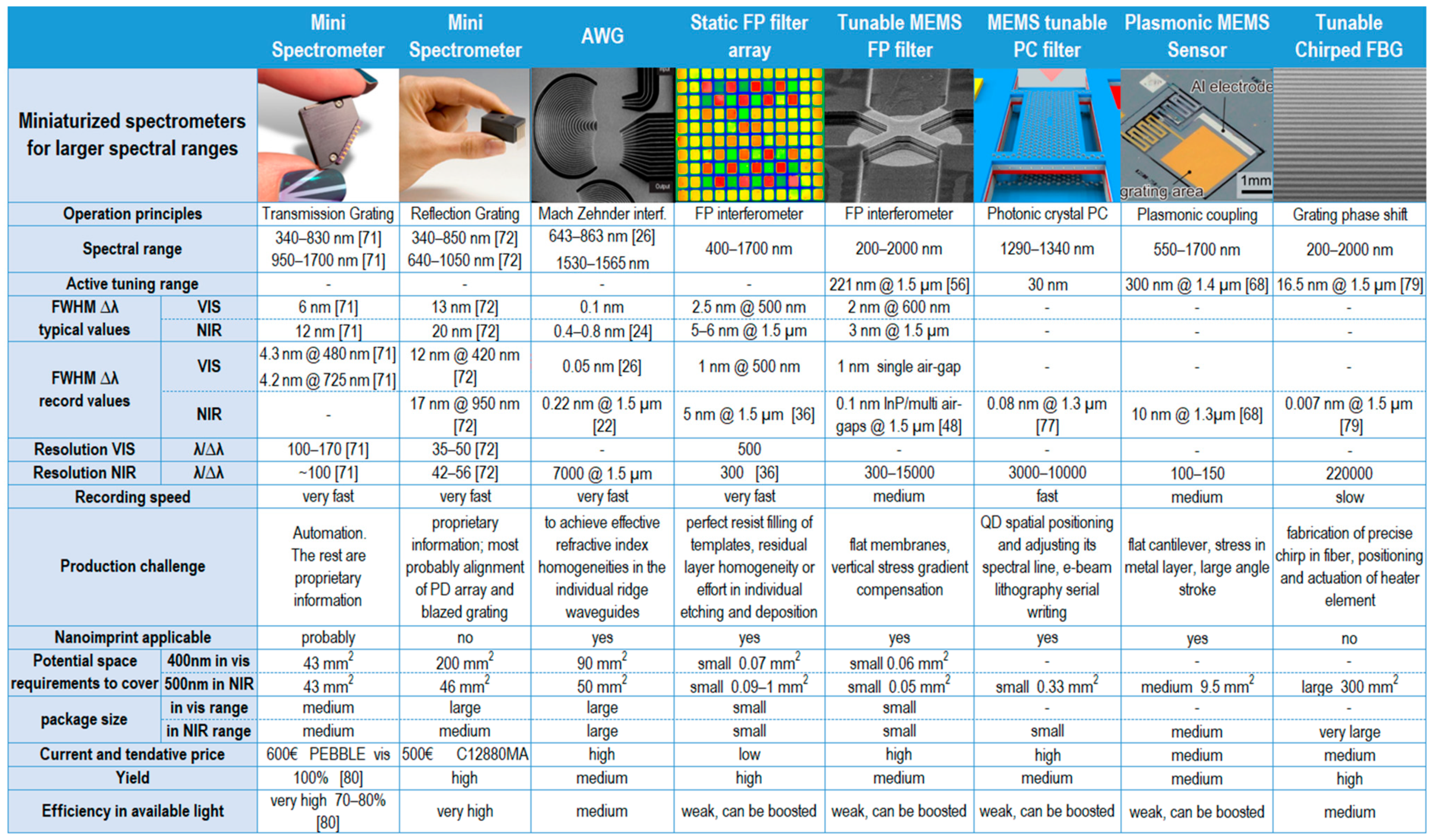
2.1. Microspectrometers
2.2. Nanospectrometers
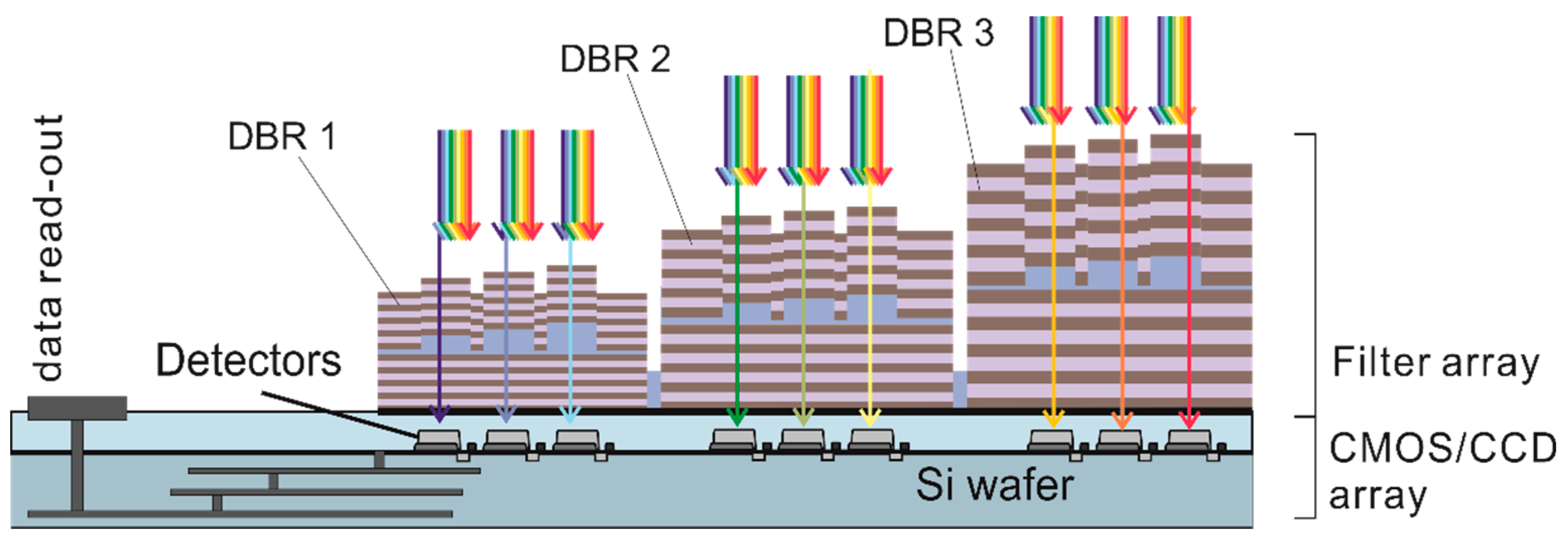
3. Static FP Filter Array Fabrication in the VIS Spectral Range Demonstrating a Single Nanoimprint over 3 DBR Stacks of Different Height
3.1. DBR Mirrors: Materials and Geometrical Issues
3.2. Definition of 3D Nanoimprint Templates Using Digital Etching and Digital Deposition
3.3. Combining Three DBR Stopbands in the Fabrication Process of an FP Filter Array
3.4. The Complete Array: Lateral Arrangement of the FP Filters
4. Experimental Results of Static FP Filter Arrays in the VIS Range
4.1. Transmission Spectra of Static FP Filter Arrays
4.2. Interpretation of Experimental Results Concerning Linewidths
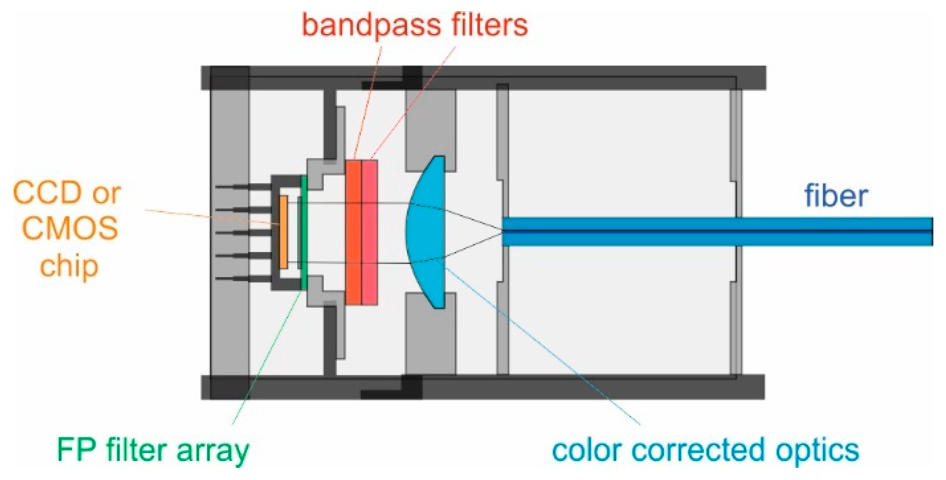
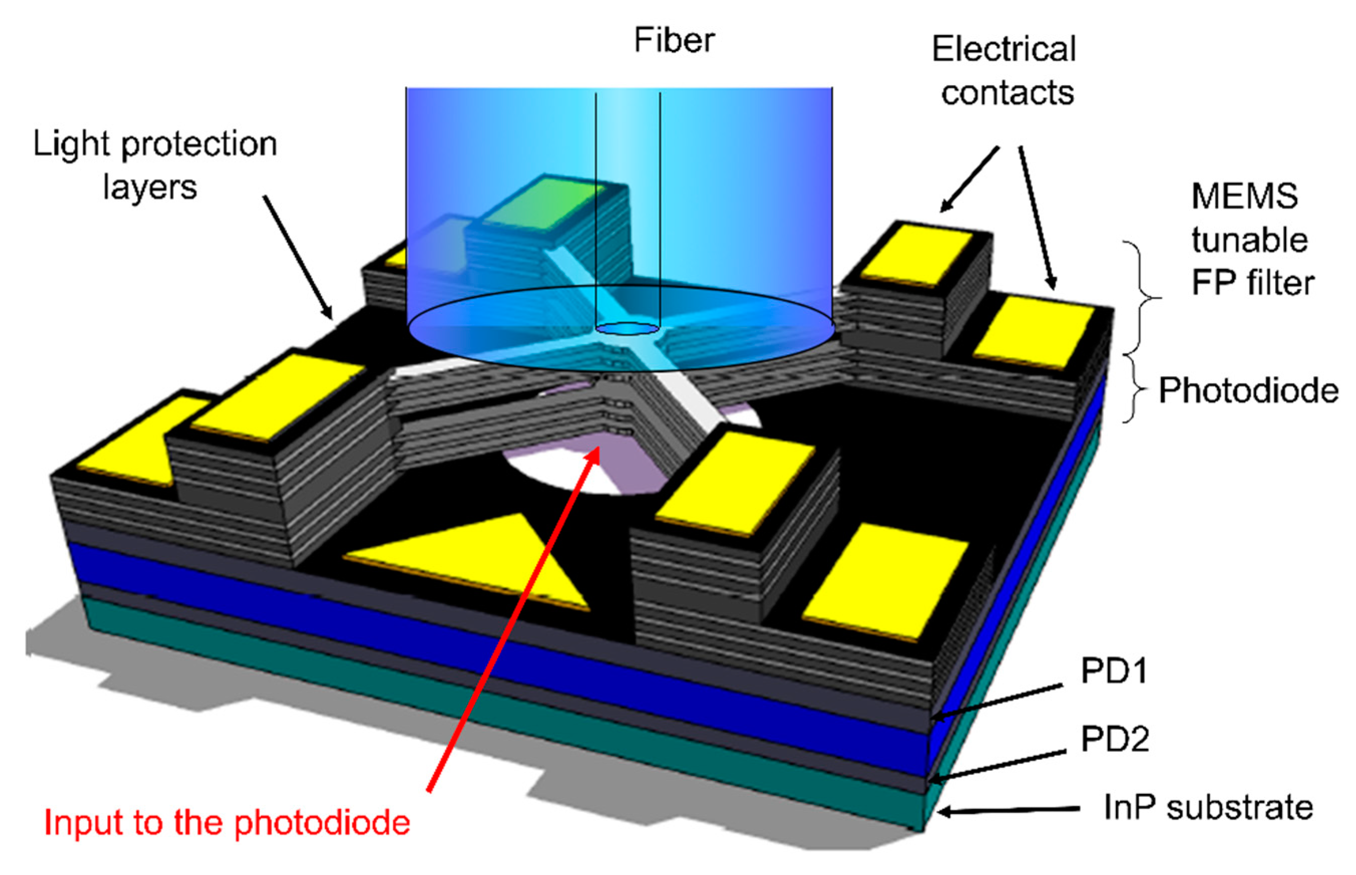
5. Static FP Sensor Array in a Fiber Technology System
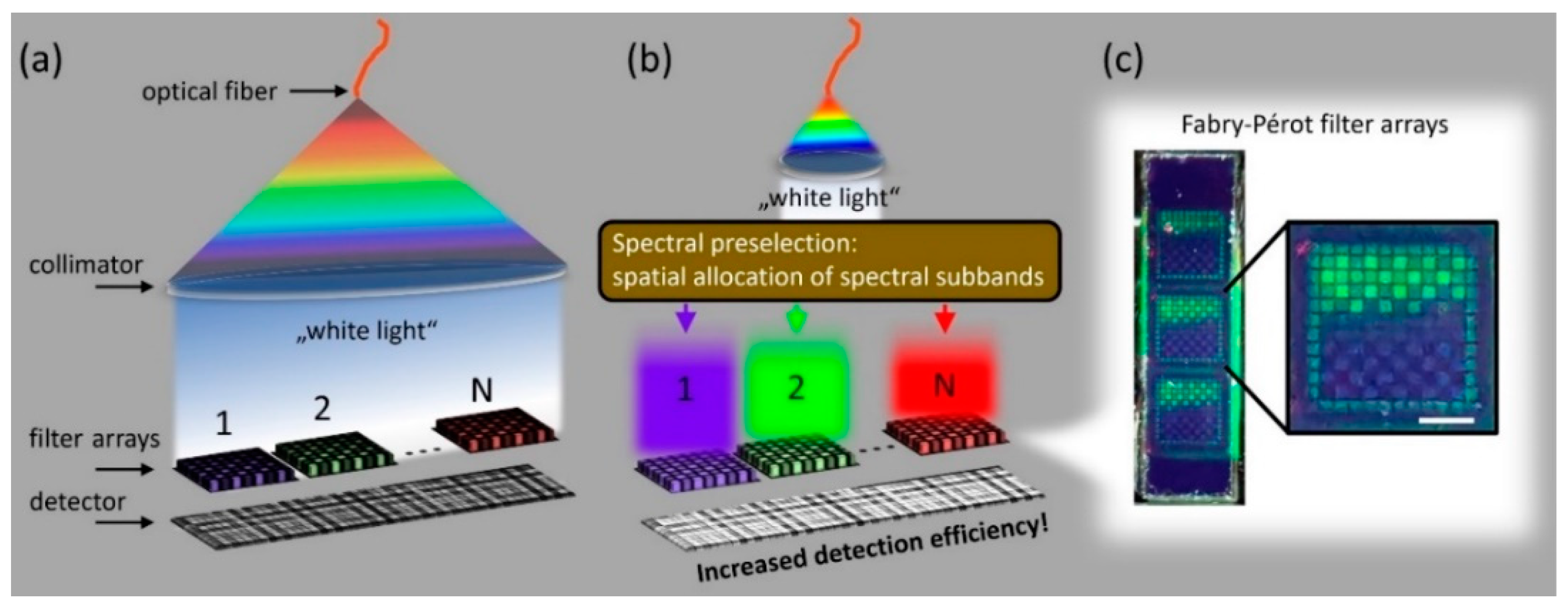
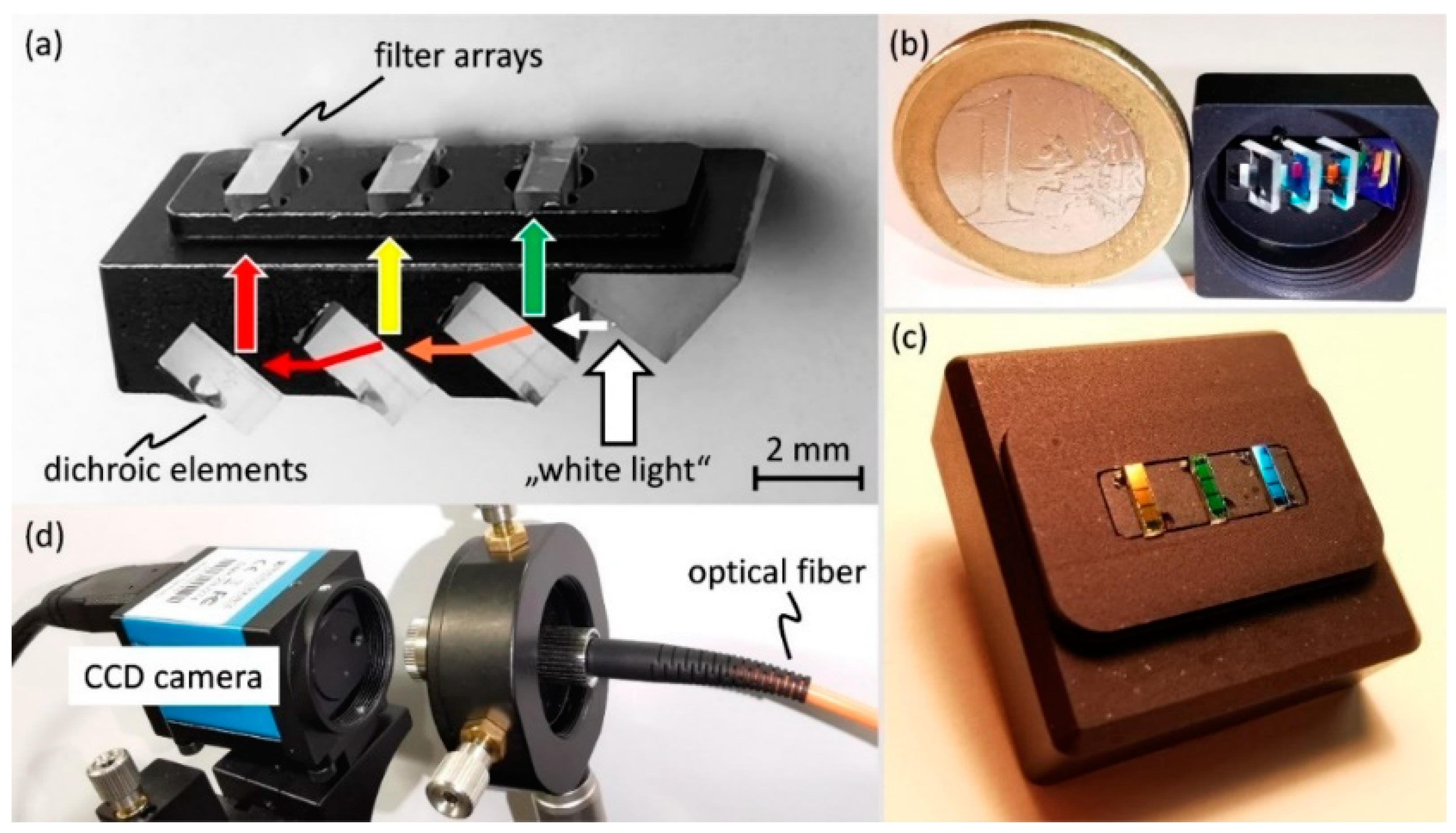
6. Laboratory Demonstration of Efficiency Boosting by Spectral Preselection
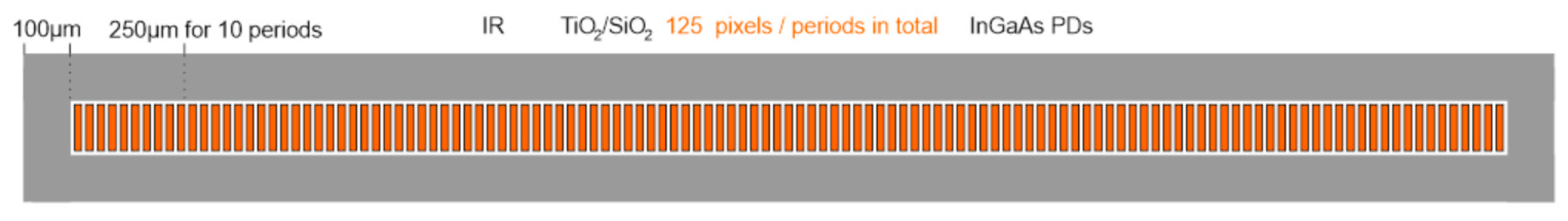
7. Static FP Filter Arrays for the NIR: Fabrication and Characterization
8. MEMS Tunable FP Filters with a Single Air-Gap for the VIS and NIR Spectral Range
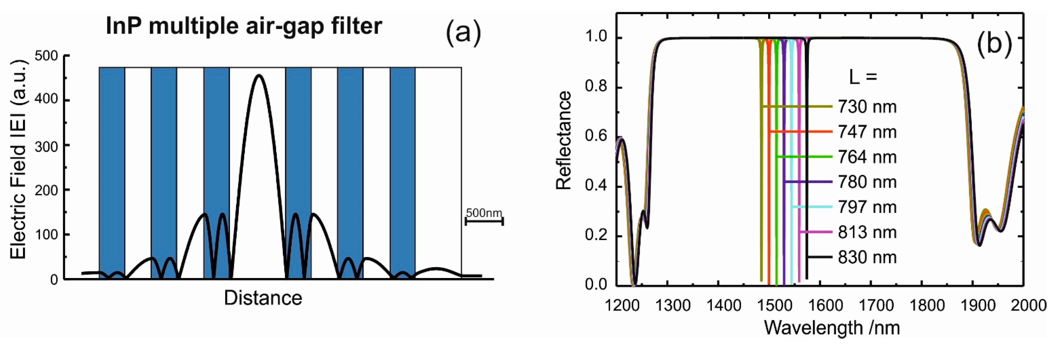
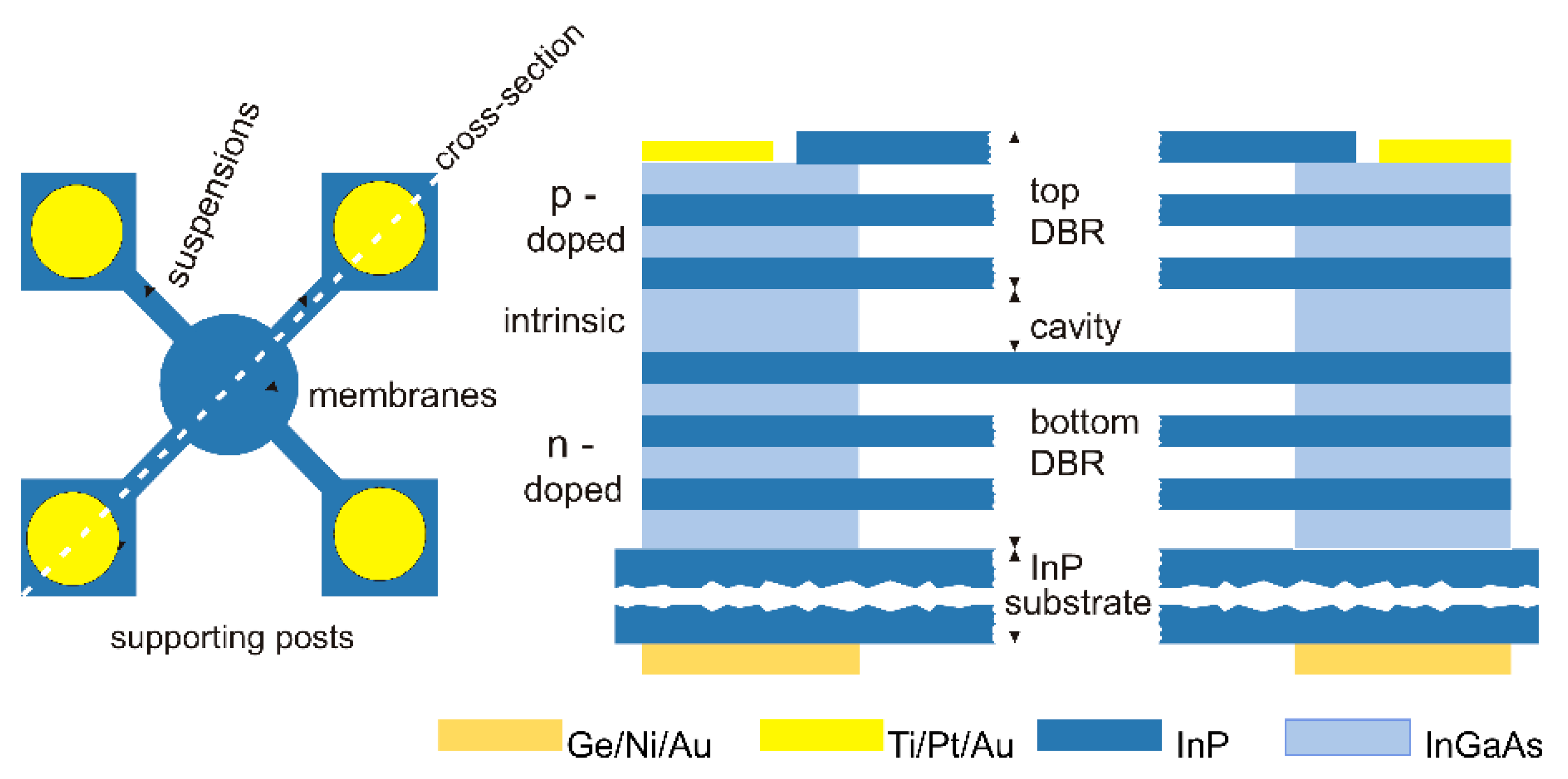
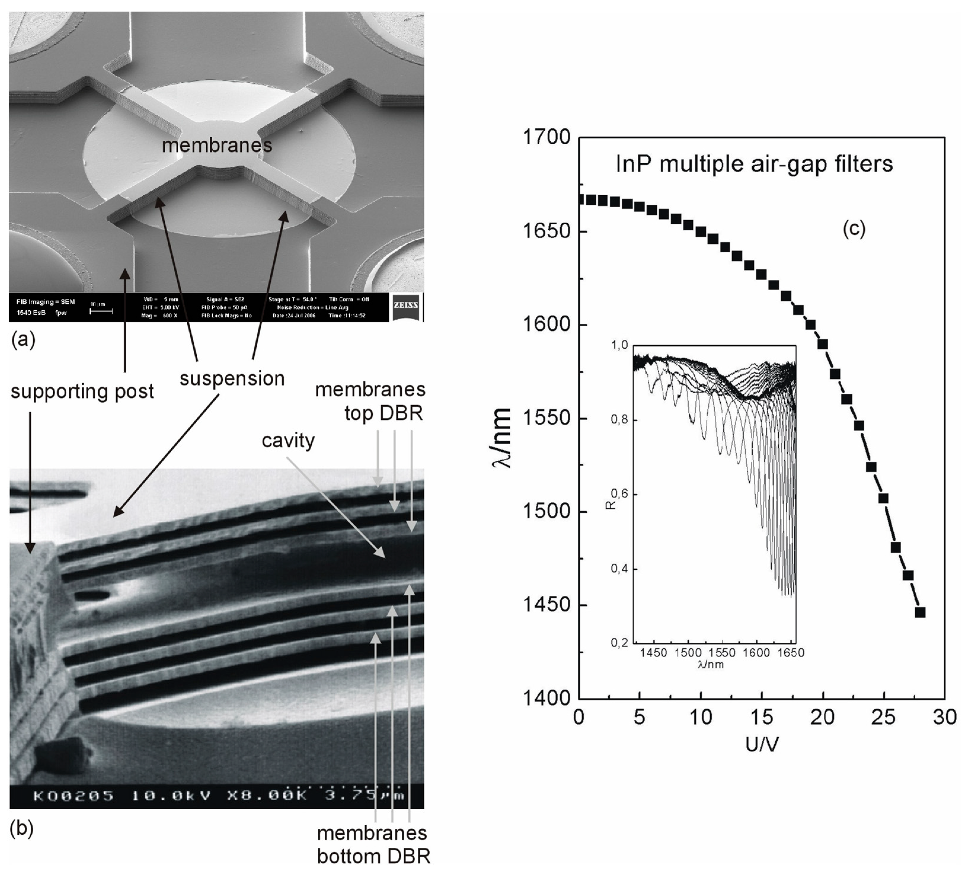
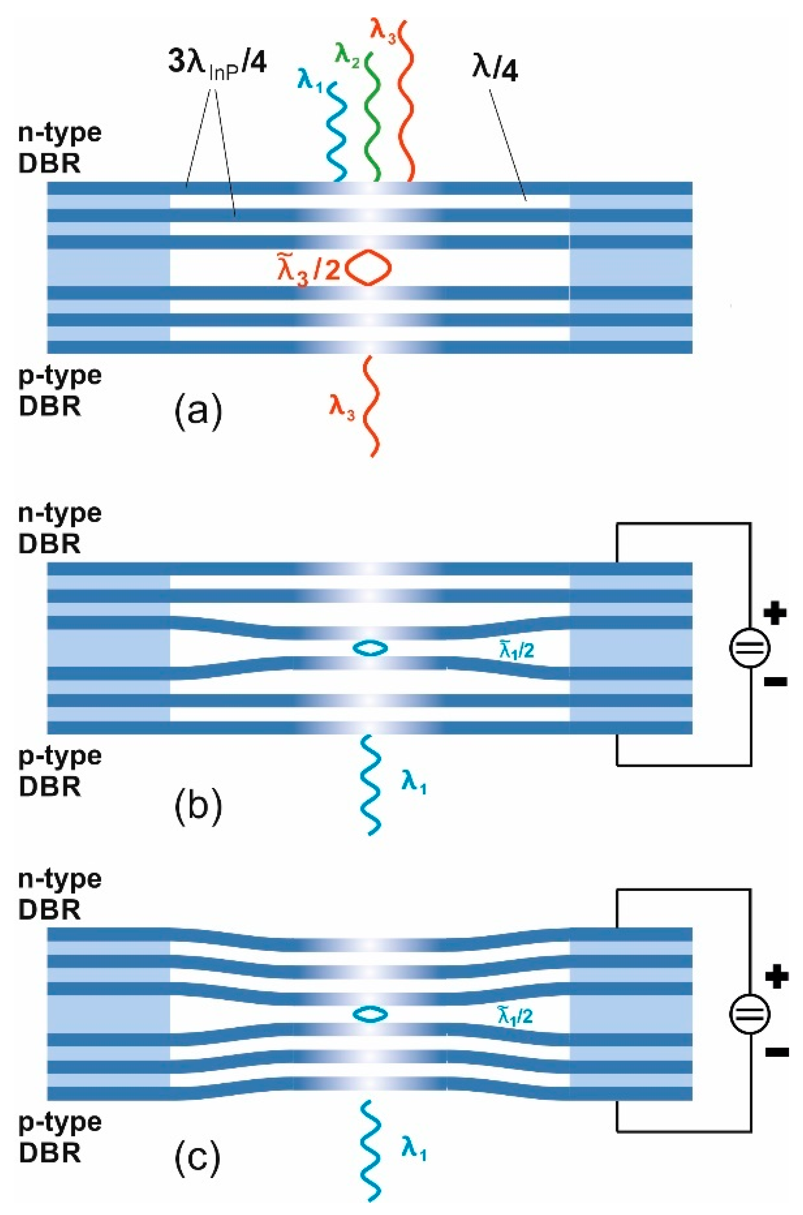
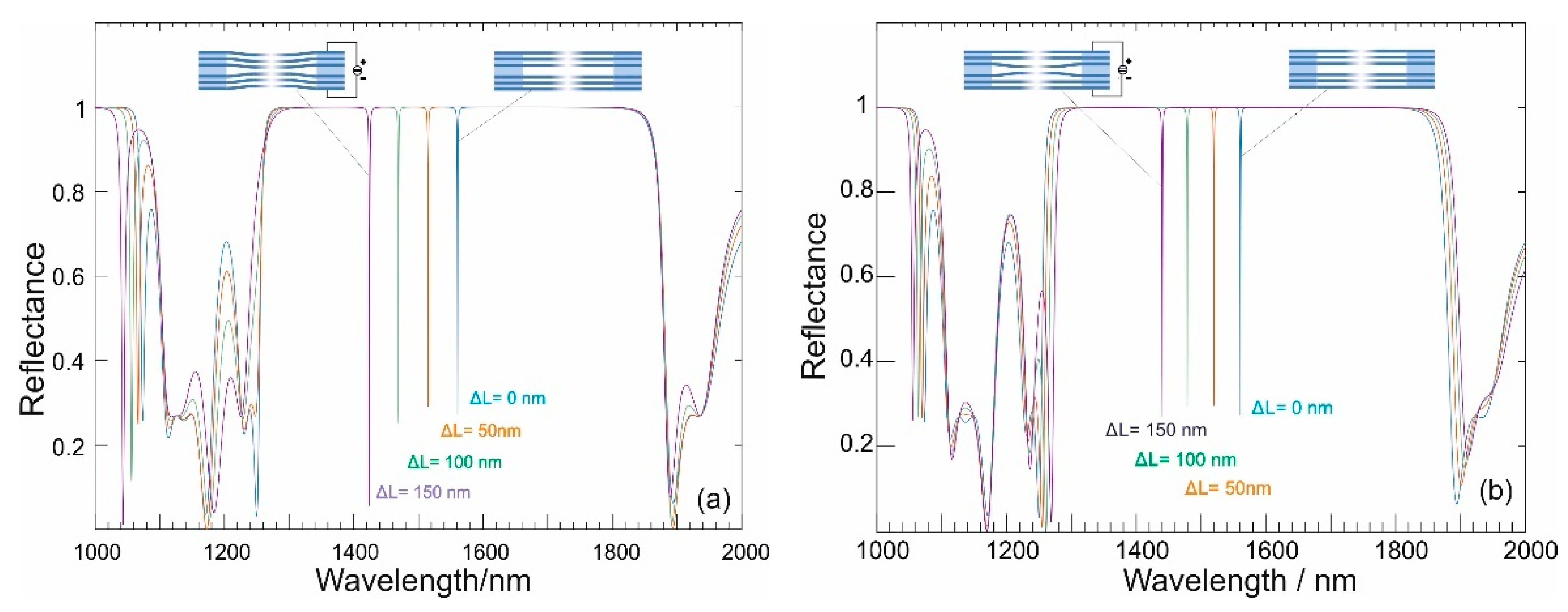
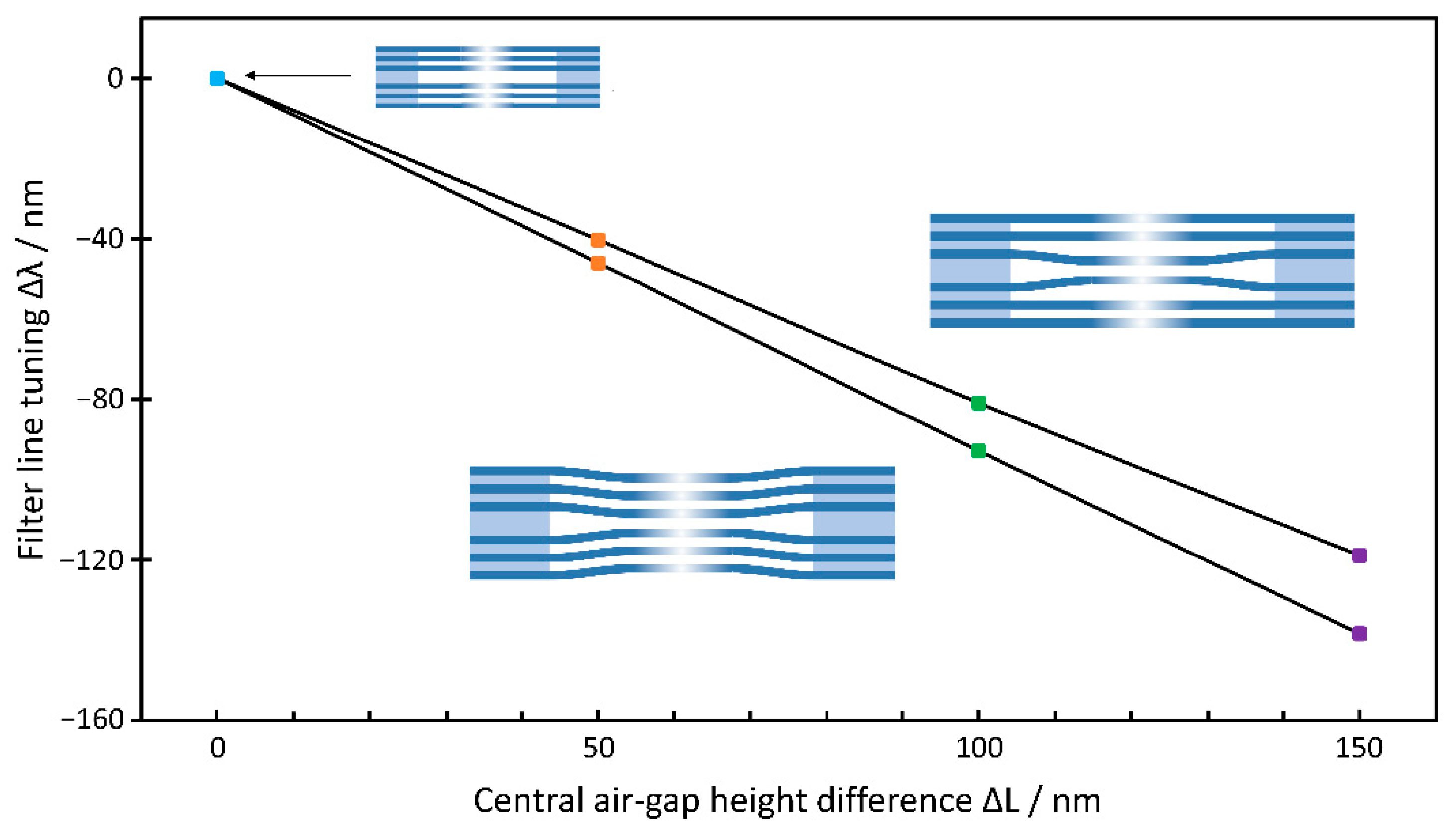
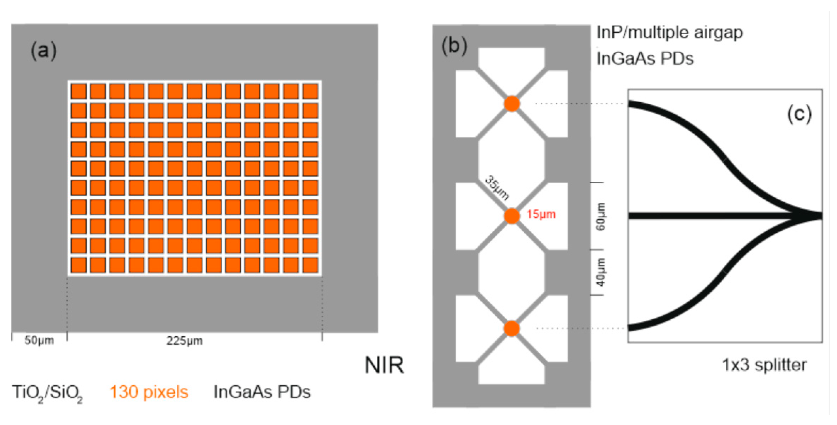
9. MEMS Tunable FP Filter Sensors in the NIR Range with Multiple Air-Gaps: Methodology, Simulations, Fabrication and Characterization
10. Limits of Semiconductor and Dielectric Material Systems for MEMS-Based Sensorics: Geometry, FWHM, Tuning and Stopband Width
11. Further Concepts for Miniaturization Based on Plasmonics, Ring Resonators, Quantum Dots, Spatial Heterodyning, and Photonic Crystals on Fiber Tips and in MEMS Membranes
11.1. Sensors Based on Photonic Crystals in MEMS Membranes
11.2. Nano-Optical Sensor Concepts
11.3. Sensors with Links to Telecom Devices
11.4. Sensors with Computational Signal Evaluation
11.5. Sensors on the Fiber Tip
11.6. Spatial Heterodyne Sensors
12. Estimation of Potential Space Requirement after Utmost Miniaturization
12.1. Static FP Filter Arrays Covering 400 nm in the VIS Spectral Range
12.2. Static FP Filter Arrays Covering 500 nm in the NIR Spectral Range
12.3. MEMS Tunable FP Filter Arrays Covering 500 nm in the NIR Spectral Range
12.4. MEMS Tunable FP Filter Arrays Covering 400 nm in the VIS Spectral Range
12.5. MEMS Tunable PC Filter to Cover a Spectral Span of 500 nm in the NIR Range
12.6. AWG Covering 500 nm in the NIR Spectral Range
12.7. Plasmonic MEMS Cantilever Covering 500 nm in the NIR Spectral Range
12.8. Locally Heated Chirped FBG to Cover a Spectral Span of 500 nm in the NIR Spectral Range
13. Where Are the Minimum Structure Size Limits in 3D Nanoimprint Lithography?
14. Can Nanoimprint Be Applied to Fabricate the Seven Sensor Types Compared Here?
15. Conclusions
16. Patents
Author Contributions
Funding
Institutional Review Board Statement
Informed Consent Statement
Data Availability Statement
Acknowledgments
Conflicts of Interest
Abbreviations
| 1D | one-dimensional |
| 2D | two-dimensional |
| 3D | three-dimensional |
| αInP | absorption coefficient of InP |
| αSi3N4 | absorption coefficient of silicon nitride |
| αSiO2 | absorption coefficient of silicon dioxide |
| AWG | arrayed waveguide grating |
| CCD | charge coupled device |
| CMOS | complementary metal oxide semiconductor |
| Δλ | wavelength tuning range, wavelength interval, wavelength difference |
| Δλi | wavelength interval, wavelength spacing |
| Δλ/λ | optical resolution of an optical sensor or spectrometer |
| Δl | interface fluctuations |
| ΔL | displacement of DBR mirrors, cavity tuning |
| ΔL1, ΔL2 | cavity lengths fluctuations |
| Δλ/ΔL | tuning efficiency |
| Δn | refractive index difference |
| DBR | distributed Bragg reflector |
| DWDM | dense wavelength division multiplex |
| FBG | fiber Bragg grating |
| FIB | focused ion beam |
| FP | Fabry-Pérot |
| FWHM | full width at half maximum, linewidth |
| GMR | guided mode resonance |
| L, L1, L2 | cavity thickness, cavity height, cavity length |
| λ | vacuum wavelength |
| λair | wavelength of light in air |
| λi | central wavelength of DBR number i |
| λi/4 | quarter-wavelength optical thickness of a single DBR material layer of index i |
| effective wavelength | |
| λInP | wavelength of light in InP |
| Λ | periodicity of interference pattern |
| LIGA | Lithographie, Galvanik, Abformung = lithography, electroplating, molding |
| LPP | localized plasmon polariton |
| M | number of waveguides in an AWG |
| MEMS | micro-electro-mechanical-system |
| MOCVD | metal-organic chemical vapor deposition |
| n | refractive index |
| nInP | refractive index of indium phosphide |
| nSi3N4 | refractive index of silicon nitride |
| nSiO2 | refractive index of silicon dioxide |
| N | number of grating lines, or number of different FP filter arrays |
| NIR | near-infrared |
| QD | quantum dot |
| p | number of periods in the DBR |
| PC | photonic crystal |
| PCF | photonic crystal fiber |
| PD | photodiode |
| PD1, PD2 | highly doped semiconductor layers in a photodiode |
| PDMS | polydimethylsiloxane |
| PECVD | plasma enhanced chemical vapor deposition |
| Rmax | Maximum reflectance in the center of the stopband |
| Rmax,sat | Saturation value of the maximum reflectance in the center of the stopband |
| SCIL | substrate conformal imprint lithography |
| SEM | scanning electron microscope |
| SERS | surface enhanced Raman spectroscopy |
| SHS | spatial heterodyne spectroscopy |
| SOI | silicon on insulator |
| SPP | surface plasmon polariton |
| Θ | half angle between intersecting wavevectors |
| VIS | visible (spectral range) |
| UV | ultraviolet |
References
- Lindon, J.C.; Tranter, G.E.; Koppenaal, D. Encyclopedia of Spectroscopy and Spectrometry, 3rd ed.; Academic Press: Cambridge, MA, USA, 2016; ISBN 978-0-12-803224-4. [Google Scholar]
- Haken, H.; Wolf, H.C. Modern Methods of Optical Spectroscopy. In The Physics of Atoms and Quanta; Springer: Berlin, Heidelberg, Germany, 1996. [Google Scholar] [CrossRef]
- Baeten, V.; Dardenne, P. Spectroscopy: Developments in Instrumentation and Analysis. Grasas Aceites 2002, 53, 45–63. [Google Scholar] [CrossRef]
- Tkachenko, N.V. Optical Spectroscopy: Methods and Instrumentations, 1st ed.; Elsevier: Amsterdam, The Netherlands, 2006; ISBN 978-0-444-52126-2. [Google Scholar]
- Dakin, J.P.; Chambers, P. Review of Methods of Optical GAS detection by Direct Optical Spectroscopy, with Emphasis on Correlation Spectroscopy. In Optical Chemical Sensors; NATO Science Series; II: Mathematics, Physics and Chemistry; Baldini, F., Chester, A., Homola, J., Martellucci, S., Eds.; Springer: Dordrecht, The Netherlands, 2006; Volume 224, pp. 457–477. ISBN 978-1-4020-4609-4. [Google Scholar]
- Hodgkinson, J.; Tatam, R.P. Optical gas sensing: A review. Meas. Sci. Technol. 2013, 24, 012004. [Google Scholar] [CrossRef] [Green Version]
- Rolinger, L.; Rüdt, M.; Hubbuch, J. A critical review of recent trends, and a future perspective of optical spectroscopy as PAT in biopharmaceutical downstream processing. Anal. Bioanal. Chem. 2020, 412, 2047–2064. [Google Scholar] [CrossRef] [Green Version]
- Neumann, W. Fundamentals of Dispersive Optical Spectroscopy Systems; Society of Photo-Optical Instrumentation Engineers (SPIE): Bellingham, WA, USA, 2013; PM242; ISBN 978-081-949-824-3. [Google Scholar]
- Appenzeller, I. Optical-Range Grating and Prism Spectrometers. In Introduction to Astronomical Spectroscopy (Cambridge Observing Handbooks for Research Astronomers); Cambridge University Press: Cambridge, UK, 2012; pp. 81–126. [Google Scholar] [CrossRef]
- Thorne, A.P. Dispersion and resolving power: Prism spectrographs. In Spectrophysics; Springer: Dordrecht, The Netherlands, 1988. [Google Scholar] [CrossRef]
- Hillmer, H.; Woidt, C.; Istock, A.; Kobylinskiy, A.; Nguyen, D.T.; Ahmed, N.; Brunner, R.; Kusserow, T. Role of Nanoimprint Lithography for Strongly Miniaturized Optical Spectrometers. Nanomaterials 2021, 11, 164. [Google Scholar] [CrossRef]
- Kenda, A.; Frank, A.; Kraft, M.; Tortschanoff, A.; Sandner, T.; Schenk, H.; Scherf, W. Compact High-Speed Spectrometers Based on MEMS Devices with Large Amplitude In-Plane Actuators. Procedia Chem. 2009, 1, 556–559. [Google Scholar] [CrossRef]
- Tormen, M.; Lockhart, R.; Niedermann, P.; Overstolz, T.; Hoogerwerf, A.; Mayor, J.-M.; Pierer, J.; Bosshard, C.; Ischer, R.; Voirin, G.; et al. MEMS tunable grating micro-spectrometer. In Proceedings of the International Conference on Space Optics—ICSO, Toulouse, France, 14–17 October 2008; Society of Photo-Optical Instrumentation Engineers (SPIE): Bellingham, WA, USA, 2008; p. 1056607. [Google Scholar] [CrossRef] [Green Version]
- Huang, J.; Wen, Q.; Nie, Q.; Chang, F.; Zhou, Y.; Wen, Z. Miniaturized NIR Spectrometer Based on Novel MOEMS Scanning Tilted Grating. Micromachines 2018, 9, 478. [Google Scholar] [CrossRef] [Green Version]
- Truxal, S.T.; Kurabayashi, K.; Tung, J.-C. Design of a MEMS Tunable Polymer Grating for Single Detector Spectroscopy. Int. J. Optomechatronics 2008, 2, 75–87. [Google Scholar] [CrossRef]
- Harmon, K. Interferometers: Fundamentals, Methods and Applications (Physics Research and Technology); Nova Science Publishers: Hauppauge, NY, USA, 2015; ISBN 978-1-63483-692-0. [Google Scholar]
- Hariharan, P. Basics of Interferometry; Academic Press: Boston, MA, USA, 1992; ISBN 978-012-325-218-0. [Google Scholar]
- Andersson, P.O.; Edwall, G.; Persson, A.; Thylén, L. Fiber Optic Mach-Zehnder Interferometer Based on Lithium Niobate Components. In Integrated Optics; Springer Series in Optical, Sciences; Nolting, H.P.J., Ulrich, R., Eds.; Springer: Berlin/Heidelberg, Germany, 1985; Volume 48, pp. 26–28. ISBN 978-3-540-39452-5. [Google Scholar]
- Zetie., K.P.; Adams, S.F.; Tocknell, R.M. How does a Mach-Zehnder interferometer work? Phys. Educ. 2000, 35, 46–48. [Google Scholar] [CrossRef] [Green Version]
- Russel, J.; Cohn, R. Mach-Zehnder Interferometer; Book on Demand: Norderstedt, Germany, 2013; ISBN 978-551-267-842-8. [Google Scholar]
- Smit, M.K.; van Dam, C. PHASAR-Based WDM-Devices: Principles, Design and Applications. IEEE J. Sel. Top. Quantum Electron. 1996, 2, 236–250. [Google Scholar] [CrossRef] [Green Version]
- Kohtoku, M.; Sanjoh, H.; Oku, S.; Kadota, Y.; Yoshikuni, Y.; Shibata, Y. InP-based 64-channel arrayed waveguide grating with 50GHz channel spacing and up to −20dB crosstalk. Electron. Lett. 1997, 33, 1786–1787. [Google Scholar] [CrossRef]
- Kohtoku, M.; Sanjoh, H.; Oku, S.; Kadota, Y.; Yoshikuni, Y. Polarization Independent Semiconductor Arrayed Waveguide Gratings Using a Deep-Ridge Waveguide Structure. IEICE Trans. Electron. 1998, E81-C, 1195–1204. [Google Scholar]
- Yoshikuni, Y. Semiconductor Arrayed Waveguide Gratings for Photonic Integrated Devices. IEEE J. Sel. Top. Quantum Electron. 2002, 8, 1102–1114. [Google Scholar] [CrossRef]
- Cvetojevic, N.; Jovanovic, N.; Bland-Hawthorn, J.; Haynes, R.; Lawrence, J. Miniature Spectrographs: Characterization of Arrayed Waveguide Gratings for Astronomy. Proc. SPIE Int. Soc. Opt. Eng. 2010, 77394H. [Google Scholar] [CrossRef] [Green Version]
- Seyringer, D.; Sagmeister, M.; Maese-Novo, A.; Eggeling, M.; Rank, R.; Muellner, P.; Hainberger, R.; Drexler, W.; Vlaskovic, M.; Zimmermann, H.; et al. Technological verification of size-optimized 160-channel silicon nitride-based AWG-spectrometer for medical applications. Appl. Phys. B 2019, 125, 88. [Google Scholar] [CrossRef] [Green Version]
- Muneeb, M.; Ruocco, A.; Malik, A.; Pathak, S.; Ryckeboer, E.; Sanchez, D.; Cerutti, L.; Rodriguez, J.B.; Tournié, E.; Bogaerts, W.; et al. Silicon-on-insulator shortwave infrared wavelength meter with integrated photodiodes for on-chip laser monitoring. Opt. Express 2014, 22, 27300–27308. [Google Scholar] [CrossRef] [Green Version]
- Correia, J.H.; Bartek, M.; Wolffenbuttel, R.F. High-selectivity single-chip spectrometer in silicon for operation in visible part of the spectrum. IEEE Trans. Electron. Devices 2000, 47, 191–197. [Google Scholar] [CrossRef] [Green Version]
- Correia, J.H.; de Graaf, G.; Kong, S.H.; Bartek, M.; Wolffenbuttel, R.F. Single-chip CMOS optical micro-spectrometer. Sens. Actuators 2000, 82, 191–197. [Google Scholar] [CrossRef] [Green Version]
- Wolffenbuttel, R.F. MEMS-based optical mini- and microspectrometers for the visible and infrared spectral range. J. Micromech. Microeng. 2005, 15, 145–152. [Google Scholar] [CrossRef]
- Wang, S.W.; Li, M.; Xia, C.S.; Wang, H.Q.; Chen, X.S.; Lu, W. 128 channels of integrated filter array rapidly fabricated by using the combinatorial deposition technique. Appl. Phys. B 2007, 88, 281–284. [Google Scholar] [CrossRef]
- Hillmer, H. Optisches Filter und Verfahren zu Seiner Herstellung (Optical Filter and Its Fabrication Technology). Patent DE 10,2006,039,071, 19 April 2012. [Google Scholar]
- Albrecht, A.; Wang, X.; Mai, H.H.; Schotzko, T.; Memon, I.; Hornung, M.; Bartels, M.; Hillmer, H. High vertical resolution 3D Nano-Imprint Technology and its application in optical nanosensors. Nonlinear Opt. Quantum Opt. 2012, 43, 339–353. [Google Scholar]
- Wang, X.; Albrecht, A.; Mai, H.H.; Woidt, C.; Meinl, T.; Hornung, M.; Bartels, M.; Hillmer, H. High resolution 3D nanoimprint technology: Template fabrication, application in Fabry–Pérot filter-array-based optical nanospectrometers. Microelectron. Eng. 2013, 110, 44–51. [Google Scholar] [CrossRef]
- Mai, H.H.; Albrecht, A.; Woidt, C.; Wang, X.; Daneker, V.; Setyawati, O.; Woit, T.; Schultz, K.; Bartels, M.; Hillmer, H. 3D nanoimprinted Fabry-Pérot filter arrays and methodologies for optical characterization. Appl. Phys. B Lasers Opt. 2012, 107, 755–764. [Google Scholar] [CrossRef]
- Nguyen, D.T.; Ababtain, M.; Memon, I.; Ullah, A.; Istock, A.; Woidt, C.; Xie, W.; Lehmann, P.; Hillmer, H. 3D nanoimprint for NIR Fabry-Pérot filter arrays: Fabrication, characterization and comparison of different cavity designs. Appl. Nanosci. 2016, 6, 1127–1135. [Google Scholar] [CrossRef] [Green Version]
- Shen, Y.; Istock, A.; Zaman, A.; Woidt, C.; Hillmer, H. Fabrication and characterization of multi-stopband Fabry–Pérot filter array for nanospectrometers in the VIS range using SCIL nanoimprint technology. Appl. Nanosci. 2018, 8, 1415–1425. [Google Scholar] [CrossRef]
- Larson, M.C.; Harris, J.S. Broadly-tunable resonant-cavity light-emitting diode. IEEE Photonics Technol. Lett. 1995, 7, 1267–1269. [Google Scholar] [CrossRef]
- Larson, M.C.; Pezeshki, B.; Harris, J.S. Vertical Coupled-Cavity Microinterferometer on GaAs with Deformable-Membrane Top Mirror. IEEE Photonics Technol. Lett. 1995, 7, 382–384. [Google Scholar] [CrossRef]
- Vail, E.C.; Wu, M.S.; Li, G.S.; Eng, L.; Chang-Hasnain, C.J. GaAs micromachined widely tunable Fabry-Perot filters. Electron. Lett. 1995, 31, 228–229. [Google Scholar] [CrossRef]
- Wu, M.S.; Vail, E.C.; Li, G.S.; Yuen, W.; Chang-Hasnain, C.J. Tunable micromachined vertical cavity surface emitting laser. Electron. Lett. 1995, 31, 1671–1672. [Google Scholar] [CrossRef]
- Spisser, A.; Ledantec, R.; Seassal, C.; Leclercq, J.L.; Benyattou, T.; Rondi, D.; Blondeau, R.; Guillot, G.; Viktorovitch, P. Highly selective and widely tunable 1.55-mInP/Air-Gap micromachined Fabry–Perot filter for optical communications. IEEE Photonics Technol. Lett. 1998, 10, 1259–1261. [Google Scholar] [CrossRef]
- Tayebati, P.; Wang, P.; Azimi, M.; Maflah, L.; Vakhshoori, D. Microelectromechanical tunable filter with stable half symmetric cavity. Electron. Lett. 1998, 34, 1967–1968. [Google Scholar] [CrossRef]
- Peerlings, J.; Dehe, A.; Vogt, A.; Tilsch, M.; Hebeler, C.; Langenhan, F.; Meissner, P.; Hartnagel, H.L. Long resonator micromachined tunable GaAs-AlAs Fabry-Perot filter. IEEE Photonics Technol. Lett. 1997, 9, 1235–1237. [Google Scholar] [CrossRef]
- Streubel, K.; Rapp, S.; Andre, J.; Chitica, N. 1.26 µm vertical cavity laser with two InP/air-gap reflectors. Electron. Lett. 1996, 32, 1369–1370. [Google Scholar] [CrossRef]
- Le Dantec, R.; Benyattou, T.; Guillot, G.; Spisser, G.; Seassal, C.; Leclercq, J.L.; Victorovitch, P.; Blondeau, R. Tunable microcavity based on InP-Air Bragg mirrors. IEEE J. Sel. Top. Quantum Electron. 1999, 5, 111–114. [Google Scholar] [CrossRef]
- Hillmer, H.; Daleiden, J.; Prott, C.; Römer, F.; Irmer, S.; Rangelov, V.; Tarraf, A.; Schüler, S.; Strassner, M. Potential for micromachined actuation of ultra-wide continuously tunable optoelectronic devices. Appl. Phys. B 2002, 75, 3–13. [Google Scholar] [CrossRef]
- Daleiden, J.; Chitica, N.; Strassner, M.; Spisser, A.; Leclercq, J.L.; Victorovitch, P.; Rondi, D.; Goutain, E.; Peerlings, J.; Pfeiffer, J.; et al. Tunable InP/air gap Fabry Perot filter for wavelength division multiplex fiber optical transmission. In Proceedings of the 11th International Conference on Indium Phosphide and Related Materials (IPRM′99) (Cat. No.99CH36362), Davos, Switzerland, 16–20 May 1999; pp. 285–287. [Google Scholar] [CrossRef]
- Strassner, M.; Daleiden, J.; Chitica, N.; Keiper, D.; Stålnacke, B.; Greek, D.; Hjort, K. III-V semiconductor material for tunable Fabry-Perrot filters for coarse and dense WDM systems. Sens. Actuators A Phys. 2000, 85, 249–255. [Google Scholar] [CrossRef]
- Chitica, N.; Strassner, M. Room-temperature operation of photopumped monolithic InP vertical cavity laser with two air-gap Bragg reflectors. Appl. Phys. Lett. 2001, 78, 3935–3937. [Google Scholar] [CrossRef]
- Irmer, S.; Daleiden, J.; Rangelov, V.; Prott, C.; Römer, F.; Strassner, M.; Tarraf, A.; Hillmer, H. Ultralow biased widely continuously tunable fabry-Perot filter. IEEE Photonics Technol. Lett. 2003, 15, 434–436. [Google Scholar] [CrossRef]
- Daleiden, J.; Hillmer, H. Multiple air-gap filters and constricted mesa lasers—Material processing meets the front of optical device technology. Appl. Phys. B 2003, 76, 821–832. [Google Scholar] [CrossRef]
- Hillmer, H.; Daleiden, J.; Irmer, S.; Römer, F.; Prott, C.; Tarraf, A.; Strassner, M.; Ataro, E.; Scholz, T. Potential of micromachined photonics: Miniaturization, scaling and applications in continuously tunable vertical air-cavity filters. In Laser Diodes, Optoelectronic Devices, and Heterogenous Integration; International Society for Optics and Photonics: Bellingham, WA, USA, 2003; Volume 4947, pp. 197–211. [Google Scholar] [CrossRef]
- Prott, C.; Römer, F.; Ataro, E.O.; Daleiden, J.; Irmer, S.; Tarraf, A.; Hillmer, H. Modeling of ultrawidely tunable vertical cavity air-gap filters and VCSELs. IEEE J. Sel. Top. Quantum Electron. 2003, 9, 918–928. [Google Scholar] [CrossRef]
- Römer, F.; Prott, C.; Irmer, S.; Daleiden, J.; Tarraf, A.; Hillmer, H.; Strassner, M. Tuning efficiency and linewidth of electrostatically actuated multiple air-gap filters. Appl. Phys. Lett. 2003, 82, 176–178. [Google Scholar] [CrossRef]
- Hasse, A.; Irmer, S.; Daleiden, J.; Dharmarasu, N.; Hansmann, S.; Hillmer, H. Wide continuous tuning range of 221nm by InP /air-gap vertical-cavity filters. Electron. Lett. 2006, 42, 974–975. [Google Scholar] [CrossRef]
- Römer, F. Charakterisierung und Simulation Optischer Eigenschaften von Mikromechanisch Abstimmbaren Filterbauelementen (Characterization and Simulation of Optical Properties of Micromachined Tunable Filter Devices); Kassel University Press: Kassel, Germany, 2006; ISBN 978-3-89958-196-6. [Google Scholar]
- Williams, C.; Hong, N.; Julian, M.; Borg, S.; Kim, H.J. Tunable mid-wave infrared Fabry-Perot bandpass filters using phase-change GeSbTe. Opt. Express 2020, 28, 10583–10594. [Google Scholar] [CrossRef]
- Magnusson, R.; Wang, S.S. New principle for optical filters. Appl. Phys. Lett. 1992, 61, 1022–1024. [Google Scholar] [CrossRef]
- Kanskar, M.; Paddon, P.; Pacradouni, V.; Morin, R.; Busch, A.; Young, J.F.; Johnson, S.R.; MacKenzie, J.; Tiedje, T. Observation of leaky slab modes in an air-bridged semiconductor waveguide with a two-dimensional photonic lattice. Appl. Phys. Lett. 1997, 70, 1438–1440. [Google Scholar] [CrossRef]
- Hessel, O.; Oliner, A.A. A new theory of Wood’s anomalies on optical gratings. Appl. Opt. 1965, 4, 1275–1297. [Google Scholar] [CrossRef]
- Boutami, S.; Benbakir, B.; Letartre, X.; Leclercq, J.L.; Regreny, P.; Viktorovitch, P. Ultimate vertical Fabry-Perot cavity based on single-layer photonic crystal mirrors. Opt. Express 2007, 15, 12443–12449. [Google Scholar] [CrossRef]
- Boutami, S.; Bakir, B.B.; Hattori, H.; Letartre, X.; Leclercq, J.-L.; Rojo-Rome, P.; Garrigues, M.; Seassal, C.; Viktorovitch, P. Broadband and compact 2-D photonic crystal reflectors with controllable polarization dependence. IEEE Photonics Technol. Lett. 2006, 18, 835–837. [Google Scholar] [CrossRef]
- Zamora, R.; Benes, M.; Kusserow, T.; Hillmer, H.; Akcakoca, U.; Witzigmann, B. Optical characterization of photonic crystals as polarizing structures for tunable optical MEMS devices. In Proceedings of the 16th International Conference on Optical MEMS and Nanophotonics, Istanbul, Turkey, 8–11 August 2011; pp. 83–84. [Google Scholar] [CrossRef]
- Kupec, J.; Akcakoca, U.; Witzigmann, B. Frequency domain analysis of guided resonances and polarization selectivity in photonic crystal membranes. J. Opt. Soc. Am. B 2011, 28, 69–78. [Google Scholar] [CrossRef]
- Kilic, O.; Digonnet, M.; Kino, G.; Solgaaard, O. Controlling uncoupled resonances in photonic crystals through breaking the mirror symmetry. Opt. Express 2008, 16, 13090–13103. [Google Scholar] [CrossRef]
- Kikuta, H.; Toyota, H.; Yu, W. Optical Elements with Subwavelength Structured Surfaces. Opt. Rev. 2003, 10, 63–73. [Google Scholar] [CrossRef]
- Oshita, M.; Takahashi, H.; Ajiki, Y.; Kan, T. Reconfigurable Surface Plasmon Resonance Photodetector with a MEMS Deformable Cantilever. ACS Photonics 2020, 7, 673–679. [Google Scholar] [CrossRef]
- Momeni, B.; Hosseini, E.S.; Askari, M.; Soltani, M.; Adibi, A. Integrated photonic crystal spectrometers for sensing applications. Opt. Commun. 2009, 282, 3168–3171. [Google Scholar] [CrossRef]
- Gerken, M.; Miller, D.A.B. Multilayer Thin-Film Structures with High Spatial Dispersion. Appl. Opt. 2003, 42, 1330–1345. [Google Scholar] [CrossRef] [Green Version]
- Ibsen Photonics A/S. OEM Spectrometers. Available online: https://ibsen.com/products/oem-spectrometers/ (accessed on 17 July 2021).
- Hamamatsu Photonics, K.K. Mini-Spectrometers. Available online: https://www.hamamatsu.com/eu/en/product/optical-sensors/spectrometers/mini-spectrometer/index.html (accessed on 29 November 2020).
- Suh, W.; Yanik, M.F.; Solgaard, O.; Fan, S. Displacement-sensitive photonic crystal structures based on guided resonance in photonic crystal slabs. Appl. Phys. Lett. 2003, 82, 1999. [Google Scholar] [CrossRef] [Green Version]
- Notomi, M.; Taniyama, H.; Mitsugi, S.; Kuramochi, E. Optomechanical Wavelength and Energy Conversion in High-Q Double-Layer Cavities of Photonic Crystal Slabs. Phys. Rev. Lett. 2006, 97, 023903-4. [Google Scholar] [CrossRef]
- Midolo, L.; van Veldhoven, P.J.; Dündar, M.A.; Nötzel, R.; Fiore, A. Electromechanical wavelength tuning of double-membrane photonic crystal cavities. Appl. Phys. Lett. 2011, 98, 211120. [Google Scholar] [CrossRef] [Green Version]
- Liapis, A.C.; Gao, B.; Siddiqui, M.R.; Shi, Z.; Boyd, R.W. On-chip spectroscopy with thermally tuned high-Q photonic crystal cavities. Appl. Phys. Lett. 2016, 108, 021105. [Google Scholar] [CrossRef]
- Zobenica, Ž.; van der Heijden, R.W.; Petruzzela, M.; Pagliano, F.; Leijssen, R.; Xia, T.; Midolo, L.; Cotrufo, M.; Cho, Y.J.; van Otten, F.W.; et al. Integrated nano-opto-electro-mechanical sensor for spectrometry and nanometrology. Nat. Commun. 2017, 8, 2216. [Google Scholar] [CrossRef]
- Yang, Z.; Albow-Owen, T.; Cai, W.; Hasan, T. Miniaturization of optical spectrometers. Science 2021, 371, 480. [Google Scholar] [CrossRef] [PubMed]
- Li, S.; Ngo, N.; Tjin, S.; Shum, P.; Zhang, J. Thermally Tunable Narrow-Bandpass Filter Based on a Linearly Chirped Fiber Bragg Grating. Optics Letters 2004, 29, 29–31. [Google Scholar] [CrossRef]
- Thomas Rasmussen (Technical Representative of the Company IBSEN Photonics Denmark). Personal communication, 1 July 2021.
- Michel, A.; Ruprecht, R.; Harmening, M.; Bacher, W. Abformung von Mikrostrukturen auf prozessierten Wafern (Molding of microstructures on processed wafers). Ber. Des. Kernforsch. Karlsr. 1993, KfK 5171. ISSN 0303-4003. [Google Scholar] [CrossRef]
- Chou, S.Y.; Krauss, P.R.; Renstrom, P.J. Nanoimprint lithography. J. Vac. Sci. Technol. B Microelectron. Nanometer Struct. 1996, 14, 4129–4133. [Google Scholar] [CrossRef]
- Ji, R.; Hornung, M.; Verschuuren, M.A.; van de Laar, R.; van Eeckelen, J.; Plachetka, U.; Moeller, M.; Moormann, C. UV enhanced substrate conformal imprint lithography (UV-SCIL) technique for photonic crystals patterning in LED manufacturing. Microelectron. Eng. 2010, 87, 963–967. [Google Scholar] [CrossRef]
- Verschuuren, M.A.; Megens, M.; Ni, Y.; van Sprang, H.; Polman, A. Large area nanoimprint by substrate conformal imprint lithography (SCIL). Adv. Opt. Technol. 2017, 6, 243–264. [Google Scholar] [CrossRef]
- Larouche, S.; Martinu, L. OpenFilters: Open-source software for the design, optimization, and synthesis of optical filters. Appl. Opt. 2008, 47, C219–C230. [Google Scholar] [CrossRef] [PubMed]
- Memon, I.; Shen, Y.; Khan, A.; Woidt, C.; Hillmer, H. Highly uniform residual layers for arrays of 3D nanoimprinted cavities in Fabry–Pérot filter array based nanospectrometers. Appl. Nanosci. 2015, 6, 599–606. [Google Scholar] [CrossRef] [Green Version]
- Emadi, A.; Wu, H.; de Graaf, G.; Wolffenbuttel, R. Design and implementation of a sub-nm resolution microspectrometer based on a Linear-Variable Optical Filter. Opt. Express 2012, 20, 489. [Google Scholar] [CrossRef] [Green Version]
- Brunner, R.; Hillmer, H.; Gatto, A. Spektralsensor zur Spektralen Analyse Einfallenden Lichts. Patent DE 10,2014,108,138 B4, 29 December 2016. [Google Scholar]
- Kobylinskiy, A.; Laue, B.; Förster, E.; Höfer, B.; Shen, Y.; Hillmer, H.; Brunner, R. Substantial increase in detection efficiency for filter array-based spectral sensors. Appl. Opt. 2020, 59, 2443–2451. [Google Scholar] [CrossRef] [PubMed]
- Abramson, A.R.; Tien, C.; Majumdar, A. Interface and strain effects on the thermal conductivity of heterostructures: A molecular dynamics study. J. Heat Transf. 2002, 124, 963–970. [Google Scholar] [CrossRef]
- Cheng, X.; Guo, L.J. A combined-nanoimprint-and-photolithography patterning technique. Microelectron. Eng. 2004, 71, 277–282. [Google Scholar] [CrossRef]
- Kolli, V.R.; Woidt, C.; Hillmer, H. Residual-layer-free 3D nanoimprint using hybrid soft templates. Microelectron. Eng. 2016, 149, 159–165. [Google Scholar] [CrossRef]
- Wang, Y. Model Calculations and Implementation of Filters and Hybrid Green VCSELs Based on Optical Thin Film Stacks. Ph.D. Thesis, University of Kassel, Kassel, Germany, 2010. [Google Scholar]
- Faraji-Dana, M.; Arbabi, E.; Arbabi, A.; Kamali, S.M.; Kwon, H.; Faraon, A. Compact Folded Metasurface Spectrometer. Nat. Commun. 2018, 9, 4196. [Google Scholar] [CrossRef] [PubMed]
- Nitkowski, A.; Chen, L.; Lipson, M. Cavity-Enhanced on-Chip Absorption Spectroscopy Using Microring Resonators. Opt. Express 2008, 16, 11930–11936. [Google Scholar] [CrossRef]
- Kyotoku, B.B.C.; Chen, L.; Lipson, M. Sub-Nm Resolution Cavity Enhanced Micro-Spectrometer. Opt. Express 2010, 18, 102–107. [Google Scholar] [CrossRef]
- Yang, Z.; Albrow-Owen, T.; Cui, H.; Alexander-Webber, J.; Gu, F.; Wang, X.; Wu, T.-C.; Zhuge, M.; Williams, C.; Wang, P.; et al. Single-Nanowire Spectrometers. Science 2019, 365, 1017–1020. [Google Scholar] [CrossRef] [PubMed] [Green Version]
- Tabassum, S.; Kumar, R.; Dong, L. Nanopatterned Optical Fiber Tip for Guided Mode Resonance and Application to Gas Sensing. IEEE Sens. J. 2017, 17, 7262–7272. [Google Scholar] [CrossRef]
- Ma, C.; Wang, A. Optical Fiber Tip Acoustic Resonator for Hydrogen Sensing. Opt. Lett. 2010, 35, 2043. [Google Scholar] [CrossRef]
- Zhu, T.; Ke, T.; Rao, Y.; Chiang, K.S. Fabry–Perot Optical Fiber Tip Sensor for High Temperature Measurement. Opt. Commun. 2010, 283, 3683–3685. [Google Scholar] [CrossRef]
- Ma, J.; Jin, W.; Ho, H.L.; Dai, J.Y. High-Sensitivity Fiber-Tip Pressure Sensor with Graphene Diaphragm. Opt. Lett. 2012, 37, 2493. [Google Scholar] [CrossRef] [Green Version]
- Kilic, O.; Solgaard, O.; Digonnet, M.; Kino, G. External Fibre Fabry–Perot Acoustic Sensor Based on a Photonic-Crystal Mirror. Meas. Sci. Technol. 2007, 18, 3049–3054. [Google Scholar] [CrossRef]
- Alberts, C.J.; Man, S.D.; Berenschot, J.W.; Gadgil, V.J.; Elwenspoek, M.C.; Iannuzzi, D. Fiber-Top Refractometer. Meas. Sci. Technol. 2009, 20, 034005. [Google Scholar] [CrossRef]
- De Maria, L.; Martinelli, M.; Vegetti, G. Fiber-Optic Sensor Based on Surface Plasmon Interrogation. Sens. Actuators B Chem. 1993, 12, 221–223. [Google Scholar] [CrossRef]
- Kazuma, E.; Tatsuma, T. Localized Surface Plasmon Resonance Sensors Based on Wavelength-Tunable Spectral Dips. Nanoscale 2014, 6, 2397–2405. [Google Scholar] [CrossRef] [Green Version]
- Strobbia, P.; Languirand, E.R.; Cullum, B.M. Recent Advances in Plasmonic Nanostructures for Sensing: A Review. Opt. Eng. 2015, 54, 100902. [Google Scholar] [CrossRef] [Green Version]
- Alvarez-Puebla, R.; Cui, B.; Bravo-Vasquez, J.-P.; Veres, T.; Fenniri, H. Nanoimprinted SERS-Active Substrates with Tunable Surface Plasmon Resonances. J. Phys. Chem. C 2007, 111, 6720–6723. [Google Scholar] [CrossRef]
- Kostovski, G.; Chinnasamy, U.; Jayawardhana, S.; Stoddart, P.R.; Mitchell, A. Sub-15nm Optical Fiber Nanoimprint Lithography: A Parallel, Self-Aligned and Portable Approach. Adv. Mater. 2010, 23, 531–535. [Google Scholar] [CrossRef]
- Bierlich, J.; Kobelke, J.; Brand, D.; Kirsch, K.; Dellith, J.; Bartelt, H. Nanoscopic Tip Sensors Fabricated by Gas Phase Etching of Optical Glass Fibers. Photonic Sens. 2012, 2, 331–339. [Google Scholar] [CrossRef] [Green Version]
- Burresi, M.; van Oosten, D.; Kampfrath, T.; Schoenmaker, H.; Heideman, R.; Leinse, A.; Kuipers, L. Probing the Magnetic Field of Light at Optical Frequencies. Science 2009, 326, 550–553. [Google Scholar] [CrossRef] [PubMed] [Green Version]
- Iannuzzi, D.; Deladi, S.; de Man, S.; Heeck, K.; Elwenspoek, M.C. Fiber-Top Atomic Force Microscope. Rev. Sci. Instrum. 2006, 77, 106105. [Google Scholar] [CrossRef] [Green Version]
- Kostovski, G.; Stoddart, P.R.; Mitchell, A. The Optical Fiber Tip: An Inherently Light-Coupled Microscopic Platform for Micro- and Nanotechnologies. Adv. Mater. 2014, 26, 3798–3820. [Google Scholar] [CrossRef]
- Harlander, J.M. Spatial Heterodyne Spectroscopy: Interferometric Performance at Any Wavelength without Scanning. Ph.D. Thesis, University of Wisconsin, Madison, WI, USA, 1991. [Google Scholar]
- Zettner, A.; Gojani, A.B.; Schmid, T.; Gornushkin, I.B. Evaluation of a Spatial Heterodyne Spectrometer for Raman Spectroscopy of Minerals. Minerals 2020, 10, 202. [Google Scholar] [CrossRef] [Green Version]
- Kaufmann, M.; Olschewski, F.; Mantel, K.; Solheim, B.; Shepherd, G.; Deiml, M.; Liu, J.; Song, R.; Chen, Q.; Wroblowski, O.; et al. A highly miniaturized satellite payload based on a spatial heterodyne spectrometer for atmospheric temperature measurements in the mesosphere and lower thermosphere. Atmos. Meas. Tech. 2018, 11, 3861–3870. [Google Scholar] [CrossRef] [Green Version]
- Yi, Y.; Zhang, S.; Liu, F.; Zhang, Y.; Yi, F. Laboratory fabrication of monolithic interferometers for one and two-dimensional spatial heterodyne spectrometers. Opt. Express 2017, 25, 29121–29134. [Google Scholar] [CrossRef]
- Austin, M.D.; Ge, H.; Wei, W.; Li, M.; Yu, Z.; Wassermann, D.; Lyon, S.A.; Chou, S.Y. Fabrication of 5 nm linewidth and 14n m pitch features by nanoimprint lithography. Appl. Phys. Lett. 2004, 84, 5299–5301. [Google Scholar] [CrossRef] [Green Version]
- Hua, F.; Sun, Y.; Gaur, A.; Meitl, M.A.; Bilhaut, L.; Rotkina, L.; Wang, J.; Geil, P.; Shim, M.; Rogers, J.A.; et al. Polymer imprint lithography with molecular-scale resolution. Nano Lett. 2004, 4, 2467–2471. [Google Scholar] [CrossRef]
- Yasuda, M.; Hirai, Y. Molecular Dynamics Simulations of Local Polymer Flow. In Program and Abstracts, Proceedings of the 9th International Nanoimprint & Nanoprint Technology Conference, Copenhagen, Denmark, 13–15 October 2010; NIL Technology: Lyngby, Denmark; Obducat: Lund, Sweden, 2010; p. 32. [Google Scholar]
- Taga, A.; Yasuda, M.; Kawata, H.; Hirai, Y. Impact of molecular size on resist filling process in nanoimprint lithography: Molecular dynamics study. J. Vac. Sci. Technol. B 2010, 28, C6M68. [Google Scholar] [CrossRef]
- Wallrabe, U.; Salle, V. LIGA Technology for R&D and Industrial Applications. In MEMS: A Practical Guide to Design, Analysis, and Applications; Korvink, J.G., Paul, O., Eds.; Springer: Berlin/Heidelberg, Germany, 2006; pp. 853–899. ISBN 978-3-540-21117-4. [Google Scholar]
- Müller, C.; Mohr, L. Microspectrometer Fabricated by the Liga Process. Microsyst. Technol. 1993, 18, 273–279. [Google Scholar] [CrossRef]
- Gibbon, M. Technologies for Photonic Integration. Ph.D. Thesis, University of Bath, Bath, UK, 1995. Available online: https://ethos.bl.uk/OrderDetails.do?uin=uk.bl.ethos.760668 (accessed on 13 August 2021).
- Julijan, C. SiOx-SiCz MEMS-DBR-Based Tunable Optical Devices. Ph.D. Thesis, University of Darmstadt, Darmstadt, Germany, 2020. [Google Scholar] [CrossRef]


Publisher’s Note: MDPI stays neutral with regard to jurisdictional claims in published maps and institutional affiliations. |
© 2021 by the authors. Licensee MDPI, Basel, Switzerland. This article is an open access article distributed under the terms and conditions of the Creative Commons Attribution (CC BY) license (https://creativecommons.org/licenses/by/4.0/).
Share and Cite
Hillmer, H.; Woidt, C.; Kobylinskiy, A.; Kraus, M.; Istock, A.; Iskhandar, M.S.Q.; Brunner, R.; Kusserow, T. Miniaturized Interferometric Sensors with Spectral Tunability for Optical Fiber Technology—A Comparison of Size Requirements, Performance, and New Concepts. Photonics 2021, 8, 332. https://doi.org/10.3390/photonics8080332
Hillmer H, Woidt C, Kobylinskiy A, Kraus M, Istock A, Iskhandar MSQ, Brunner R, Kusserow T. Miniaturized Interferometric Sensors with Spectral Tunability for Optical Fiber Technology—A Comparison of Size Requirements, Performance, and New Concepts. Photonics. 2021; 8(8):332. https://doi.org/10.3390/photonics8080332
Chicago/Turabian StyleHillmer, Hartmut, Carsten Woidt, Aliaksei Kobylinskiy, Matthias Kraus, André Istock, Mustaqim S. Q. Iskhandar, Robert Brunner, and Thomas Kusserow. 2021. "Miniaturized Interferometric Sensors with Spectral Tunability for Optical Fiber Technology—A Comparison of Size Requirements, Performance, and New Concepts" Photonics 8, no. 8: 332. https://doi.org/10.3390/photonics8080332
APA StyleHillmer, H., Woidt, C., Kobylinskiy, A., Kraus, M., Istock, A., Iskhandar, M. S. Q., Brunner, R., & Kusserow, T. (2021). Miniaturized Interferometric Sensors with Spectral Tunability for Optical Fiber Technology—A Comparison of Size Requirements, Performance, and New Concepts. Photonics, 8(8), 332. https://doi.org/10.3390/photonics8080332