Article

Study on the Nanosensor Based on a MIM Waveguide with a Stub Coupled with a Horizontal B-Type Cavity

1
School of Electronical Engineering, Zhejiang University of Water Resources and Electric Power, Hangzhou 310058, China
2
Zhejiang-Belarus Joint Laboratory of Intelligent Equipment and System for Water Con-Servancy and Hydropower Safety Monitoring, Hangzhou 310018, China
3
School of Instrument and Electronics, North University of China, Taiyuan 030051, China
4
School of Electron and Information Engineering, Ningbo University of Technology, Ningbo 310058, China
*
Author to whom correspondence should be addressed.
Photonics 2021, 8(4), 125; https://doi.org/10.3390/photonics8040125
Submission received: 19 March 2021 / Revised: 6 April 2021 / Accepted: 12 April 2021 / Published: 16 April 2021
(This article belongs to the Special Issue Optical Sensing)

Abstract

:
Due to their compact size and high sensitivity, plasmonic sensors have become a hot topic in the sensing field. A nanosensor structure, comprising the metal–insulator–metal (MIM) waveguide with a stub and a horizontal B-Type cavity, is designed as a refractive index sensor. The spectral characteristics of proposed structure are analyzed via the finite element method (FEM). The results show that there is a sharp Fano resonance profile, which is excited by a coupling between the MIM waveguide and the horizontal B-Type cavity. The normalized HZ field is affected by the difference value between the outer radii R1 and R2 of the semi-circle of the horizontal B-Type cavity greatly. The influence of every element of the whole system on sensing properties is discussed in depth. The sensitivity of the proposed structure can obtain 1548 nm/RIU (refractive index unit) with a figure of merit of 59. The proposed structure has potential in nanophotonic sensing applications.

1. Introduction

Surface plasmon polaritons (SPPs) are a kind of electromagnetic phenomenon and are bound to the vertical direction of propagation in the form of exponential decay [1]. As their wave vectors are much larger than the wave vectors of light in a vacuum, they can be bound to the interface of metal media without radiating outwards. They have the properties of local electric field enhancement, subwavelength binding of an electromagnetic wave, selective absorption and scattering of light, etc. [2].
The Fano resonance is a unique phenomenon in SPPs-based coupling structures that shows a sharp asymmetrical profile. Its physical essence is the interaction between the narrow band mode and the broad band mode in the process of energy changing from the initial state to the final state. The interaction phenomenon means the scattering of the structure is inhibited well in a narrow frequency band and has stronger local electromagnetic properties in the near field. As the curve of Fano resonance is asymmetric and steep, it has a high space electromagnetic field constraint ability, of which the subtle wavelength shift is easy to distinguish [3,4].
One of the most important platforms for Fano resonance are metal nanostructures, because such structures are prone to coherence effects. Metal nanostructures can support surface plasmons well, and their resonance frequency is related to the morphology, size of the metal particles and the refractive index of the surrounding environment and is easy to tune [5,6,7]. The constructive and destructive interference between the broad band state mode and the narrow band state mode is the fundamental reason for the resonance of metal nanostructures [8]. The broad band state mode can be directly excited by incident light; the narrow band state mode cannot be directly excited by incident light, and the coupling effect of the broad band mode needs to be excited [9,10,11]. The broad band state mode and the narrow band state mode constitute the two resonance modes of surface plasmons, and the broad band state and the narrow band state are directly coupled to form the Fano resonance [12].
The metal–insulator–metal (MIM) waveguide structure, geometric size, and small changes in the surrounding environment will make the transmittance and the position of Fano resonance peak or dip largely [13,14,15,16,17]. Compared with narrow band and broad band states without coupling effects, Fano resonance has stronger near-field local characteristics, higher resolution, narrower full width at half maximum (FWHM) and higher figure of merit (FOM) and is suitable for light transmission and control at sub-wavelength sizes [18,19,20,21]. Its resonance characteristics have been widely used in optical switching, pressure sensing and refractive index sensing [22]. Therefore, many optical devices based on the Fano resonance have been proposed.
In an optical switching field, Yang et al. designed a Berreman-type perfect absorber which was switched on and off within 800 fs [23]. Kuttruff et al. realized a nondegenerate all-optical ultrafast modulation which realized that the control of the reflectance was no more than 3 ps at a specific wavelength [24].
In pressure sensing field, Wu et al. were the first to use the SPPs resonator to design a pressure sensor which was no more than 1 μm [25]. Carrara et al. presented a pressure measuring device, to report deep sub-wavelength size variations (<λ/200) [26].
In refractive index sensing field, Chen et al. designed a surface plasmon waveguide structure, and the sensitivity is up to 1180 nm/RIU [27]. Qi et al. presented an asymmetric plasmonic resonator system with sensitivity up to 1350 nm /RIU [28]. Yang et al. designed an MIM waveguide structure with the sensitivity of 1075 nm/RIU [29]. Wang et al. designed an isosceles triangular cavity obtaining a sensitivity about 1200 nm/RIU [30]. Zhu et al. proposed a key-shaped cavity achieving a sensitivity of 1261.67 nm/RIU [31]. Rahmatiyar et al. designed a circle resonance cavity coupled with a tapered defects waveguide with the sensitivity of 1295 nm/RIU [32]. Chen et al. presented an MIM waveguide coupled a resonator with a single metallic baffle with a sensitivity of 1120 nm/RIU [33]. Recently, some high-sensitivity refractive index sensors have been proposed. Butt et al. proposed a nanosensor based on a metal–insulator–metal waveguide with the sensitivity of 1948.67 nm/RIU [34]. Chao et al. proposed an MIM waveguide with a side-coupled ring with several silver rods with the high sensitivity of 2080 nm/RIU [35]. At present, the number of high sensitivity devices, whose sensitivities are more than 10,000 nm/RIU [36], is small. Moreover, the high sensitivity is not the only criterion, and there are a lot of demands in this field.
In this study, an MIM waveguide structure comprising the MIM waveguide with a stub coupled with a horizontal B-Type cavity was proposed and analyzed as a refractive index sensor. The effects of different geometric parameters on the normalized field distributions HZ, transmission responses, the sensitivity (S) and figure of merit (FOM), were studied in depth.

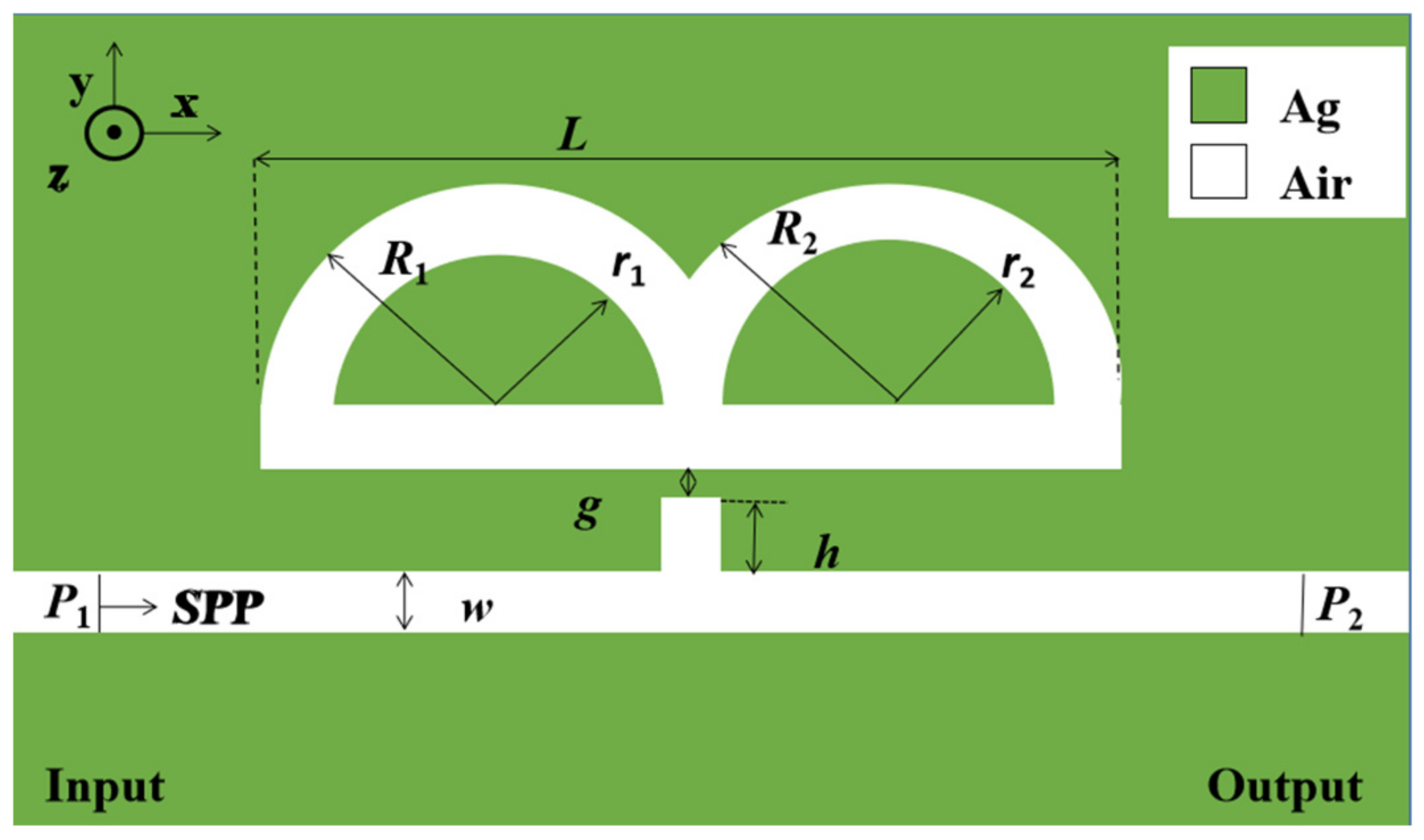
2. Materials and Methods
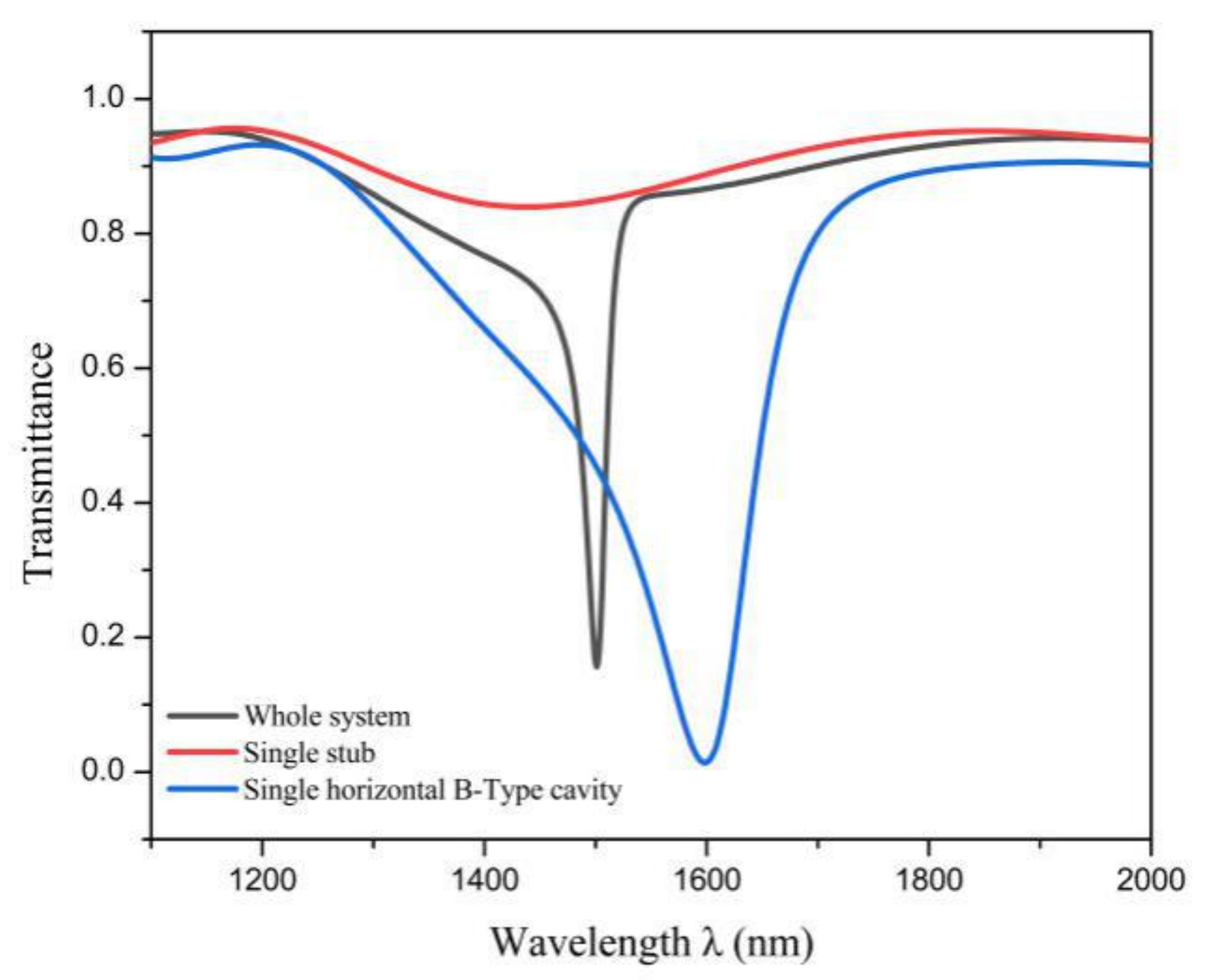
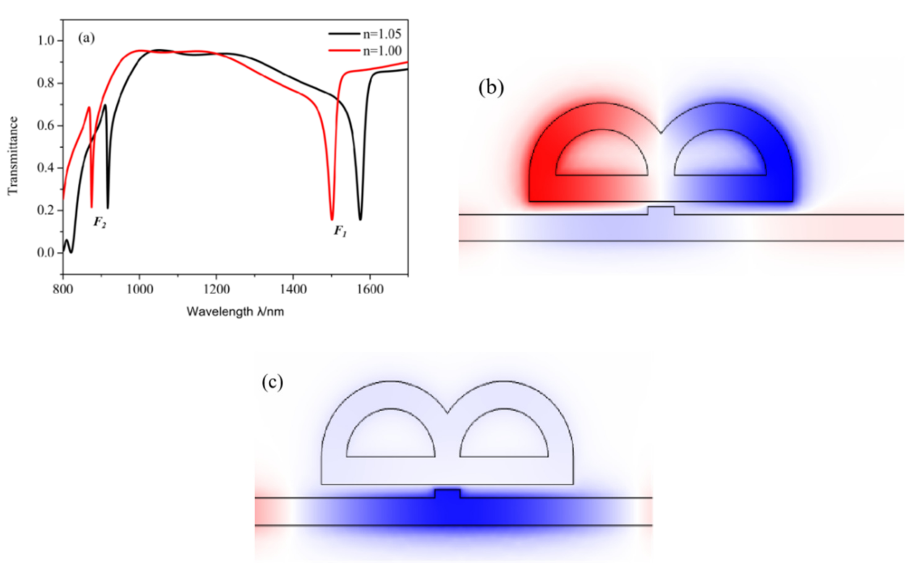
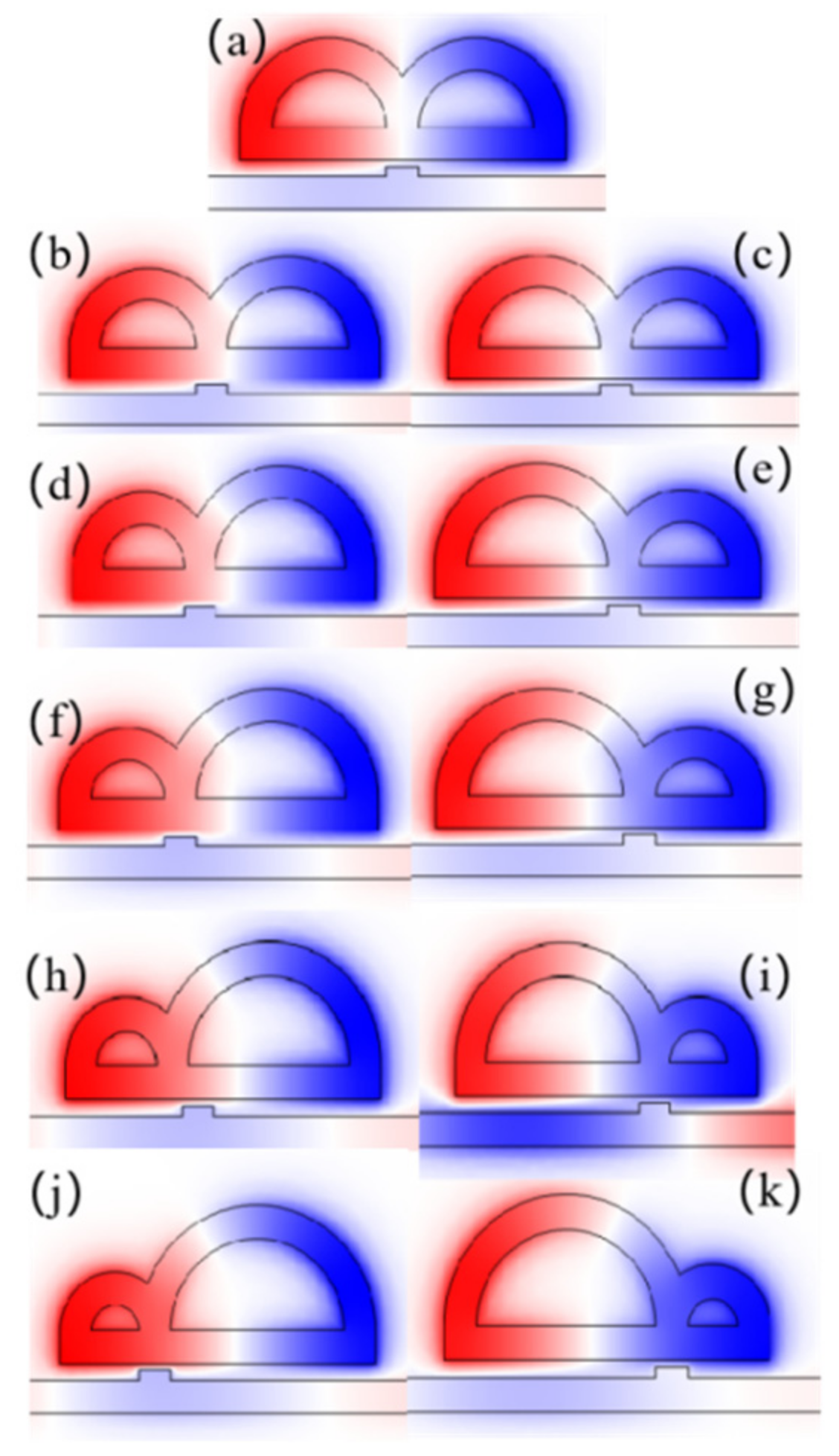
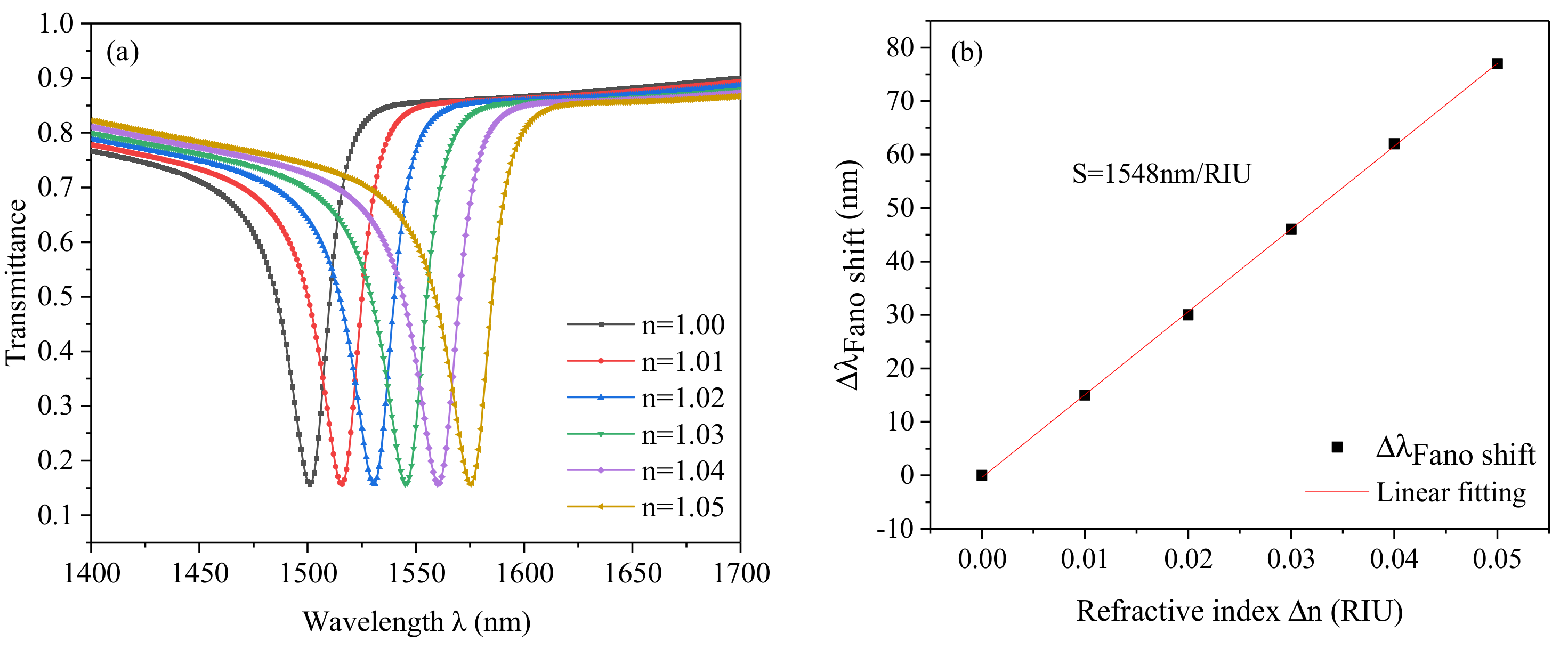
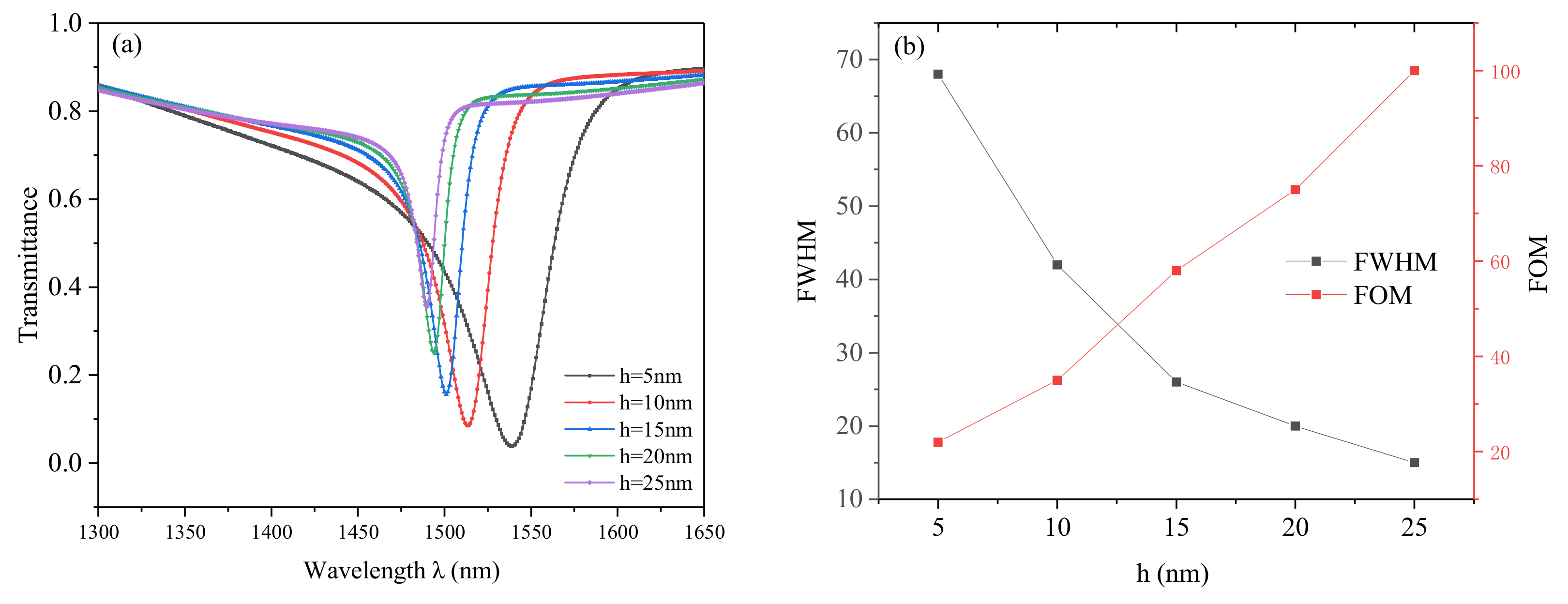
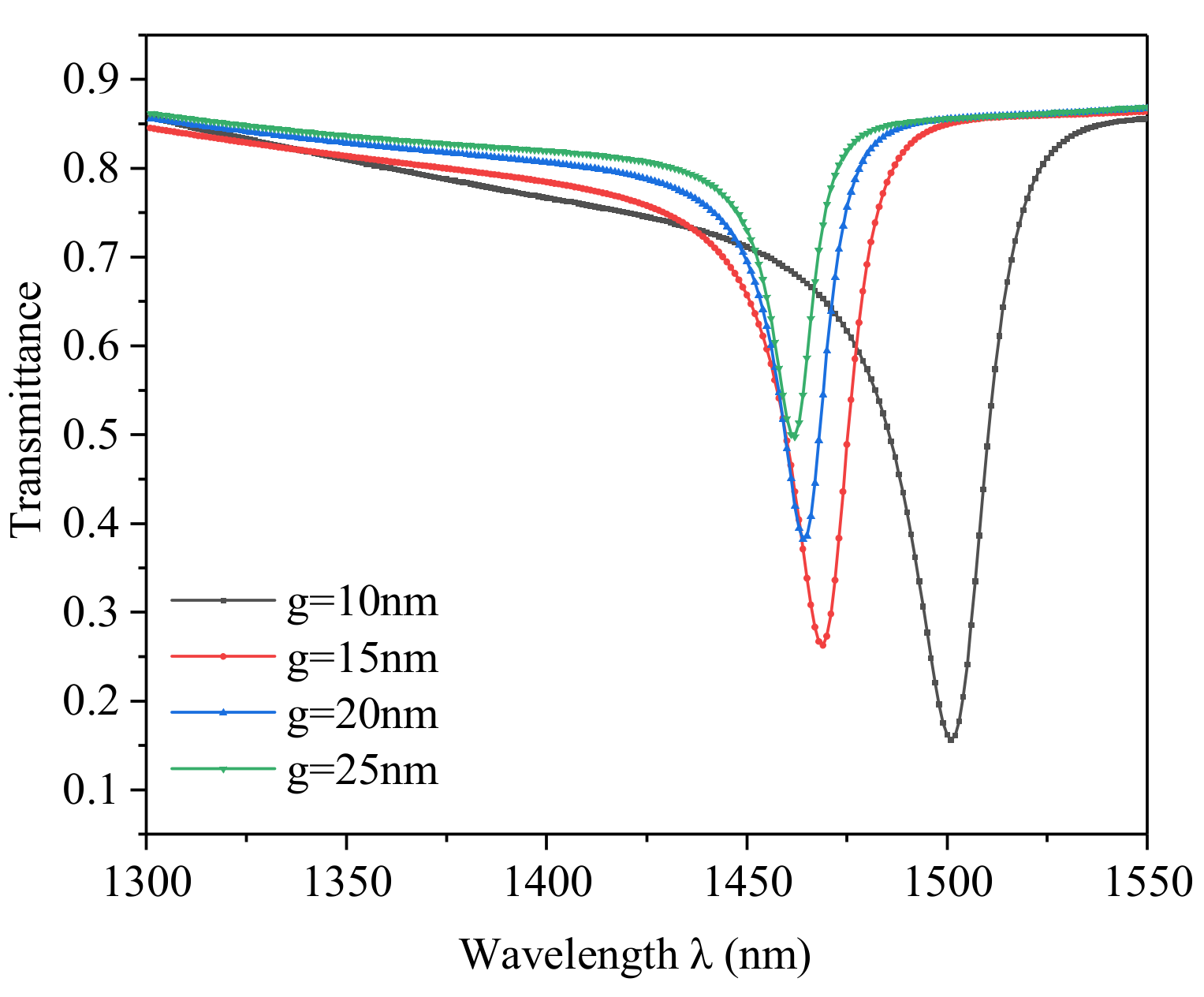
Figure 1 is the geometric structure of the presented design, which consists of a horizontal B-Type cavity coupled with the MIM waveguide with a stub. Here, we use the 2D model to replace the 3D one, which can simplify the calculation. As if the structure height is larger than the skin depth of SPPs (in real photonic devices, the structure height is larger than the skin depth of SPPs), the role of structure height in the losses of the 3D model can be approximated by a 2D model. The green and white parts represent a Ag layer and air ( ε S =1), respectively. The refractive index of the white part will change with the change of surrounding materials. The transmission spectra are performed by the finite element method (FEM) numerically, and the dieletric constant of Ag can be expressed using the Debye–Drude dispersion model:
ε Ag ( ω ) = ε 1 ( ω ) + ε 2 ( ω ) i = 1 ω p 2 τ 2 1 + w 2 τ 2 + ( 1 ω p 2 τ ω ( 1 + w 2 τ 2 ) ) i
where ω, ωp = 1.38 × 10¹⁶ rad/s and τ = 7.35 × 10⁻¹⁵ s represents the angular frequency of the light, the plasma frequency of Ag and the relaxation time, respectively [4,23].
The length of the horizontal B-Type cavity is denoted as L. The outer and inner radii of the semi-circle of the horizontal B-Type cavity are described as R1, R2, and r1, r2. The height of stub is denoted by h. g is defined as the coupling distance. In this study, we set w which stands for the width of the MIM waveguide at 50 nm to ensure only TM0 modes exist in the waveguide. P1 and P2 are the input port and output port, respectively.
The simulation is a good method to study and optimize the SPPs’ structure because their nanosize is difficult to manufacture. The physical model is built by the COMSOL Multiphysics software which can also obtain the transmission spectrum by the FEM. First of all, we need to create a physical field; and what we use here is the electromagnetic wave frequency domain field. Next, we set the parameters and set the selected material. Then, we design the scheme and draw the geometric structure. Furthermore, we configure the parameters of the selected physics field. Finally, we set the boundary conditions and grid for simulation. The perfect matched layer is set as an absorption boundary condition. Moreover, ultra-fine meshing is chosen to realize simulative accuracy. In this design, sub-domains are divided into triangular mesh elements with a fine mesh grid size. At the same time, to approximate an open geometry, we use scattering boundary conditions at the outer edges of the FEM simulation area.

3. Results

To understand the transmission properties of the designed structure, firstly, the whole system, single stub and single horizontal B-Type cavity are compared. We fix initial structural parameters as L = 460 nm, h = 10 nm, R1, R2 = 127.5 nm, r1, r2 = 77.5 nm, g = 10 nm. The results are plotted in Figure 2.
Figure 2 shows that the whole system exhibits an obvious Fano resonance curve. The transmission spectrum of the single stub shows a positive slop and has very high transmittance, so the single stub excites a broad-spectrum resonance mode. The transmission spectrum of the single horizontal B-Type cavity has a Lorentz-like shape, so it excites a narrow spectrum resonance mode. Therefore, the Fano resonance is excited by the interaction between the broad band mode and narrow band mode of the whole system.
The dip of the transmission wavelength which is denoted by the incident wavelength, which ( λ F R ) can be calculated according to the standing wave theory by:
λ F R = 2 L e f f n e f f f φ r e f / π  
n e f f = [ ε Ag + ( k / k 0 ) 2 ] 1 / 2
where Leff is the perimeter of the cavity, φ r e f is the phase shift of SPPs reflection in the cavity, neff is the effective refractive index. Additionally, f is the resonance mode order (f = 1, 2, 3 …) [15]. k and k0 are the wave vector in the waveguide and wave vector in free space and k = β 2 ε Ag k 0 2 , k0 = 2π/λFR, β is the propagation constant [18].
As it is a nanostructure and the working wavelength is about 1600 nm, the material loss must be taken into account. When ω < ω p , the imaginary part of ε A g ( ω ) should be taken into consideration which stands for the absorption loss. The tg( ε ( ω ) ) is the general formula of dielectric loss and, after calculating, it is about 0.08, which is a reasonable value. The skin depth of silver is described as δ A g = λ / ( 4 π ε A g ( ω ) ) which is 10.27 nm in this system. Additionally, this means that the SPPs are bound to the metal surface.
As shown in Figure 3a, we can see two Fano resonance dips in the transmission spectrum, and they are described as F1 and F2. Although the FWHM of F2 is narrower, the sensitivity of F2 obtaining 760 nm/RIU is lower than that of F1 that is 1320 nm/RIU. Therefore, we choose F1 as the object of this study.
In order to further understand the underlying principle of Fano resonance, the HZ filed distributions are studied and plotted in Figure 3b,c. From Figure 3b, the power flow is almost concentrated in the horizontal B-Type cavity and Fano resonance is excited, the reason for which is that destructive interference is induced between the incident SPPs and the SPPs from the stub to the MIM waveguide. From Figure 3c, the power flow is almost concentrated in the MIM waveguide and transmission is enhanced, the reason of which is that constructive interference is induced between the two excitations. According to Equations (1)–(3) and the effective SPPs wavelength, λ SPPs = λ FR / n e f f , when λ FR = 1500 nm, λ SPPs = 1071 nm, ( π ( R 1 + L ) / λ SPPs 1 , which shows that λ SPPs = 990 nm meets the condition of Fano resonance and confirms the simulation result when f = 1.
The S and FOM are important values for a sensor, which are described as:
S = Δ λ Δ n
F O M = S F W H M
where Δ λ is the shift of the resonance wavelength; Δ n is the change of refractive index [8,12].
We then analyze the effects of different similar structures on the transmission spectra and normalized magnetic field HZ. The parameters are all consistent with those in Figure 3, except ΔR = R1R2 which is the difference between R1 and R2. We study the transmission spectra of different structures, whose ΔR are −100, −80, −60, −40, −20, 0, 20, 40, 60, 80 and 100 nm, respectively. As depicted in Figure 4, there are differences among transmittance spectra of these eleven structures (when the absolute values of ΔR are equal, their transmission spectra are similar, the reason for which is that the Leff are same and their structures are symmetrical about the reference line, so we select part of the data for more intuitive representation). Some observable phenomena can be seen in Figure 4: as the absolute value of ΔR increases, the transmittance at their dips becomes lower. However, their FWHM becomes broader, which means obtaining a poorer FOM. At the same time, it can be observed that the position of the dips change, an obvious redshift, when the absolute values of ΔR increase. As for the ΔR = −100 nm, its transmission spectrum is more similar to the Lorentz shape curve, which has the lowest transmittance among these structures but a broad FWHM which leads to a low FOM. It can be concluded that proper destruction of the symmetry of the structure can offer the gain for the generation of Fano resonance, which has better sensing properties of low transmittance. As when ΔR is smaller than −100 nm FOM becomes smaller than that of −100 nm and the trend it presented is not different from the previous groups of experiments, it is meaningless to discuss in this part. Therefore, when ΔR = 0 nm, the structure obtained the narrowest FWHM, which leads to the best FOM of these structures.
Furthermore, the normalized HZ field of these structures is analyzed, as plotted in Figure 5. We can clearly observe in Figure 5 that when the absolute values of ΔR changed, the normalized HZ field of these structures are still symmetrical about the reference line. However, it was obvious that the smaller radius of the structure had a stronger binding ability to the magnetic field and the big one had a wider magnetic field distribution, which also means that the external environment can be detected over a wider range; there was only one node in the ΔR = 0 nm structure, but there were two nodes in the other structures. According to the above analysis, we can understand that we can change ΔR to obtain different transmittance, the wavelength of Fano resonance and the normalized HZ field. Hence, we choose the ΔR = 0 nm structure to study in this paper.
The measuring principle of the plasmonic refractive index sensing structure is that the resonance dip will shift with the changing of the refractive index of surrounding materials. The refractive index n varies from 1.00 RIU to 1.05 RIU in steps of 0.01 RIU, with the default structure parameters L, R1, R2, r1, r2, h and g being set at 500 nm, 137.5 nm, 137.5 nm, 87.5 nm, 87.5 nm, 15 fnm and 10 fnm. In practical applications, the refractive index will change according to the changes to be measured, such as temperature, humidity and liquid concentration, etc. It is obvious in Figure 6a that the transmission spectra show a remarkable redshift with the increasing n. Figure 6a shows that the Fano resonance dip has a nearly linear shift with the change of Δ n . After calculating by the Origin plotted in Figure 6b, the S is 1548 nm/RIU and the FOM becomes 59. The default values are the best structure parameters and the properties is better than most of those that are listed in Table 1.
Subsequently, the effects of geometric parameters of the design on sensing performance are studied. The length of the horizontal B-Type cavity L is discussed first (R1, R2, r1 and r2 will change with it). The values of L change from 420 nm to 500 nm at intervals of 20 nm and other values are set as default values when n = 1, whose results are shown in Figure 7. The resonance dip shows an obvious redshift with increasing L as depicted in Figure 7a which can be explained by Equation (2): when L increases, the propagation length of SPPs in the Fano resonance cavity will increase, which will cause the value of λ F R to increase. Moreover, it is clear that, when L = 420 nm, the resonance curve is more similar to the Lorentz curve. However, with increasing L, the curve of asymmetry degree is increasing, the S of the design will become higher from 1245 to 1548 nm/RIU when L increases from 420 to 500 nm as plotted in Figure 7b. Therefore, The length of the horizontal B-Type cavity L influences not only the position of Fano dip but also S.
Furthermore, we analyze the influence of different h on the transmission properties. We change the values of h from 5 nm to 25 nm in a step of 5 nm and other values are set as default values when n = 1, whose results are shown in Figure 8. The resonance dip shows an obvious blueshift with increasing h as depicted in Figure 8a. Moreover, it is clear that, with increasing h, the FWHM decreases, which means that FOM increases. The FOM of the design increases from 18 to 100 as depicted in Figure 8b. However, when h increases to 25 nm, it can be seen that the transmittance obviously becomes higher, which means that h corresponds to the broad band in this system, and results in weakening the sensing performance. Additionally, the transmittance will become higher, which will mean that the SPPs are difficult to detect, when h is larger than 25 nm. Therefore, we only analyze that h ranges from 5 to 25 nm. Considering this, we set h as 15 nm in this paper.
Finally, we analyze the effects of different coupling distances on sensing properties. The g is set from 5 to 25 nm and the results are plotted in Figure 9. With an increase in g, there is an obvious blueshift and the transmittance becomes higher swiftly, which means that the confinement of the cavity to energy becomes weaker. Additionally, the attenuation distance is δ A i r = λ ε A g ( ω ) / ( 4 π ε S ) = 1579 nm longer than the coupling distance. Therefore, we can infer that SPPs from the stub can be coupled into the athletic track cavity theoretically. According to this result, we can apply it to the pressure sensor mentioned in the introduction, which will be a good application.
The focused ion beam method is used to manufacture this structure. The specific operation is that the focused ion beam is sputtered on the Ag film (the thickness of Ag is about 100 nm) above the quartz substrate. Then, the nanostructure is patterned by controlling the position of the focused ion beam. With the continuous advancement of material science and MEMS (Micro-Electro-Mechanical System) processing technology, the nanosenseor based on Fano resonance will be manufactured and used in real life.

4. Conclusions

In this article, we propose a plamonic nanosensor based on a metal–insulator–metal waveguide with a stub coupling with a horizontal B-Type cavity. The transmission properties of the design are investigated on COMSOL by using the FEM. The optimal geometrical parameters L, R1, R2, r1, r2, h and g are at 500 nm, 137.5 nm, 137.5 nm, 87.5 nm, 87.5 nm, 15 nm and 10 nm, whose sensitivity and FOM are 1548 nm/RIU and 59, respectively. The normalized HZ field is affected by the difference value between the R1 and R2 greatly. The sensing performance can be controlled by adjusting the geometric parameters. R1, R2, r1, r2 and L can adjust the sensitivity largely. The ΔR and h are the key to controlling the lineshape and the FOM. The simple sensing structure we have proposed offers a better choice for nanosensing.

Author Contributions

Conceptualization, S.Y. and H.S.; methodology, X.Y.; software, H.S.; formal analysis, S.Y.; investigation, W.W.; resources, E.H.; data curation, J.G.; writing—original draft preparation, H.S.; writing—review and editing, H.S. and S.Y.; supervision, H.S.; project administration, S.Y.; funding acquisition, S.Y., H.S. and S.Y. contributed equally to this work. All authors have read and agreed to the published version of the manuscript.

Funding

This research was funded in part by the National Natural Science Foundation of China under Grant 61675185, Grant 61875250, and Grant 61975189; in part by the Natural Science Foundation of Zhejiang Province under Grant LD21F050001; in part by the Key Research and Development Project of Zhejiang Province under Grant 2021C03019; and in part by the Fund for Shanxi 1331Project Key Subject Construction.

Informed Consent Statement

Informed consent was obtained from all subjects involved in the study.

Data Availability Statement

The available data has been stated in the article.

Acknowledgments

System numerical simulation was provided by COMSOL, INC.

Conflicts of Interest

The authors declare no conflict of interest.

References

  1. Shi, X.; Ma, L.; Zhang, Z.; Tang, Y.; Zhang, Y.; Han, J.; Sun, Y. Dual Fano resonance control and refractive index sensors based on a plasmonic waveguide-coupled resonator system. Opt. Commun. 2018, 427, 326–330. [Google Scholar] [CrossRef]
  2. Tavakoli, F.; Ebrahimi, S. Planar optical waveguide for refractive index determining with high sensitivity and dual-band characteristic for Nano-sensor application. Opt. Quantum Electron. 2019, 51, 185. [Google Scholar] [CrossRef]
  3. Qi, Y.P.; Wang, L.Y.; Zhang, Y.; Zhang, T.; Zhang, B.H.; Deng, X.Y.; Wang, X.X. Multiple Fano resonances in metal-insulator-metal waveguide with umbrella resonator coupled with metal baffle for refractive index sensing. Chin. Phys. B 2020, 29, 067303. [Google Scholar] [CrossRef]
  4. Bazgir, M.; Jalalpour, M.; Zarrabi, F.B.; Arezoomand, A.S. Design of an optical switch and sensor based on a MIM coupled waveguide using a DNA composite. J. Electron. Mater. 2020, 49, 2173–2178. [Google Scholar] [CrossRef]
  5. Barnes, W.L.; Dereux, A.; Ebbesen, T.W. Surface plasmon subwavelength optics. Nature 2003, 424, 824–830. [Google Scholar] [CrossRef]
  6. Haddouche, I.; Lynda, C. Comparison of finite element and transfer matrix methods for numerical investigation of surface plasmon waveguides. Opt. Common. 2017, 382, 132–137. [Google Scholar] [CrossRef]
  7. Fang, Y.; Sun, M. Nanoplasmonic waveguides: Towards applications in integrated nanophotonic circuits. Light Sci. Appl. 2015, 4, e294. [Google Scholar] [CrossRef] [Green Version]
  8. Nehl, C.L.; Liao, H.; Hafner, J.H. Optical properties of star-shaped gold nanoparticles. Nano Lett. 2006, 6, 683–688. [Google Scholar] [CrossRef] [Green Version]
  9. Kato, N.; Lee, L.; Chandrawati, R.; Johnston, A.P.; Caruso, F. Optically Characterized DNA Multilayered Assemblies and Phenomenological Modeling of Layer-by-Layer Hybridization. J. Phys. Chem. C 2009, 113, 21185–21195. [Google Scholar] [CrossRef]
  10. Yang, X.D.; Liu, Y.; Oulton, R.F.; Yin, X.; Zhang, X. Optical forces in hybrid plasmonic waveguides. Nano Lett. 2011, 11, 321–328. [Google Scholar] [CrossRef]
  11. Wang, S.; Li, Y.; Xu, Q.; Li, S. A MIM Filter Based on a Side-Coupled Crossbeam Square-Ring Resonator. Plasmonics 2016, 11, 1291–1296. [Google Scholar] [CrossRef]
  12. Tong, L.; Wei, H.; Zhang, S.; Xu, H. Recent Advances in Plasmonic Sensors. Sensors 2014, 14, 7959–7973. [Google Scholar] [CrossRef] [PubMed] [Green Version]
  13. Sarkaleh, A.K.; Lahijani, B.V.; Saberkari, H.; Esmaeeli, A. Optical Ring Resonators: A Platform for Biological Sensing Applications. J. Med. Signals Sens. 2017, 7, 185–191. [Google Scholar] [CrossRef] [PubMed]
  14. Tsigaridas, G.N. A study on refractive index sensors based on optical micro-ring resonators. Photonic Sens. 2017, 7, 217–225. [Google Scholar] [CrossRef]
  15. Ma, F.; Lee, C. Optical Nanofilters Based on Meta-Atom Side-Coupled Plasmonics Metal-Insulator-Metal Waveguides. J. Lightwave Technol. 2013, 31, 2876–2880. [Google Scholar] [CrossRef] [Green Version]
  16. Veronis, G.; Fan, S. Bends and splitters in metal-dielectric-metal subwavelength plasmonic waveguides. Appl. Phys. Lett. 2005, 87, 131102. [Google Scholar] [CrossRef]
  17. Zhang, Z.-D.; Wang, H.-Y.; Zhang, Z.-Y. Fano resonance in a gear-shaped nanocavity of the metal–insulator–metal waveguide. Plasmonics 2013, 8, 797–801. [Google Scholar] [CrossRef]
  18. Piao, X.; Yu, S.; Koo, S.; Lee, K.; Park, N. Fano-type spectral asymmetry and its control for plasmonic metal-insulator-metal stub structures. Opt. Express 2011, 19, 10907–10912. [Google Scholar] [CrossRef]
  19. Zhang, Z.; Shi, F.; Chen, Y. Tunable Multichannel Plasmonic Filter Based on Coupling-Induced Mode Splitting. Plasmonics 2015, 10, 139–144. [Google Scholar] [CrossRef]
  20. Ni, B.; Chen, X.Y.; Xiong, D.Y.; Liu, H.; Hua, G.H.; Chang, J.H.; Zhou, H. Infrared plasmonic refractive index-sensitive nanosensor based on electromagnetically induced transparency of waveguide resonator systems. Opt. Quantum Electron. 2015, 47, 1339–1346. [Google Scholar] [CrossRef]
  21. Kirchain, R.; Kimerling, L. A roadmap for nanophotonics. Nat. Photonics 2007, 1, 303–305. [Google Scholar] [CrossRef]
  22. Abbas, M.N.; Cheng, C.W.; Chang, Y.C.; Shih, M.H. An omni-directional mid-infrared tunable plasmonic polarization filter. Nanotechnology 2012, 23, 444007. [Google Scholar] [CrossRef] [PubMed]
  23. Yang, Y.M.; Kelley, K.; Sachet, E.; Campione, S.; Luk, T.S.; Maria, J.-P.; Sinclair, M.B.; Brener, I. Femtosecond optical polarization switching using a cadmium oxide-based perfect absorber. Nat. Photonics 2017, 11, 390. [Google Scholar] [CrossRef]
  24. Kuttruff, J.; Garoli, D.; Allerbeck, J.; Krahne, R.; De Luca, A.; Brida, D.; Caligiuri, V.; Maccaferri, N. Ultrafast all-optical switching enabled by epsilon-near-zero-tailored absorption in metal-insulator nanocavities. Commun. Phys. 2020, 3, 114. [Google Scholar] [CrossRef]
  25. Wu, J.; Lang, P.; Chen, X.; Zhang, R. A novel optical pressure sensor based on surface plasmon polariton resonator. J. Mod. Opt. 2016, 63, 219–223. [Google Scholar] [CrossRef]
  26. Carrara, A.; Maccaferri, N.; Cerea, A.; Bozzola, A.; De Angelis, F.; Zaccaria, R.P.; Toma, A. Plasmon Hybridization in Compressible Metal-Insulator-Metal Nanocavities: An Optical Approach for Sensing Deep Sub-Wavelength Deformation. Adv. Opt. Mater. 2020, 8. [Google Scholar] [CrossRef]
  27. Chen, J.F.; Li, J.; Liu, X.; Rohimah, S.; Tian, H.; Qi, D. Fano resonance in a MIM waveguide with double symmetric rectangular stubs and its sensing characteristics. Opt. Commun. 2021, 482, 126563. [Google Scholar] [CrossRef]
  28. Qi, Y.; Zhang, T.; Zhang, Y.; Wang, X. Tunable sharp resonances based on multimode interference in a MIM-ring coupling plasmonic resonator system. Epl 2020, 132, 132. [Google Scholar] [CrossRef]
  29. Yang, Q.; Liu, X.; Guo, F.; Bai, H.; Zhang, B.; Li, X.; Tan, Y.; Zhang, Z. Multiple Fano resonance in MIM waveguide system with cross-shaped cavity. Optik 2020, 220, 165163. [Google Scholar] [CrossRef]
  30. Wang, S.; Yu, S.; Zhao, T.; Wang, Y.; Shi, X. A nanosensor with ultra-high FOM based on tunable malleable multiple Fano resonances in a waveguide coupled isosceles triangular resonator. Opt. Commun. 2020, 465, 125614. [Google Scholar] [CrossRef]
  31. Zhu, J.; Li, N. MIM waveguide structure consisting of a semicircular resonant cavity coupled with a key-shaped resonant cavity. Opt. Express 2020, 28, 19978–19987. [Google Scholar] [CrossRef]
  32. Rahmatiyar, M.; Afsahi, M.; Danaie, M. Design of a Refractive Index Plasmonic Sensor Based on a Ring Resonator Coupled to a MIM Waveguide Containing Tapered Defects. Plasmonics 2020, 15, 2169–2176. [Google Scholar] [CrossRef]
  33. Chen, Y.; Xu, Y.M.; Cao, J.G. Fano resonance sensing characteristics of MIM waveguide coupled Square Convex Ring Resonator with metallic baffle. Results Phys. 2019, 14. [Google Scholar] [CrossRef]
  34. Butt, M.A.; Kazanskiy, N.L.; Khonina, S.N. Highly integrated plasmonic sensor design for the simultaneous detection of multiple analytes. Curr. Appl. Phys. 2020, 20, 1274–1280. [Google Scholar] [CrossRef]
  35. Chao, C.T.C.; Chau, Y.-F.C.; Huang, H.J.; Kumara, N.T.R.N.; Kooh, M.R.R.; Lim, C.M.; Chiang, H.-P. Highly Sensitive and Tunable Plasmonic Sensor Based on a Nanoring Resonator with Silver Nanorods. Nanomaterials 2020, 10, 1399. [Google Scholar] [CrossRef]
  36. Sreekanth, K.V.; Alapan, Y.; ElKabbash, M.; Ilker, E.; Hinczewski, M.; Gurkan, U.A.; De Luca, A.; Strangi, G. Extreme sensitivity biosensing platform based on hyperbolic metamaterials. Nat. Mater. 2016, 15, 621–627. [Google Scholar] [CrossRef] [Green Version]
Figure 1. The geometric structure of the coupled the horizontal B-Type cavity.
Photonics 08 00125 g001
Figure 2. Transmission spectra of the whole system, the single stub and horizontal B-Type cavity.
Photonics 08 00125 g002
Figure 3. (a) Transmission spectrum of the system; (b,c) the magnetic field distribution HZ at λ = 1500 and 2000 nm.
Photonics 08 00125 g003
Figure 4. Transmission spectra of different ΔR.
Photonics 08 00125 g004
Figure 5. The magnetic field distribution HZ at the Fano resonance dip of (a) ΔR = 0 nm at λ = 1500 nm; (b,c) ΔR = −20 and 20 nm at λ = 1502 nm; (d,e) ΔR = −40 and 40 nm at λ = 1506 nm; (f,g) ΔR = −60 and 60 nm at λ = 1512 nm; (h,i) ΔR = −180 and 180 nm at λ = 1515 nm; (j,k) ΔR = −100 and 100 nm at λ = 1530 nm.
Photonics 08 00125 g005
Figure 6. (a) Transmission spectra of the refractive indices n ranging from 1.00 to 1.05 RIU. (b) Linear fitting of the sensitivity.
Photonics 08 00125 g006
Figure 7. (a) Transmission spectra of the different length of the horizontal B-Type cavity L; (b) linear fitting of the sensitivity.
Photonics 08 00125 g007
Figure 8. (a) Transmission spectra of h varying from 5 to 25 nm; (b) the tendency of full width at half maximum (FWHM) and figure of merit (FOM) with increasing h.
Photonics 08 00125 g008
Figure 9. Transmission spectra of different coupling distance g.
Photonics 08 00125 g009
Table 1. Comparisons of results with other previous research.
ReferenceSensitivity (nm/RIU)ReferenceSensitivity (nm/RIU)
This paper1548[31]1262
[27]1180[32]1295
[28]1350[33]1120
[29]1075[34]1949
[30]1200[35]2080
Publisher’s Note: MDPI stays neutral with regard to jurisdictional claims in published maps and institutional affiliations.

