1. Introduction
The enticing prospect of concentrating and controlling light at a sub-wavelength scale has inspired tremendous interest in the field of plasmonics [
1]. Different waveguide [
2] and metamaterial [
3,
4] geometries have been explored to develop nano antennas [
5], optical interconnects [
6], super-resolution imaging [
7], and different sensing devices [
8]. Over the last few decades, steady progress has been made in the development of biosensors in diagnostic, enzyme detection, and food safety, and of gas sensors in industrial safety [
1,
9,
10]. Since its first demonstration by Jorgenson et al., surface plasmon resonance in conjunction with optical fibers has given birth to a new era in the field of sensing [
1].
Surface plasmons are the collective oscillation of the free electrons at the metal dielectric interface, leading to the generation of a resonant electric field that decays in a transverse direction exponentially in both of the media [
11]. Two configurations have been reported in the literature for the excitation of the surface plasmons—the Kretschmann configuration and the Otto configuration. Out of these two, the Kretschmann configuration is easy to implement. In the Kretschmann configuration, SPR interrogation is performed with either of the following two methods: wavelength interrogation or angular interrogation. In the wavelength interrogation method, the angle of incidence of the exciting light is kept fixed and the wavelength is varied to excite the SPR, while in the angular interrogation method, the wavelength of the exciting light is fixed and the angle of incidence is varied. In the Kretschmann configuration, the metal strip is deposited on the base of the prism and p-polarized light is launch at the metal-prism interface from one of the faces of the prism at an angle greater than the critical angle, and reflected light is detected from the other face. The dielectric medium to be sensed is kept in contact with the metal film at the prism base. The incident light after suffering total internal reflection generates an evanescent wave at the metal dielectric interface, which passes through the metal film and excites the surface plasmons at the metal-dielectric interface, resulting in the transfer of energy to the Surface Plasmon Wave (SPW). We observed that, for a particular incident angle, the reflectivity of the curve, measured at the other face of the prism, becomes minimum. This angle is known as the resonance angle, and at this particular angle, the propagation constants of the evanescent wave and the surface plasmon wave becomes equal. The resonance angle depends on the refractive index (RI) of the outer dielectric medium, which is kept in contact with the gold layer.
Once the gold layer is activated properly, the phenomenon of surface plasmon resonance can be used for the detection of different gases and biomolecules. When the sample containing biomolecules or gas molecules comes into contact with the metal surface, the biomolecules is adsorbed, whereas the gas molecules reacts with metal film and change the ambient RI, which gets reflected in terms of the shift in SPR (reflection) spectrum. Performance of the sensor depends largely on the absorbance of the gas or biomolecules. Hence, the nature of the gas and biomolecules very much affect the sensor’s performance. Recently, graphene has emerged as another material with an important property of high sensitivity towards different gases and bio-molecules. Graphene shows very good mechanical, electrical, and optical properties, which has attracted many researchers and scientists in different areas of research. Graphene, having zero bandgap, high electron mobility, very low resistivity, and a 2D structure, opens a new window into the field of sensing [
12].
In the present work, we have carried out a detailed theoretical analysis of a couple of prism-based SPR sensors in the Kretschmann configuration. The prism is made up of GaP material, with a base coated with Au. On top of the Au layer, there is a thin film of graphene, and over that a silicon layer is considered. Silicon has been used to enhance the field and therefore overall sensitivity of the device [
13]. GaP is a transparent semiconductor material with a refractive index of approximately 3.3 in the visible range of the spectrum. Additionally, it is a wide band gap material [
14]. To excite SPs, the angular interrogation technique is utilized using light in the visible region of 632 nm. In our numerical simulation, the thicknesses of the different layers have been optimized to maximize sensitivity in both the gas and bio-sensing schemes. The study reveals that the proposed configuration for a particular numbers of the graphene layers shows very high sensitivity towards bio-materials, while at other thickness its sensitivity towards gas sensing is high. We have also given a comparative analysis of our results for the GaP/Au/Graphene configuration, i.e., without a silicon layer coated sensor.
2. Basic Theory
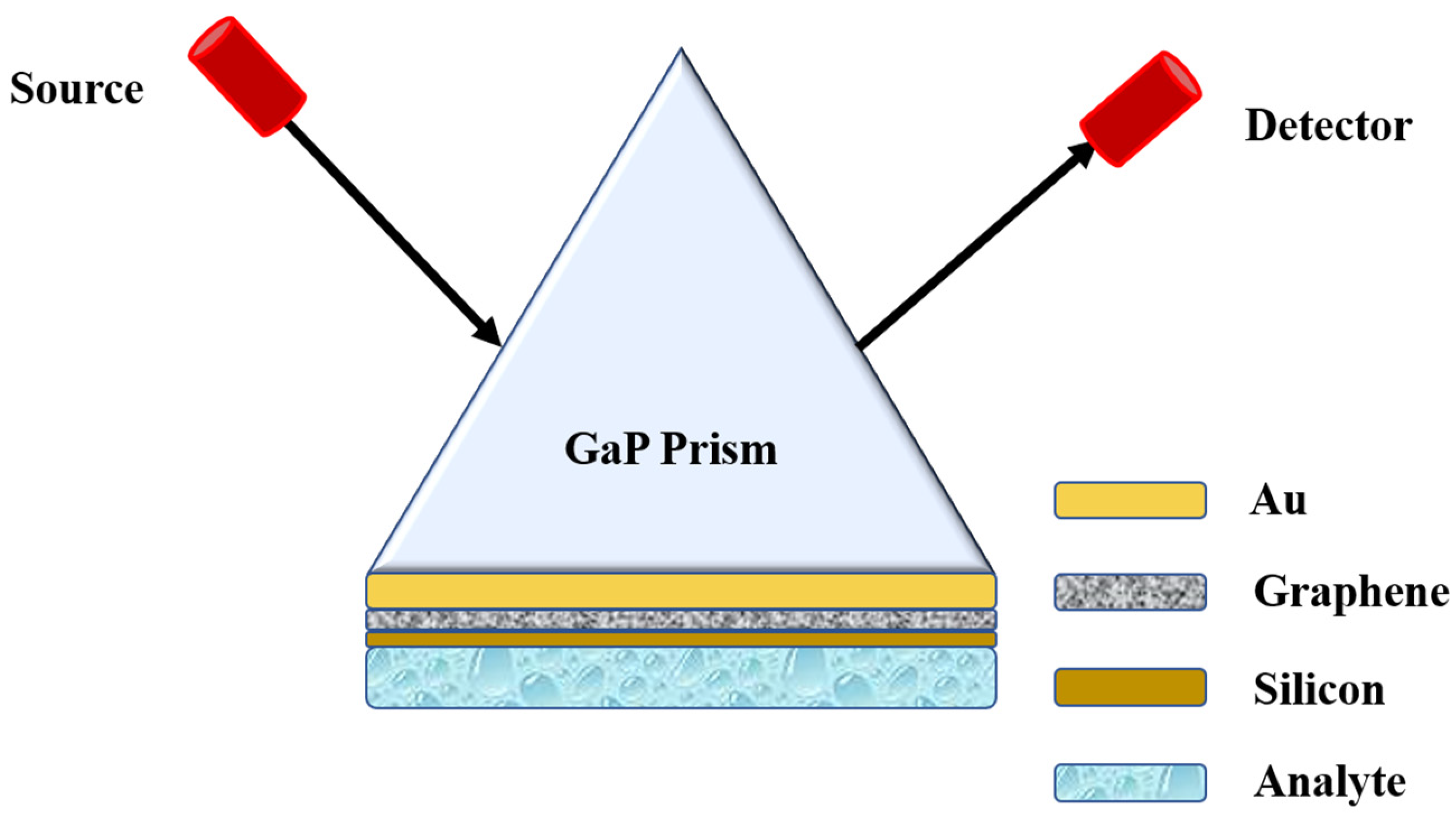
If we consider a prism of GaP, the base of the prism is coated with Au film, which is then followed with the graphene and then the silicon layers. The sensing medium (gases and biomolecules) is considered to be in contact with this sensing probe. A schematic diagram of the proposed probe is shown in
Figure 1. A somewhat different configuration is studied in [
14]. TM-polarized monochromatic light of wavelength 632 nm from a He-Ne laser is made to incident from one face of the prism, and the reflected light is observed from the other face. Because the angular interrogation method is considered, the angle of incidence is varied to achieve phase matching to excite the SPW. At resonance angle, the light is maximally coupled to the surface plasmons, and reflectance shows a corresponding minimum. The position of the reflectance minimum sensitively depends on the sensing medium RI and changes accordingly. For numerical modeling of the proposed probe, the following mathematical relations and parameters are used.
At the given wavelength, the RI of the GaP prism is 3.3 [
15] and that of the Silicon is 3.8354 +
i 0.0245;
i stands for iota [
13]. The RI of Gold is calculated from the following dispersion relation [
16]:
where
and
. The dispersion relation of graphene is given as [
17].
where C is a constant having a value of 0.005446 nm
−1, and the wavelength is measured in nm. As graphene is a two-dimensional structure with a sheet thickness of 0.34 nm, its total thickness depends on the total number of layers (L), deposited and calculated as 0.34 * L nm.
For numerical modelling, the N-layer matrix method has been used [
18,
19]. The characteristic matrix of the N-layer structure can be expressed by:
where
and
, respectively, where
and
are the complex values of the RI and the permittivity of the
layer with thickness
. The reflection coefficient,
, of the p-polarized incident wave can be expressed as:
and therefore the reflectance
is
.
In the vs. plot, the angle associated with minimum corresponds to resonance angle ().
To evaluate the performance of the sensor, we use sensitivity and detection accuracy (DA) as characterizing parameters, which are defined, respectively, as-
Sensitivity: If, for the change in the RI of the sensing medium by
, the corresponding change in the position of the transmission minima angle is
, then the sensitivity is defined as [
20,
21,
22].
The unit of the sensitivity in the angular interrogation method is degree/RIU, while in the wavelength interrogation method it is nm/RIU or µm/RIU. Note that RIU stands for Reftactive Index Unit.
Detection accuracy: DA is defined as the full width at half maximum of the SPR curve [
20,
21,
22].
3. Results
In this study, we have analyzed the two configurations Au/graphene/silicon and Au/graphene using a GaP prism as a substrate. We have studied gas and biomolecule sensing using the same configurations. For the gas sensing, the RI of the gaseous medium are taken to be 1 RIU and 1.0008 RIU, because most of the gases have an RI close to 1. The position of the dip in the reflectance spectra changes with the adsorption of the gas molecules at the uppermost layer. The optimized thickness of the Au layer in the present configuration is found to be 50 nm [
14]. To optimize the design further, sensitivity was calculated for a varying number of graphene layers (L) and for different thicknesses of silicon layer.
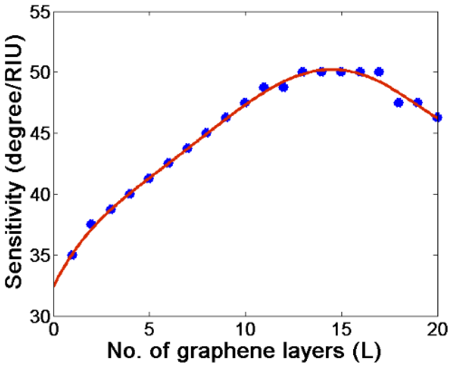
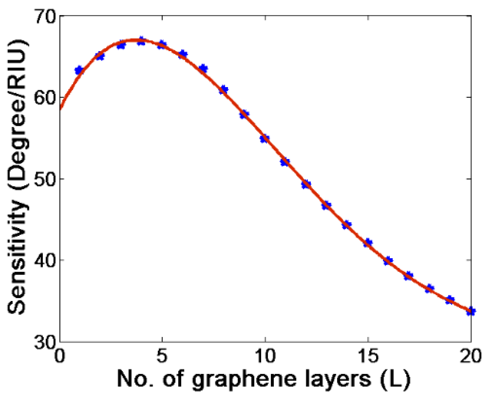
In
Figure 2, we have plotted the sensitivity versus the number of graphene layers deposited over the Au coated GaP prism. To start with, the silicon layer thickness is taken to be 11 nm. It is observed that, as we increase the number of graphene layers, the sensitivity of the sensor increases up to a particular number of graphene layers and then it saturates for a certain range of graphene thicknesses (L = 13 to 17), and afterwards it decreases. We chose 13 layers of graphene as the optimum number for our design. Note that using thermal evaporation or sputtering coating machines, we can deposit silicon layers at a nm level thickness [
19,
23]. Normally, a thickness monitor equipment unit is attached to this coating machine, which accurately measures the layer thickness.
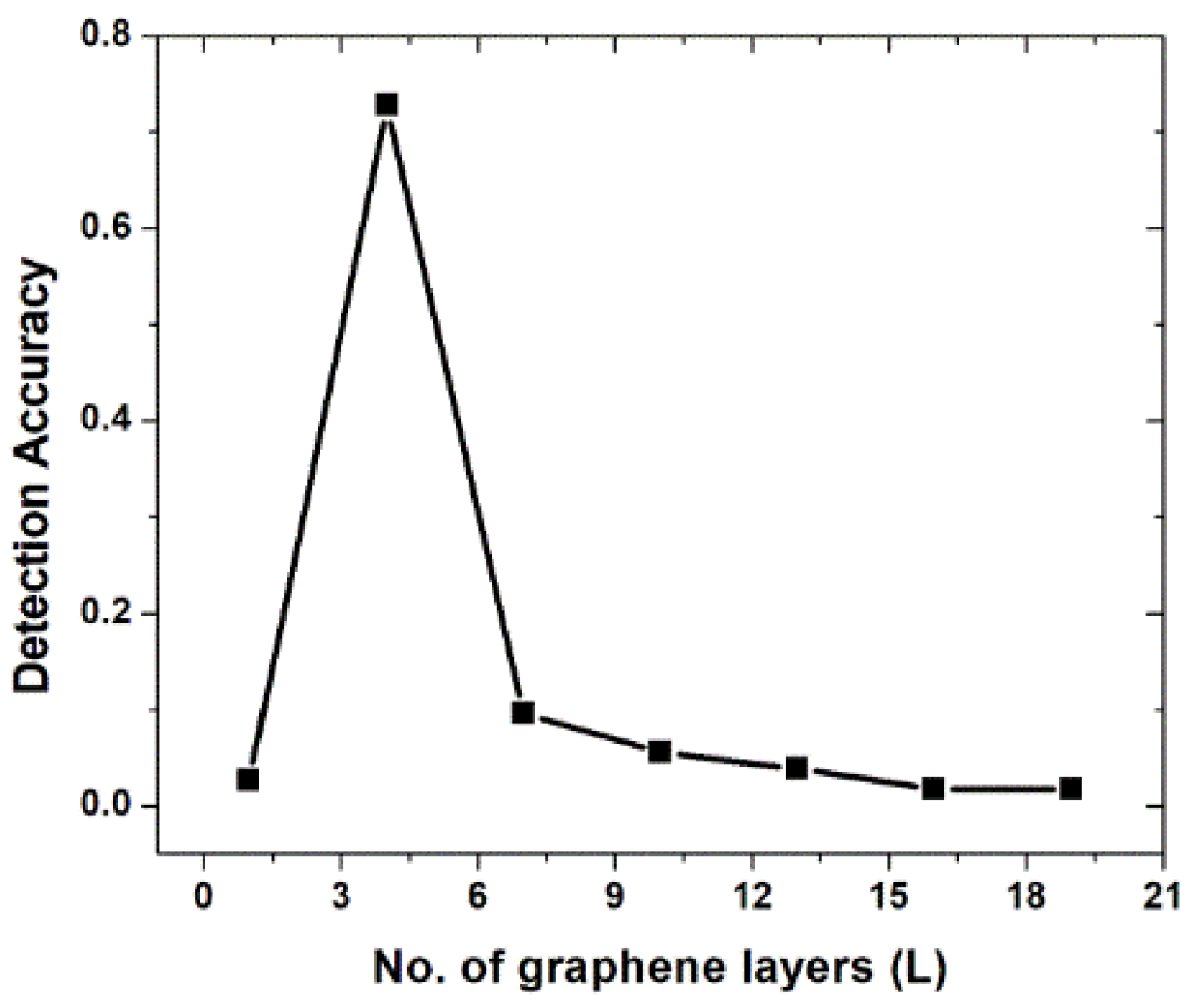
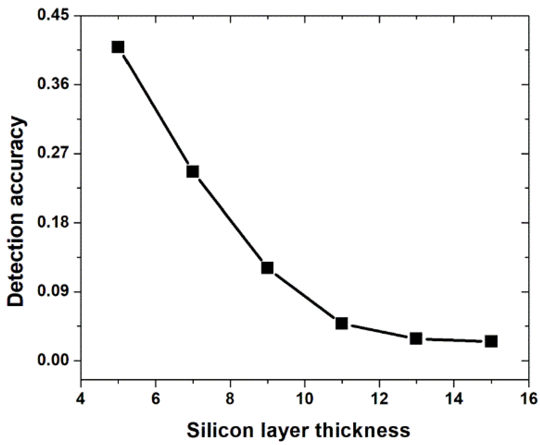
Because graphene is a lossy material, it should decrease the DA of the probe, as observed in
Figure 3. The DA is optimal for four layers of graphene. The simulations for DA calculations were performed for an analyte refractive index of 1 RIU.
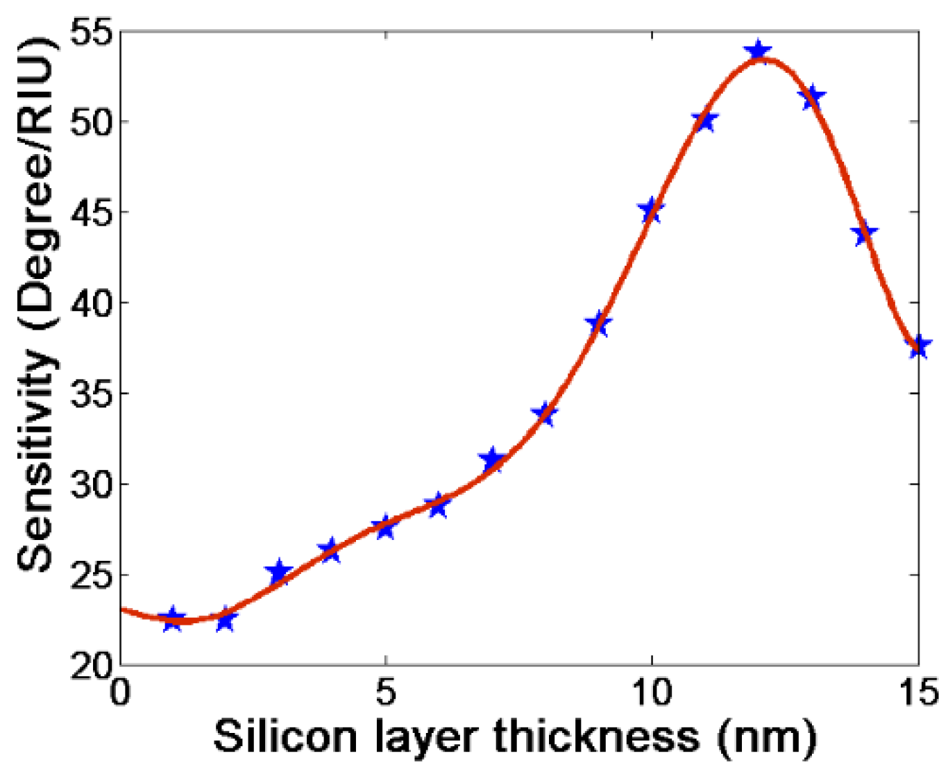
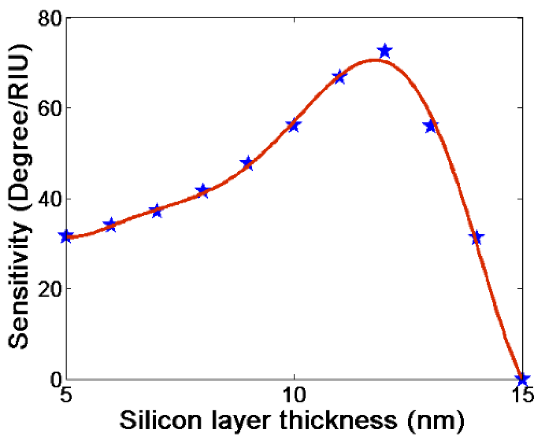
To optimize the thickness of the silicon layer, we fixed the thickness of the Au layer at 50 nm, used the optimized 13 layers of graphene, and varied the thickness of the silicon to see the sensitivity variation in
Figure 4. The maximum sensitivity of 53.75 degree/RIU is observed for a 12 nm thickness of silicon. Thus, the optimized design for gas sensing is Au (50 nm)/graphene (13 layers)/silicon (12 nm), with a sensitivity of 53.75 degree/RIU.
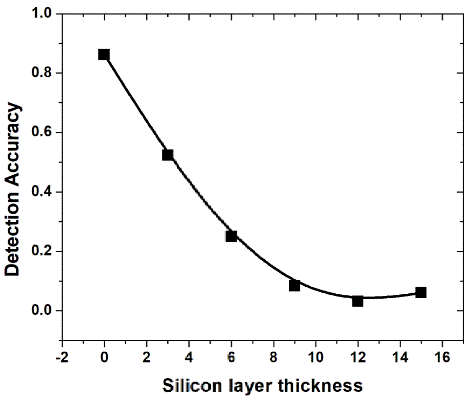
We also studied the DA variation in the above design, as shown in
Figure 5. Because silicon is a lossy dielectric material, DA decreases with the increasing thickness of the silicon. We would like to note that the simulations were performed for gaseous medium refractive index 1 RIU.
To have a comparative study, we have also studied the above sensor without the silicon layer, as shown in
Figure 6. The maximum sensitivity for gas sensing in this case is observed to be 33.75 degree/RIU, which is significantly lower than the previously reported value. This establishes the role of the silicon layer as a sensitivity enhancing layer.
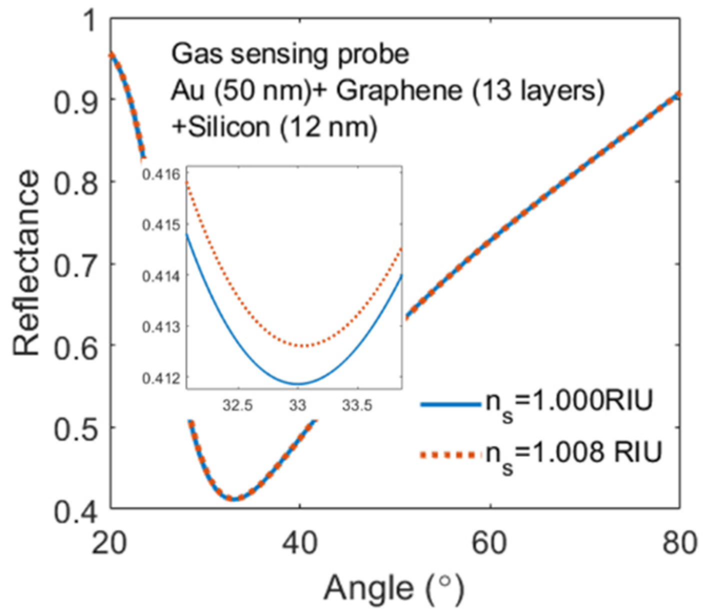
The SPR curve for the optimized gas sensing probe is shown in
Figure 7. We have plotted SPR curves for two refractive indices—1 RIU and 1.008 RIU.
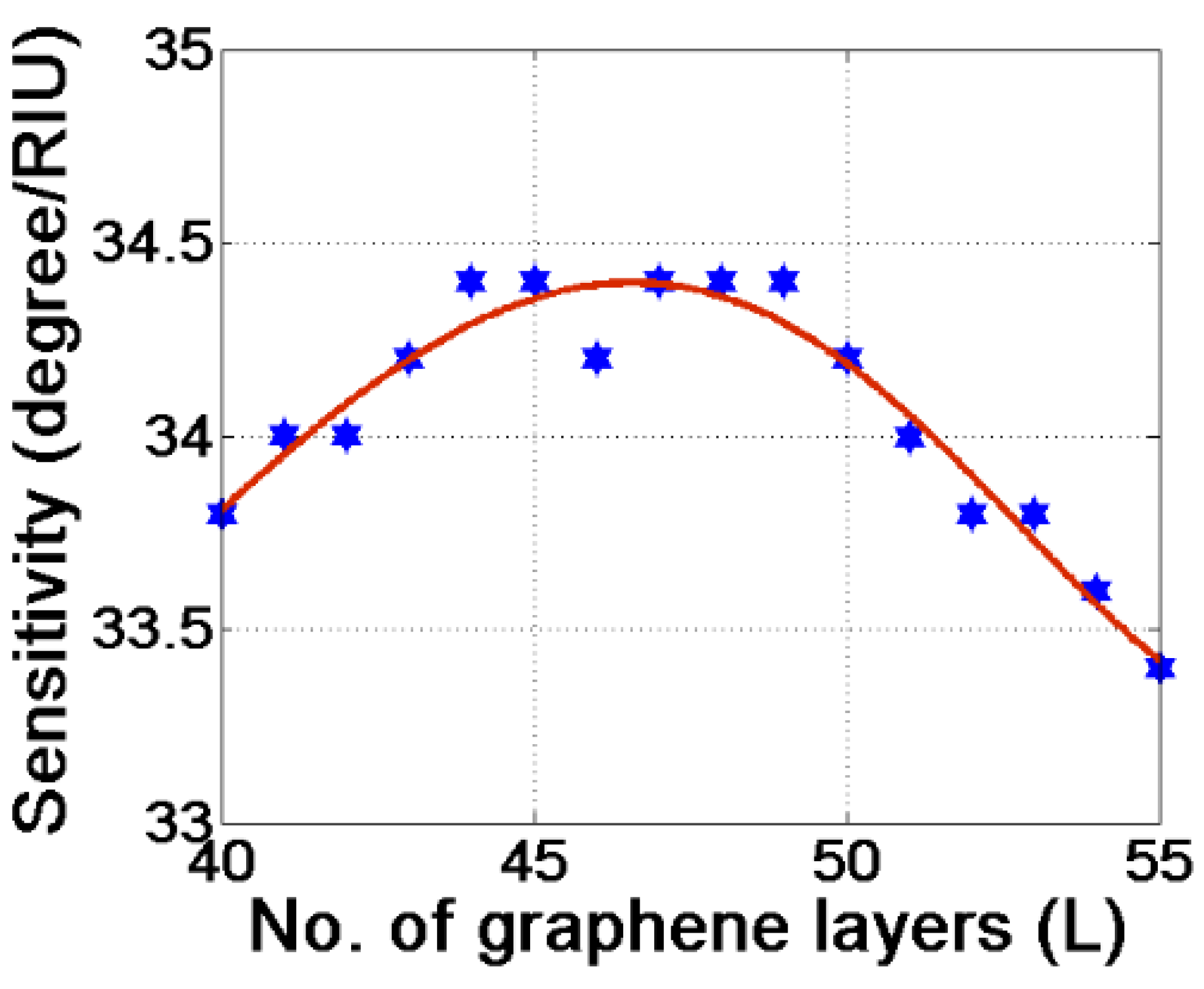
In the following, we have theoretically analyzed the bio sensing performance on the above proposed probe design, but with differently optimized constituent layer thicknesses. For biosensing, we have chosen the RI of the sensing medium, 1.330 RIU, and in the presence of bio-molecules such as bacteria, enzyme, drugs, etc., the sensing medium RI is assumed to shift to 1.335 RIU. To evaluate the sensor performance and to optimize its design, we calculated the sensitivity with 50 nm of Au, varying no. of layers of graphene, and a representative 11 nm thickness of silicon, as depicted in
Figure 8. The figure reveals that the maximum sensitivity of the probe towards the bio sample is 66.80 degree/RIU for four layers of the graphene.
To see the optimized thickness of the silicon layer in the above design, we varied the silicon layer thickness, keeping the Au thickness fixed at 50 nm and no. of graphene layers fixed at four.
Figure 9 shows the sensitivity plot for the same and predicts the optimum thickness of the silicon layer to be 12 nm, and the corresponding sensitivity is 72.60 degree/RIU.
Figure 10 shows the corresponding DA plot. We have performed simulation for refractive index 1.33 RIU.
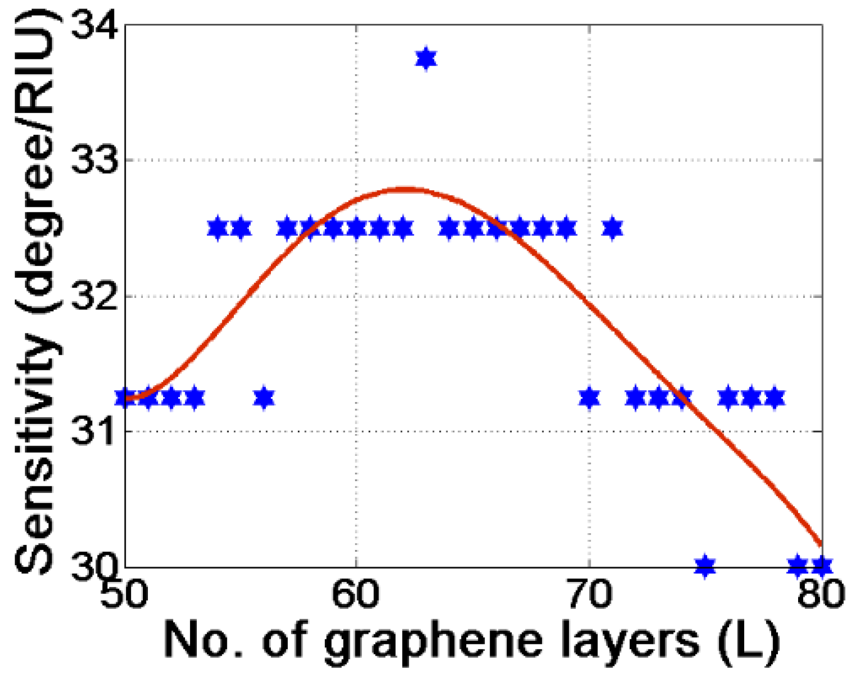
Figure 11 shows the sensitivity variation for the gas sensing probe with Au 50 nm and varying no. of graphene layers. The silicon layer is absent in this particular case. Maximum sensitivity is calculated to be only 34.40 degree/RIU, which is again very low compared to the probe with a silicon layer. This again confirms the role of silicon in sensitivity enhancement.
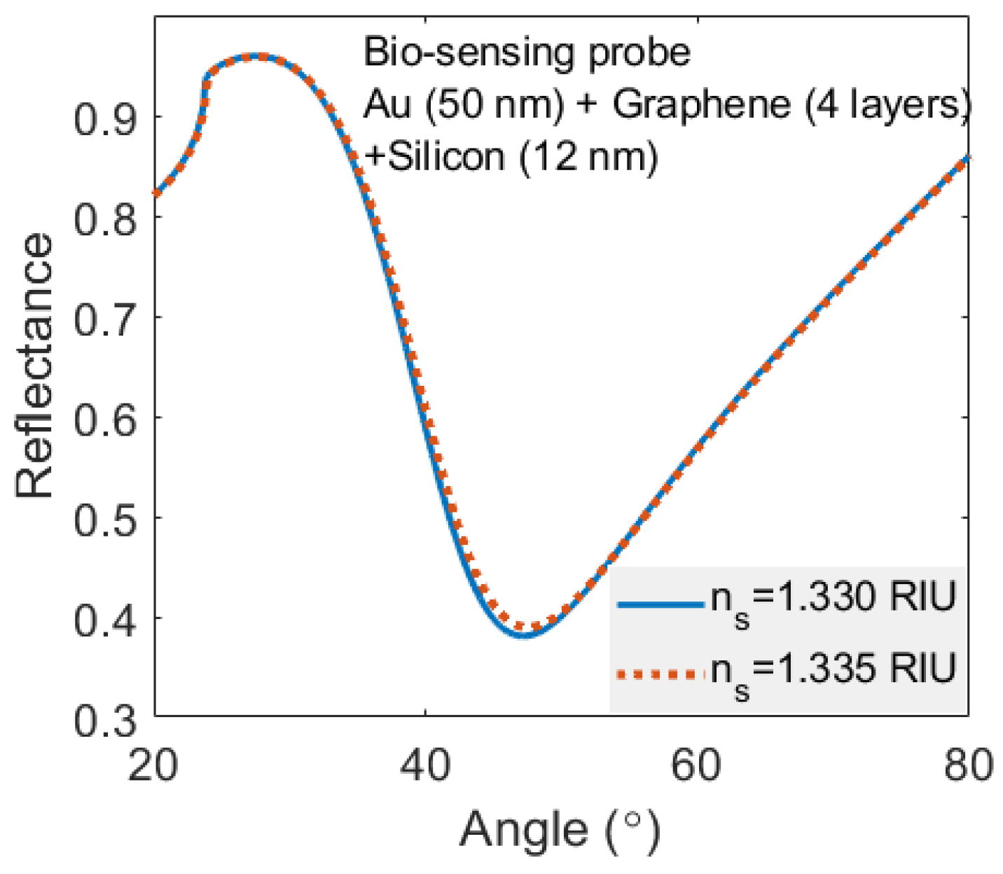
The SPR curve for an optimized bio-probe with Au (50 nm)/graphene (four layers)/silicon (12 nm) is shown in
Figure 12.
4. Conclusions
In summary, a novel SPR-based sensor design, having potential for the detection of both gas and bio samples, has been proposed and characterized. The sensor has a field enhancing silicon layer and an adsorbing graphene layer. The sensitivities for detection of gas and bio samples are calculated to be 53.75 degree/RIU and 72.60 degree/RIU, respectively at an interrogation wavelength of 632 nm. The optimized sensing probe’s design parameters for gas and bio-sensing are, respectively, Au (50 nm)/graphene (13 layers)/silicon (11 nm) and Au (50 nm)/graphene (4 layers)/silicon (12 nm). Alongside this, DA analysis has also been performed.


