Simulation Study on the Effect of Doping Concentrations on the Photodetection Properties of Mg2Si/Si Heterojunction Photodetector


Abstract
:1. Introduction
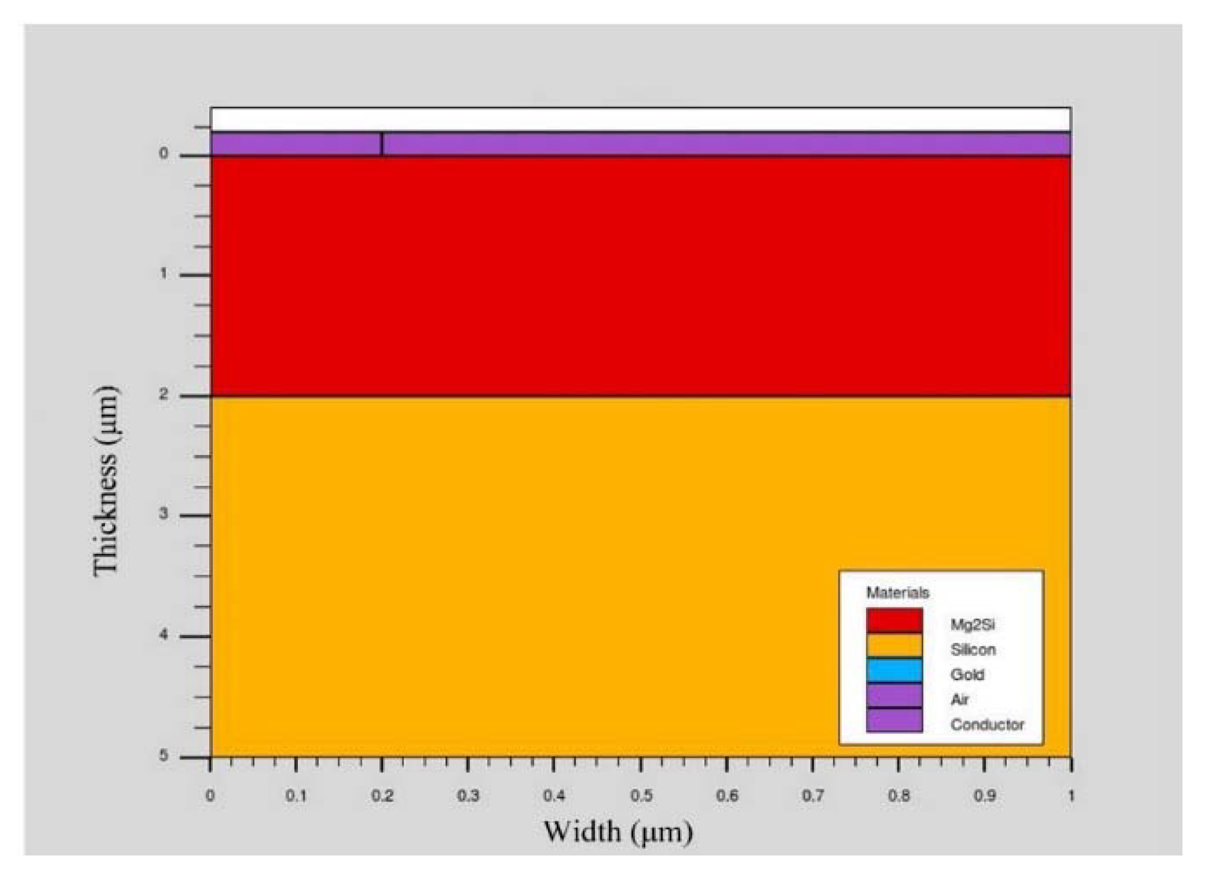
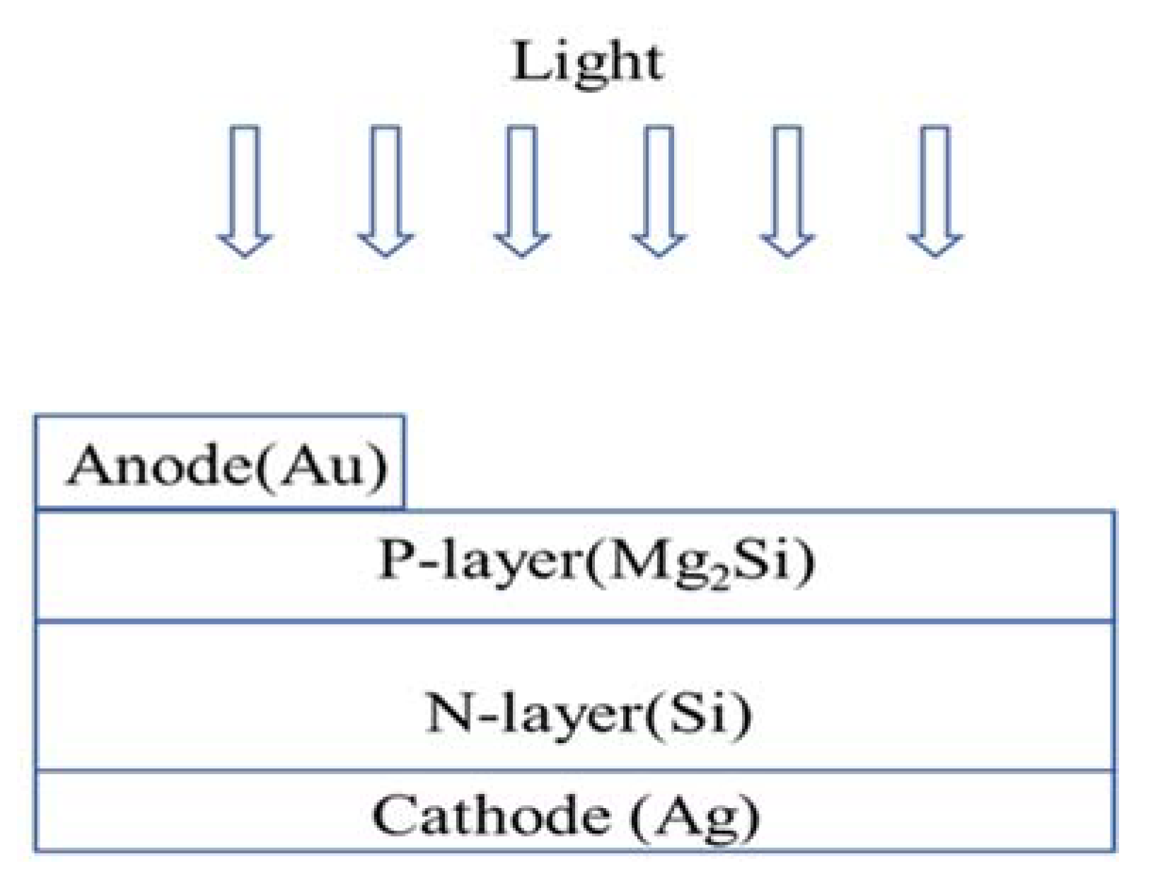
2. Simulation Method and Device Structure
3. Results and Discussion
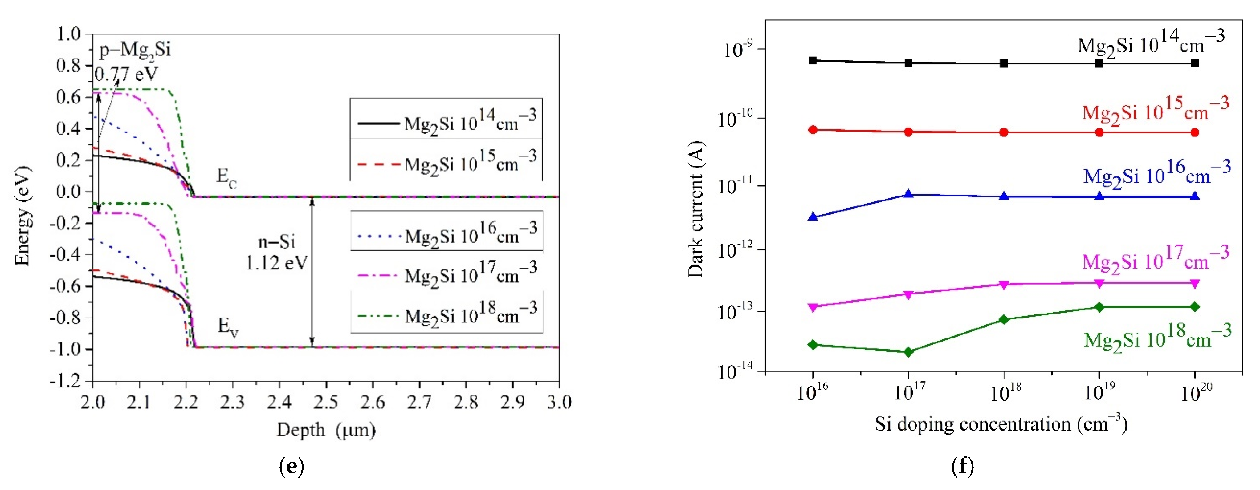
3.1. Energy Band
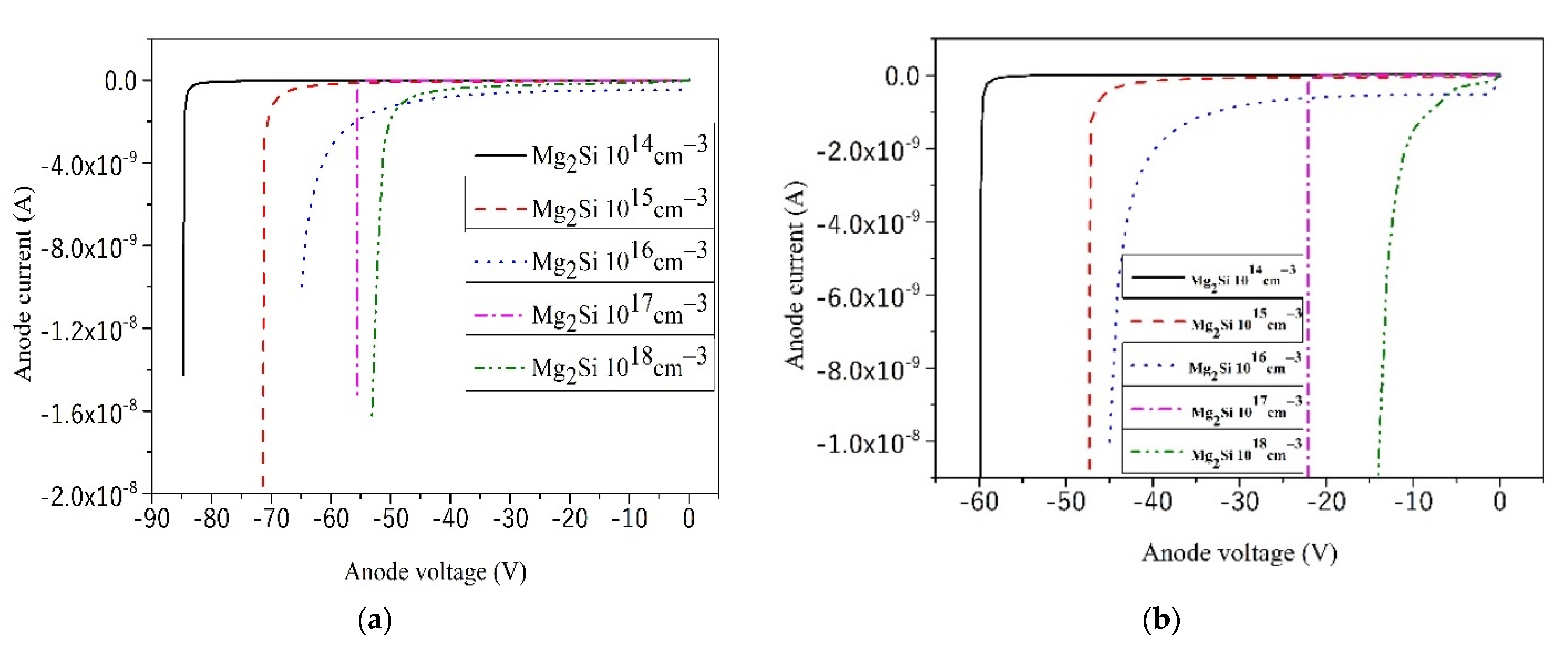
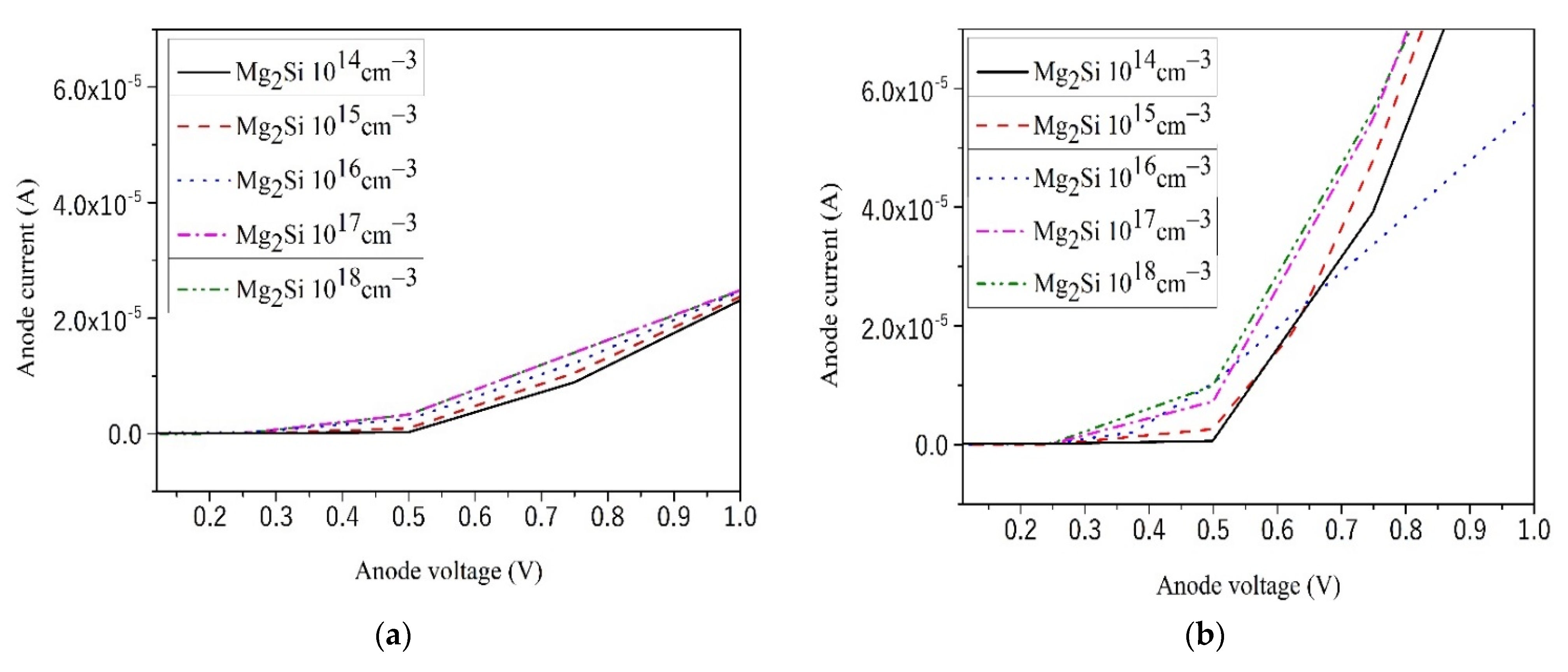
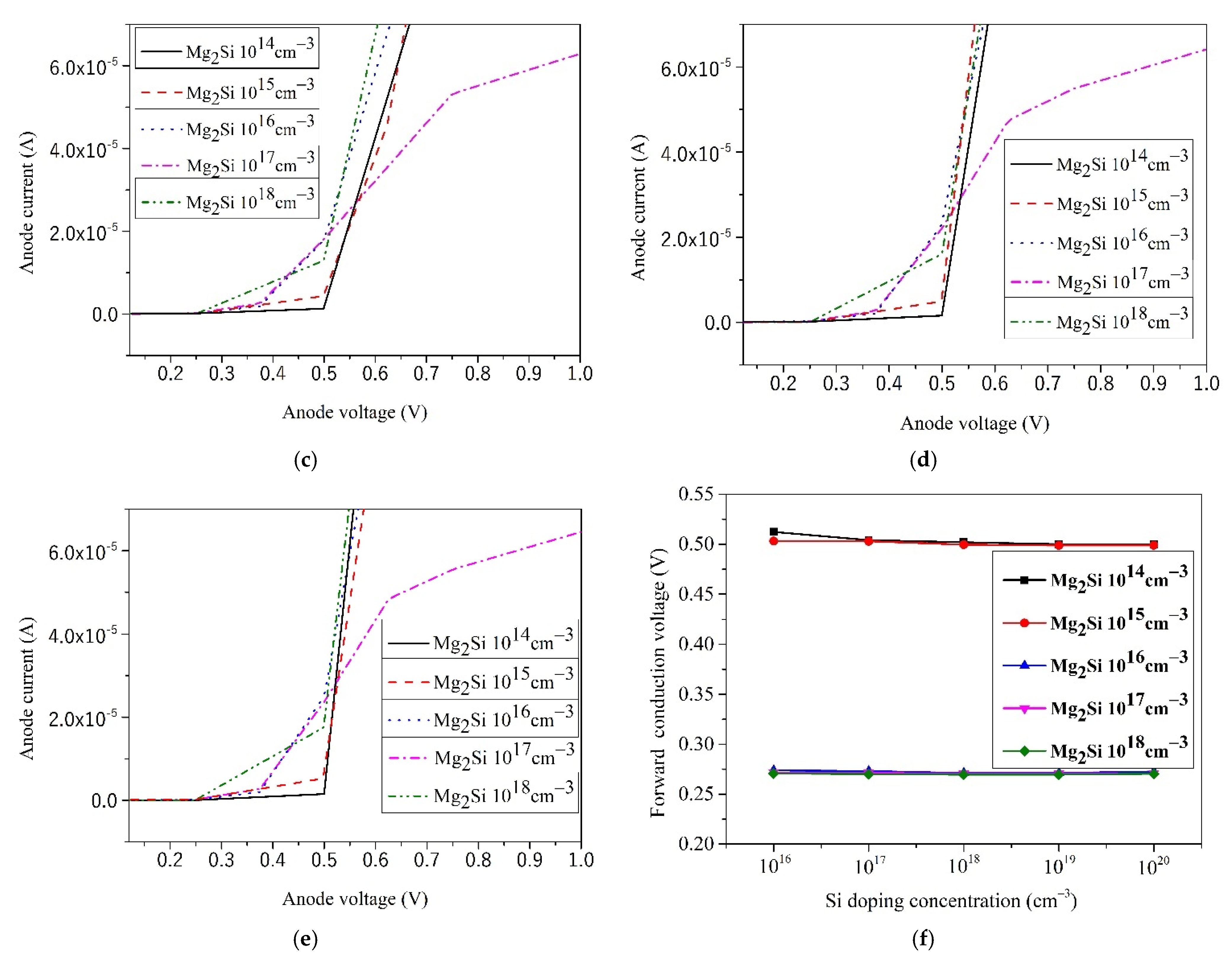
3.2. Current–Volage (I–V) Curves
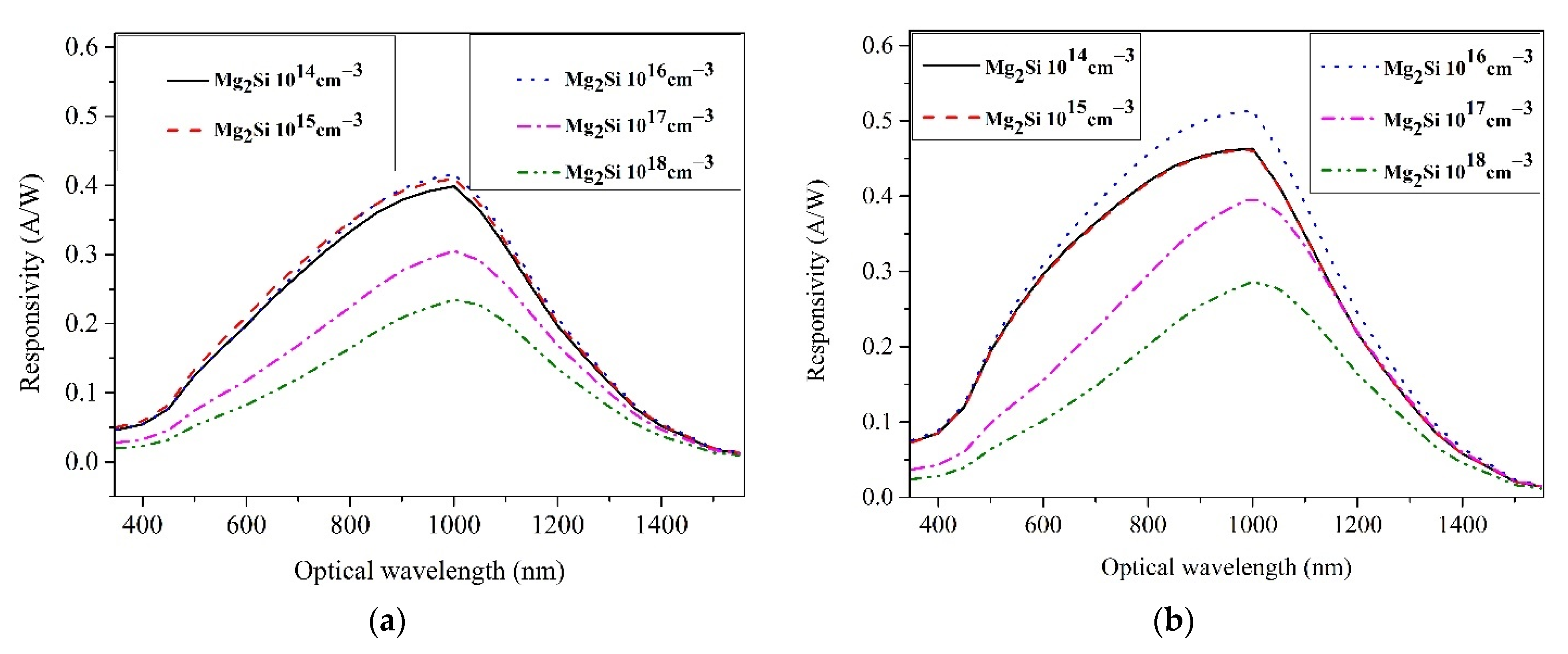
3.3. Responsivity
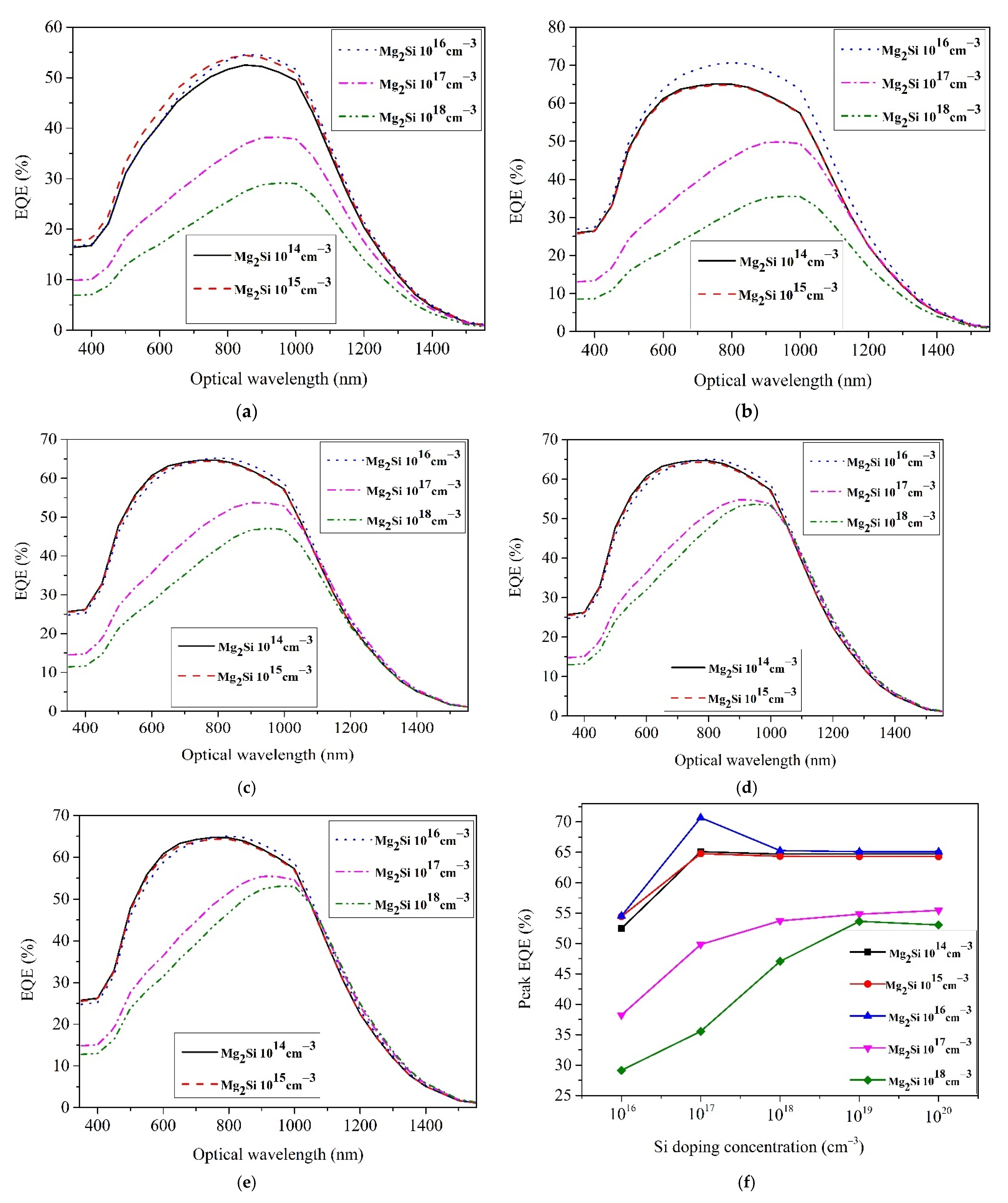
3.4. External Quantum Efficiency (EQE)
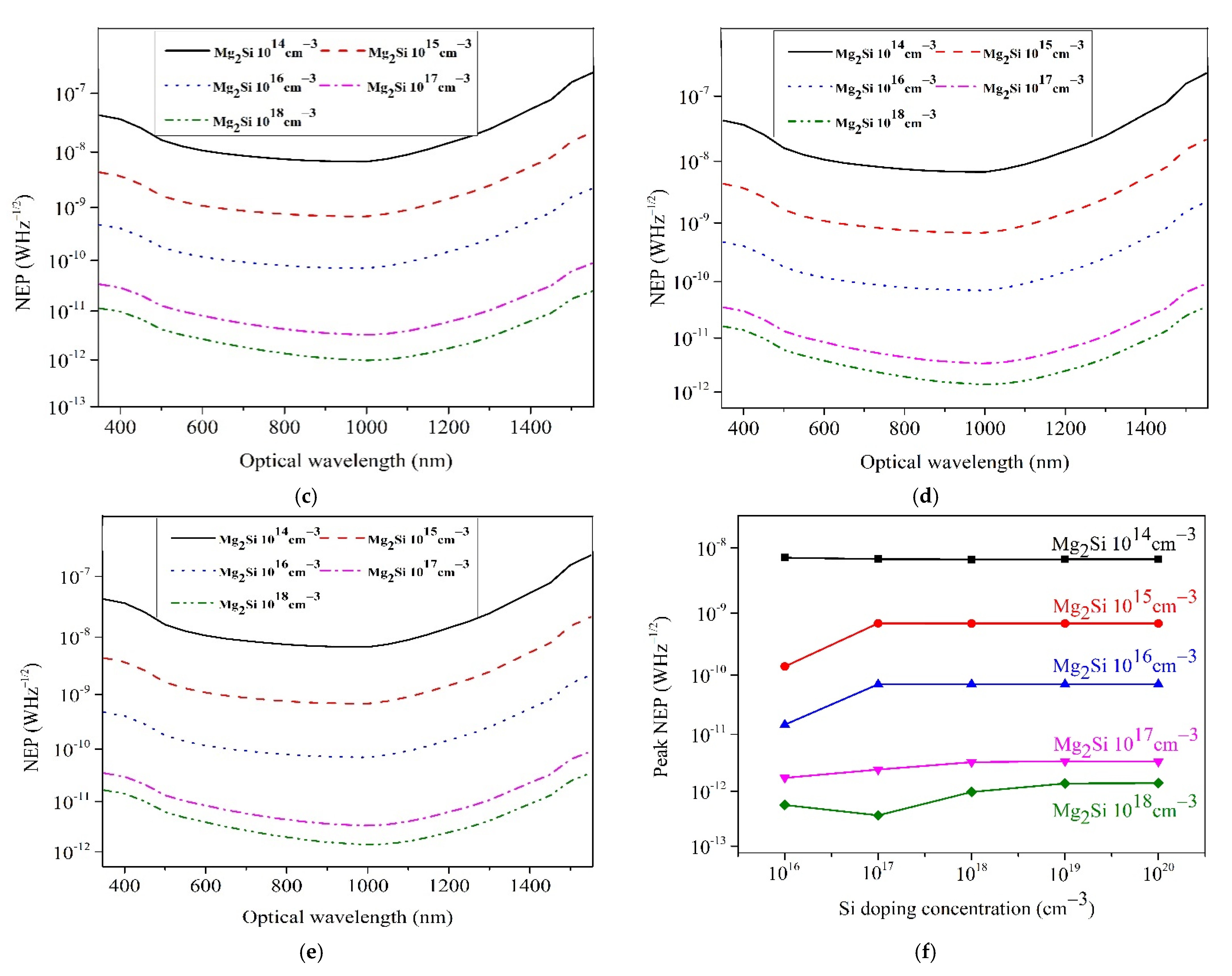
3.5. Noise Equivalent Power (NEP)
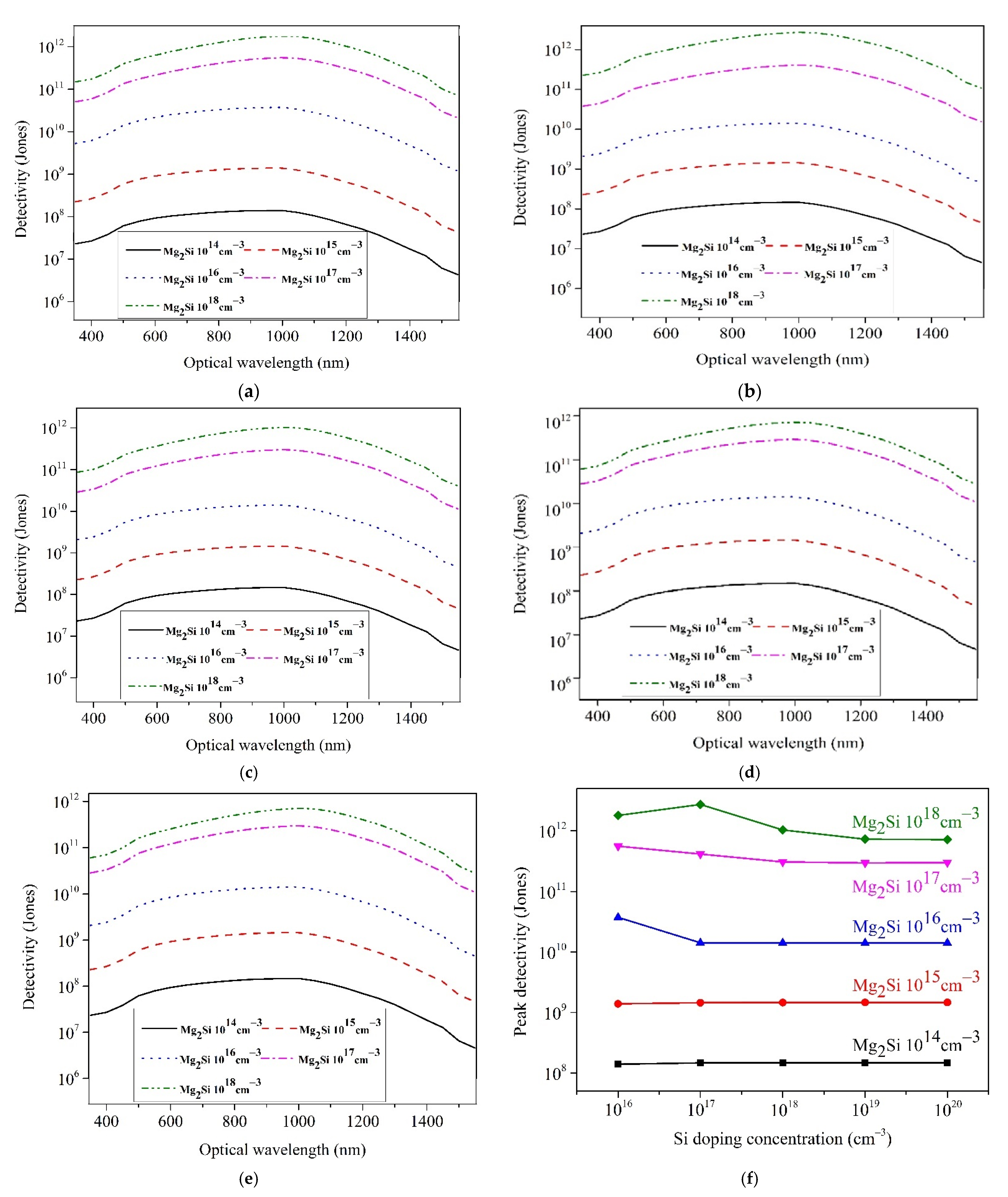
3.6. Detectivity
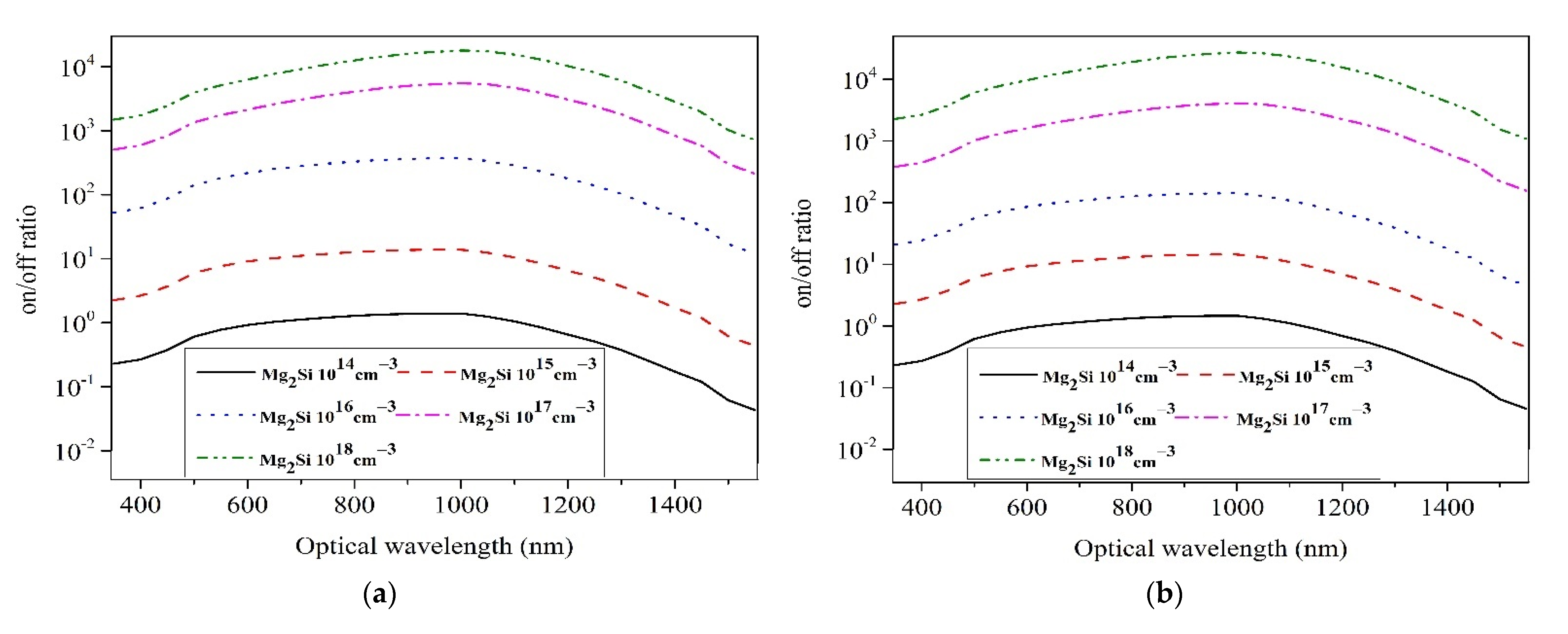
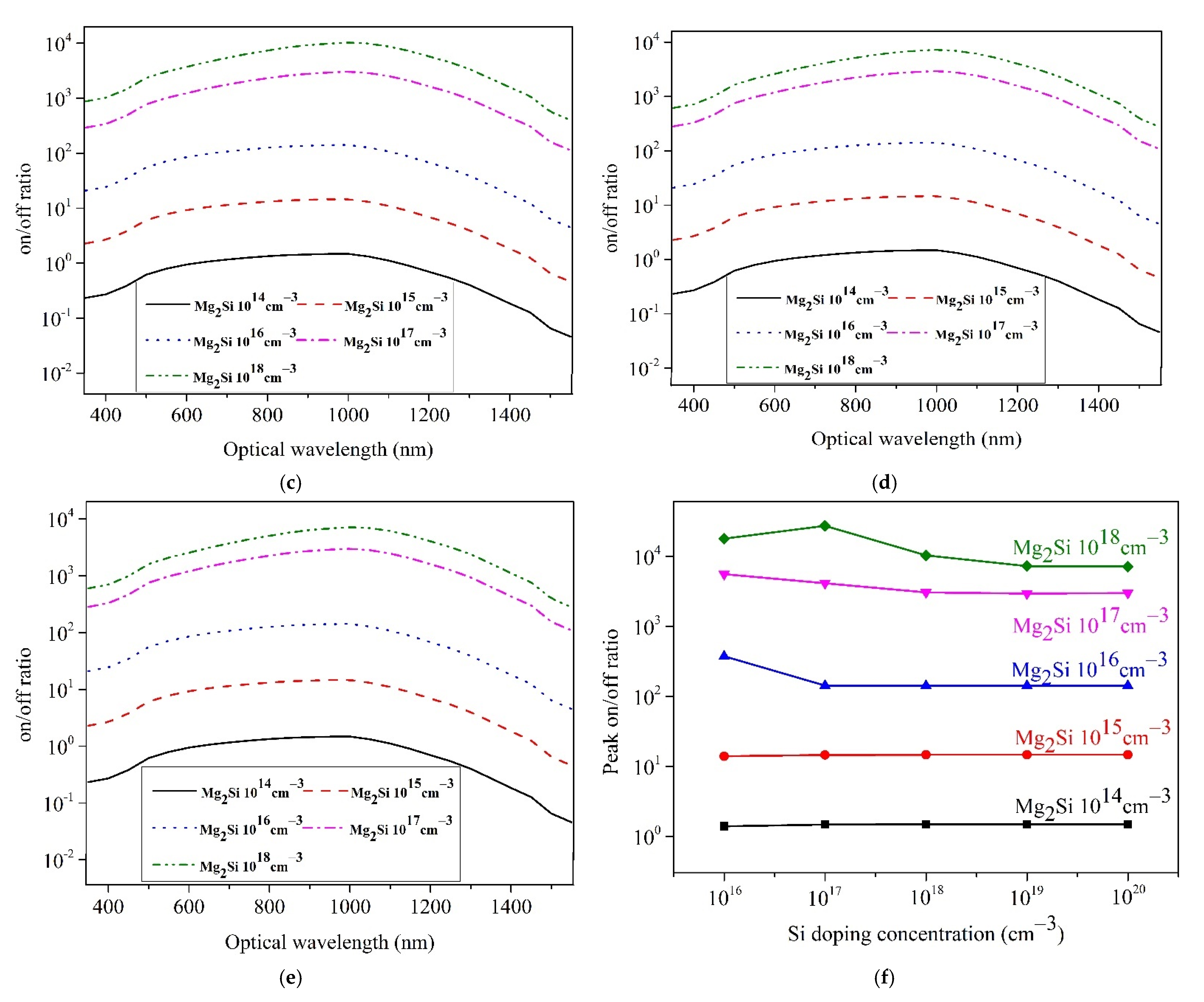
3.7. On/Off Ratio
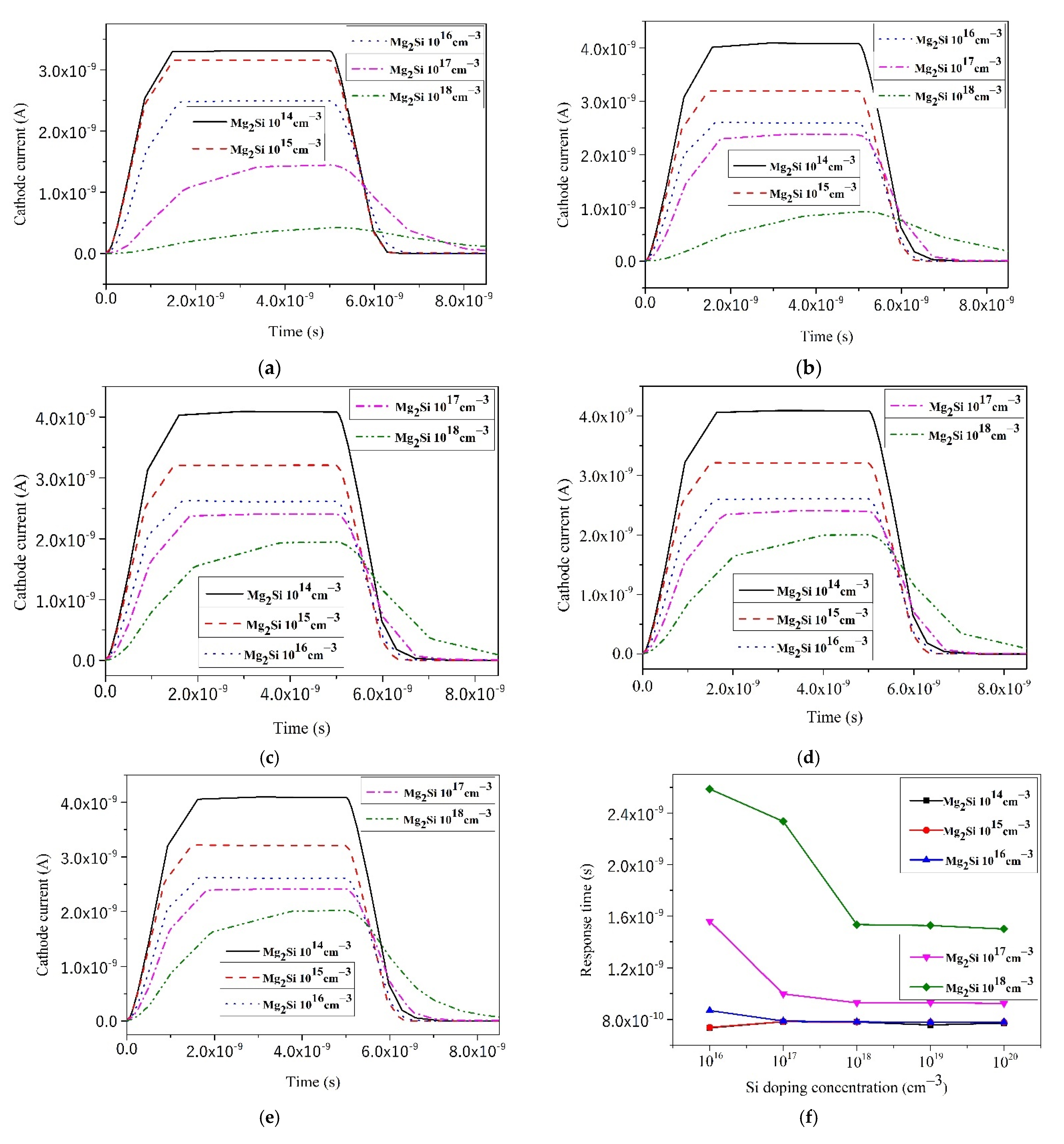
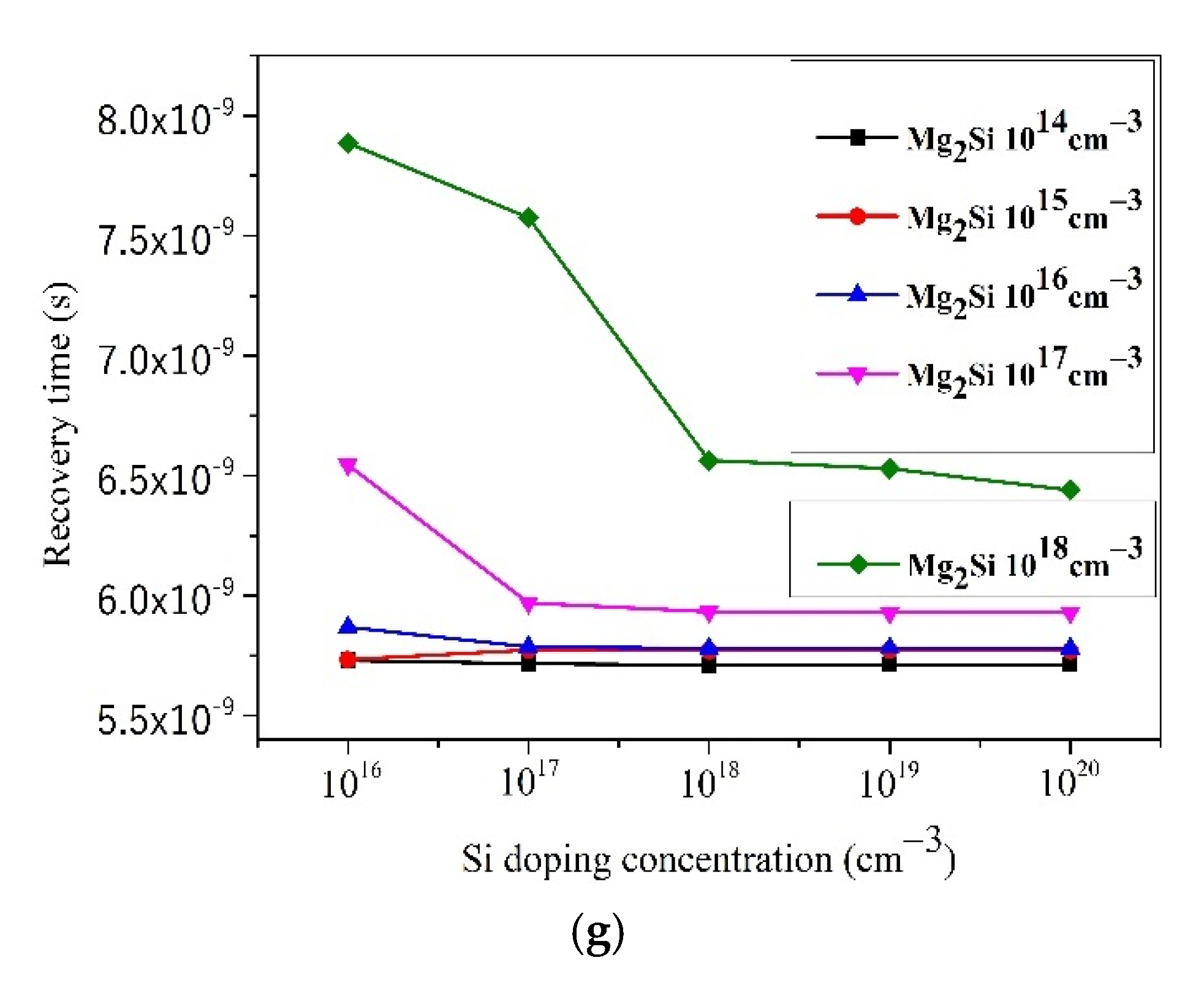
3.8. Response Time and Recovery Time
4. Conclusions
Author Contributions
Funding
Institutional Review Board Statement
Informed Consent Statement
Data Availability Statement
Conflicts of Interest
References
- El-Amir, A.; Ohsawa, T.; Nabatame, T.; Ohi, A.; Wada, Y.; Nakamura, M.; Fu, X.; Shimamura, K.; Ohashi, N. Ecofriendly Mg2Si-based photodiode for short-wavelength IR sensing. Mater. Sci. Semicon. Proc. 2019, 91, 222–229. [Google Scholar] [CrossRef]
- Kato, T.; Sago, Y.; Fujiwara, H. Optoelectronic properties of Mg2Si semiconducting layers with high absorption coefficients. J. Appl. Phys. 2011, 110, 063723. [Google Scholar] [CrossRef]
- Tamura, D.; Nagai, R.; Sugimoto, K.; Udono, H.; Kikuma, I.; Tajima, H.; Ohsugi, I.J. Melt growth and characterization of Mg2Si bulk crystals. Thin Solid Film. 2007, 515, 8272–8276. [Google Scholar] [CrossRef]
- Udono, H.; Yamanaka, Y.; Uchikoshi, M.; Isshiki, M. Infrared photoresponse from pn-junction Mg2Si diodes fabricated by thermal diffusion. J. Phys. Chem. Solids 2013, 74, 311–314. [Google Scholar] [CrossRef]
- Udono, H.; Tajima, H.; Uchikoshi, M.; Itakura, M. Crystal growth and characterization of Mg2Si for IR–detectors and thermoelectric applications. Jpn. J. Appl. Phys. 2015, 54, 07JB06. [Google Scholar] [CrossRef]
- Yang, M.Y.; Cohen, M.L. Electronic structure and pptical properties of Mg2Si, Mg2Ge, and Mg2Sn. Phys. Rev. 1969, 178, 1358–1364. [Google Scholar] [CrossRef]
- Madan, J.; Dassi, M.; Pandey, R.; Chaujar, R.; Sharma, R. Numerical analysis of Mg2Si/Si heterojunction DG-TFET for low power/high performance applications: Impact of non-idealities. Superlattice Microst. 2020, 139, 106397. [Google Scholar] [CrossRef]
- Pathania, A.; Madan, J.; Pandey, R.; Sharma, R. Effect of structural and temperature variations on perovskite/Mg2Si based monolithic tandem solar cell structure. Appl. Phys. A 2020, 126, 580. [Google Scholar] [CrossRef]
- Gao, Y.; Liu, H.W.; Lin, Y.; Shao, G. Computational design of high efficiency FeSi2 thin film solar cells. Thin Solid Film. 2011, 24, 8490–8495. [Google Scholar] [CrossRef]
- Deng, Q.; Wang, Z.; Wang, S.; Shao, G. Simulation of planar Si/Mg2Si/Si p-i-n heterojunction solar cells for high efficiency. Sol. Energy 2017, 158, 654–662. [Google Scholar] [CrossRef]
- Shevlyagin, A.; Chernev, I.; Galkin, N.; Gerasimenko, A.; Gutakovskii, A.; Hoshida, H.; Terai, Y.; Nishikawa, N.; Ohdaira, K. Probing the Mg2Si/Si(111) heterojunction for photovoltaic applications. Sol. Energy 2020, 211, 383–395. [Google Scholar] [CrossRef]
- Neamen, D.A. Semiconductor Physics and Devices: Basic Principles, 3th ed.; McGraw-Hill: New York, NY, USA, 2003; pp. 171–226. [Google Scholar]
- Ahn, D.; Hong, C.Y.; Liu, J.F.; Giziewicz, W.; Beals, M.; Kimerling, L.C.; Michel, J.; Chen, J.; Kärtner, F.X. High performance, waveguide integrated Ge photodetectors. Opt. Express 2007, 15, 3916–3921. [Google Scholar] [CrossRef]
- Chen, Y.J.; Li, M.H.; Liu, J.Y.; Chong, C.W.; Huang, J.C.A.; Chen, P. Double-side operable perovskite photodetector using Cu/Cu2O as a hole transport layer. Opt. Express 2019, 27, 24900–24913. [Google Scholar] [CrossRef]
- Zhu, M.; Li, X.M.; Guo, Y.B.; Li, X.; Sun, P.Z.; Zang, X.B.; Wang, K.L.; Zhong, M.L.; Wu, D.H.; Zhu, H.W. Vertical junction photodetectors based on reduced graphene oxide/silicon Schottky diodes. Nanoscale 2014, 6, 4909–4914. [Google Scholar] [CrossRef]
- Li, X.M.; Zhu, M.; Du, M.D.; Lv, Z.; Zhang, L.; Li, Y.C.; Yang, Y.; Yang, T.T.; Li, X.; Wang, K.L.; et al. High Detectivity Graphene-Silicon Heterojunction Photodetector. Small 2016, 12, 595–601. [Google Scholar] [CrossRef] [PubMed]
- Sharma, S.; Sumathi, A.; Periasamy, C. Photodetection Properties of ZnO/Si Heterojunction Diode: A Simulation Study. IETE Tech. Rev. 2017, 34, 83–90. [Google Scholar] [CrossRef]
- Zhu, M.; Zhang, L.; Li, X.M.; He, Y.J.; Li, X.; Guo, F.M.; Zang, X.B.; Wang, K.L.; Xie, D.; Li, X.H.; et al. TiO2 enhanced ultraviolet detection based on a graphene/Si Schottky diode. J. Mater. Chem. A 2015, 3, 8133–8138. [Google Scholar] [CrossRef] [Green Version]
- Zhang, L.F.; Wan, P.; Xu, T.; Kan, C.X.; Jiang, M.M. Flexible ultraviolet photodetector based on single ZnO microwire/polyaniline heterojunctions. Opt. Express 2021, 29, 19202–19213. [Google Scholar] [CrossRef]
- Chen, M.Z.; Ma, J.G.; Li, P.; Xu, H.Y.; Liu, Y.C. Zero-biased deep ultraviolet photodetectors based on graphene/cleaved (100) Ga2O3 heterojunction. Opt. Express 2019, 27, 8717–8726. [Google Scholar] [CrossRef] [PubMed]
- Li, X.; Sun, T.; Zhou, K.; Hong, X.; Tang, X.; Wei, D.; Feng, W.; Shen, J.; Wei, D. Broadband InSb/Si heterojunction photodetector with graphene transparent electrode. Nanotechnology 2020, 31, 315204. [Google Scholar] [CrossRef]
- Shao, J.; Yao, J.; Wang, Y.; Zhao, Z.; Yang, G. Ultra-broadband and high response of the Bi2Te3/Si Heterojunction and its application as a photodetector at room temperature in harsh working environments. Nanoscale 2015, 7, 12535–12541. [Google Scholar]
- Wetzel, C.; Takeuchi, T.; Amano, H.; Akasaki, I. Piezoelectric Franz-Keldysh effect in strained GaInN/GaN heterostructures. J. Appl. Phys. 1999, 85, 3786–3791. [Google Scholar] [CrossRef] [Green Version]
- Sato, T.; Kumazaki, Y.; Kida, H.; Watanabe, A.; Yatabe, Z.; Matsuda, S. Large photocurrents in GaN porous structures with a redshift of the photoabsorption edge. Semicond. Sci. Technol. 2016, 31, 014012. [Google Scholar] [CrossRef] [Green Version]
- Takuya, M.; Xilun, C.; Masahiro, H.; Jun, S.; Tsunenobu, K. Phonon-assisted optical absorption due to Franz-Keldysh effect in 4H-SiC p-n junction diode under high reverse bias voltage. Appl. Phys. Express 2018, 11, 091302. [Google Scholar]
- Hao, L.; Wang, Z.; Xu, H.; Yan, K.; Dong, S.; Liu, H.; Du, Y.; Wu, Y.; Liu, Y.; Dong, M. 2D SnSe/Si heterojunction for self-driven broadband photodetectors. 2D Mater. 2019, 6, 034004. [Google Scholar] [CrossRef]
- Wu, E.; Wu, D.; Jia, C.; Wang, Y.; Yuan, H.; Zeng, L.; Xu, T.; Shi, Z.; Tian, Y.; Li, X. In situ fabrication of 2D WS2/Si type-II heterojunction for self-powered broadband photodetector with response up to mid-infrared. ACS Photonics 2019, 6, 565–572. [Google Scholar] [CrossRef] [Green Version]
- Bansal, S.; Das, A.; Jain, P.; Prakash, K.; Sharma, K.; Kumar, N.; Sardana, N.; Gupta, N.; Kumar, S.; Singh, A.K. Enhanced optoelectronic properties of bilayer Graphene/HgCdTe–based single– and dual–junction photodetectors in long infrared regime. IEEE Trans. Nanotechnol. 2019, 18, 781–789. [Google Scholar] [CrossRef]
- Yang, B.; Zhao, Y.Y.; Chen, J. High sensitivity graphene-Al2O3 passivated InGaAs near-infrared photodetector. Nanotechnology 2021, 32, 455503. [Google Scholar] [CrossRef]
- Wu, D.; Guo, J.W.; Wang, C.Q.; Ren, X.Y.; Chen, Y.S.; Lin, P.; Zeng, L.H.; Shi, Z.F.; Li, X.J.; Shan, C.X.; et al. Ultrabroadband and High-Detectivity Photodetector Based on WS2/Ge Heterojunction through Defect Engineering and Interface Passivation. ACS Nano 2021, 15, 10119–10129. [Google Scholar] [CrossRef] [PubMed]
- Dang, Z.Y.; Wang, W.H.; Chen, J.Y.; Walker, E.S.; Bank, S.R.; Akinwande, D.; Ni, Z.H.; Tao, L. Vis-NIR photodetector with microsecond response enabled by 2D bismuth/Si(111) heterojunction. 2D Mater. 2021, 8, 035002. [Google Scholar] [CrossRef]
- Mattia, S.; Matteo, S.; Federico, F.; Daniele, C.; Lorenzo, D.M.; Maurizio, B.; Maurizio, D.C.; Paola, C. Carbon nanotube film/silicon heterojunction photodetector for new cutting–edge technological devices. Appl. Sci. 2021, 11, 606. [Google Scholar]
- Tu, W.C.; Shih, Y.H.; Huang, J.H.; Chen, Y.C. Semi-transparent reduced graphene oxide photodetectors for ultra-low power operation. Opt. Express 2021, 29, 14208–14217. [Google Scholar] [CrossRef] [PubMed]
- Xin, Y.; Jiang, J.C.; Lu, Y.F.; Liang, H.W.; Zeng, Y.J.; Ye, Z.Z. Self-Powered Broad Spectral Photodetector with Ultrahigh Responsivity and Fast Response Based on Sb2Se3/VO2 Heterojunction. Adv. Mater. Interfaces 2021, 8, 2100058. [Google Scholar] [CrossRef]
- Chandra, K.; Reddy, S.; Sahatiya, P.; Sauceda, I.S.; Cortázar, O.; Bon, R.R. One-step fabrication of 1D p-NiO nanowire/n-Si heterojunction: Development of self-powered ultraviolet photodetector. Appl. Surf. Sci. 2020, 513, 145804. [Google Scholar] [CrossRef]
- Tong, X.W.; Wang, J.J.; Li, J.X.; Hu, X.F.; Wu, D.; Luo, L.B. Enhancing the device performance of SiNP array/PtTe2 heterojunction Photodetector by the light trapping effect. Sens. Actuators A–Phys. 2021, 322, 112625. [Google Scholar] [CrossRef]


| Parameters and Units | Mg2Si [7,8] | Si [9] |
|---|---|---|
| Bandgap (eV) | 0.77 | 1.12 |
| Affinity (eV) | 4.37 | 4.05 |
| Permittivity | 20 | 11.9 |
| Effective conduction band density (cm−3) | 7.8 × 10¹⁸ | 2.8 × 10¹⁹ |
| Effective valence band density (cm−3) | 2.06 × 10¹⁹ | 1.04 × 10¹⁹ |
| Electron mobility (cm2/Vs) | 550 | 1350 |
| Hole mobility (cm2/Vs) | 70 | 500 |
| Electron auger coefficient (cm6/s) | 9 × 10⁻²⁹ | 2.8 × 10⁻³¹ |
| Hole auger coefficient (cm6/s) | 9 × 10⁻²⁹ | 9.9 × 10⁻³² |
| SRH recombination life time, e, h (s) | 1 × 10⁻⁶ | 1 × 10⁻⁷ |
| Device | Responsivity (A/W) | EQE (%) | NEP (WHz–1/2) | Detectivity (Jones) | On-off Ratio | Spectral Range (nm) | References |
|---|---|---|---|---|---|---|---|
| Mg2Si/Si | 0.51 | 70.68 | 7.07 × 10⁻¹¹ | 1.4 × 10¹⁰ | 1.4 × 10² | 400–1500 | This work |
| Gr/Si | 0.73 | 7.5 × 10⁻¹⁴ | 4.2 × 10¹² | 300–1100 | [16] | ||
| ZnO/Si | 0.36 | 93 | 10−11 | 7.2 × 10¹⁰ | 200–1000 | [17] | |
| InSb/Si | 0.312 | 25 | 1.15 × 10⁻¹² | 6.7 × 10¹⁰ | 2.9 × 10³ | 635–2700 | [21] |
| Bi2Te3/Si | 1 | 120 | 2.5 × 10¹¹ | [22] | |||
| SnSe/Si | 0.566 | 4.4 × 10¹² | 4.9 × 10⁵ | 300–1100 | [25] | ||
| WS2/Si | 0.224 | 1.5 × 10¹² | 106 | 200–3043 | [26] | ||
| Gr/HgCdTe Gr/Al2O3/In- GaAs | 7.33 0.52 | 85.8 | 4.72 × 10⁻²⁰ | 4.4 × 10¹⁰ | 2000–12,000 | [27,28] |
Publisher’s Note: MDPI stays neutral with regard to jurisdictional claims in published maps and institutional affiliations. |
© 2021 by the authors. Licensee MDPI, Basel, Switzerland. This article is an open access article distributed under the terms and conditions of the Creative Commons Attribution (CC BY) license (https://creativecommons.org/licenses/by/4.0/).
Share and Cite
Yu, H.; Gao, C.; Zou, J.; Yang, W.; Xie, Q. Simulation Study on the Effect of Doping Concentrations on the Photodetection Properties of Mg2Si/Si Heterojunction Photodetector. Photonics 2021, 8, 509. https://doi.org/10.3390/photonics8110509
Yu H, Gao C, Zou J, Yang W, Xie Q. Simulation Study on the Effect of Doping Concentrations on the Photodetection Properties of Mg2Si/Si Heterojunction Photodetector. Photonics. 2021; 8(11):509. https://doi.org/10.3390/photonics8110509
Chicago/Turabian StyleYu, Hong, Chenggui Gao, Jiang Zou, Wensheng Yang, and Quan Xie. 2021. "Simulation Study on the Effect of Doping Concentrations on the Photodetection Properties of Mg2Si/Si Heterojunction Photodetector" Photonics 8, no. 11: 509. https://doi.org/10.3390/photonics8110509
APA StyleYu, H., Gao, C., Zou, J., Yang, W., & Xie, Q. (2021). Simulation Study on the Effect of Doping Concentrations on the Photodetection Properties of Mg2Si/Si Heterojunction Photodetector. Photonics, 8(11), 509. https://doi.org/10.3390/photonics8110509