Review

III-Nitride Light-Emitting Devices

1
Department of Electrical and Electronic Engineering, Bangladesh University of Engineering and Technology, Dhaka 1000, Bangladesh
2
Department of Electrical Engineering & Computer Science, The University of Tennessee, Knoxville, TN 37996, USA
*
Author to whom correspondence should be addressed.
Photonics 2021, 8(10), 430; https://doi.org/10.3390/photonics8100430
Submission received: 28 August 2021 / Revised: 3 October 2021 / Accepted: 4 October 2021 / Published: 7 October 2021
(This article belongs to the Special Issue Emerging Photonic Devices, Circuits and Systems)

Abstract

:
III-nitride light-emitting devices have been subjects of intense research for the last several decades owing to the versatility of their applications for fundamental research, as well as their widespread commercial utilization. Nitride light-emitters in the form of light-emitting diodes (LEDs) and lasers have made remarkable progress in recent years, especially in the form of blue LEDs and lasers. However, to further extend the scope of these devices, both below and above the blue emission region of the electromagnetic spectrum, and also to expand their range of practical applications, a number of issues and challenges related to the growth of materials, device design, and fabrication need to be overcome. This review provides a detailed overview of nitride-based LEDs and lasers, starting from their early days of development to the present state-of-the-art light-emitting devices. Besides delineating the scientific and engineering milestones achieved in the path towards the development of the highly matured blue LEDs and lasers, this review provides a sketch of the prevailing challenges associated with the development of long-wavelength, as well as ultraviolet nitride LEDs and lasers. In addition to these, recent progress and future challenges related to the development of next-generation nitride emitters, which include exciton-polariton lasers, spin-LEDs and lasers, and nanostructured emitters based on nanowires and quantum dots, have also been elucidated in this review. The review concludes by touching on the more recent topic of hexagonal boron nitride-based light-emitting devices, which have already shown significant promise as deep ultraviolet and single-photon emitters.

1. Introduction

III-nitride materials are the materials of choice for a wide range of applications and scientific explorations spanning across the fields of power electronics, optoelectronics, photonics, logic circuits, spintronics, high-temperature electronics, and communication technology. Within this variegated array of fields, optoelectronics is one of the most promising ones owing to the suitability of III-nitride material systems as the near-perfect solution to numerous challenges [1,2]. The direct bandgap nature of III-nitrides, coupled with their tunable emission characteristics, spanning from deep ultraviolet (DUV) to the near-infrared (NIR) region of the electromagnetic (EM) spectrum, makes this material system uniquely suitable for a wide range of photonic solutions. The exotic electronic properties of III-nitrides, such as the high exciton-binding energy, large breakdown fields, and high-temperature stability, make these material systems all the more suitable for room temperature operation under electrical injection, thereby offering the prospect of controlling light output and absorption characteristics via electronic means, based on optoelectronic devices, such as light-emitting diodes (LEDs), lasers, photodetectors, and optoelectronic integrated circuits (OEICs). The ability to grow high-quality quantum-confined structures in the form of quantum wells (QWs), wires, and dots has also facilitated the realization of III-nitride-based optoelectronic devices with unusual properties and high-performance characteristics. In spite of the high defect density of this material system and challenges associated with p-doping, remarkable advancements made in materials growth and device fabrication techniques have greatly paved the way for the successful realization of numerous III-nitride optoelectronic devices.
The most commonly employed III-nitride, wurtzite GaN, is a direct bandgap semiconductor with a bandgap of 3.4 eV. The zinc-blend variant of GaN is also a direct bandgap semiconductor, albeit with a much smaller bandgap of 1.49 eV. Wurtzite-InN and wurtzite-AlN are two other III-nitride binary compounds with bandgaps of 0.7 eV and 6 eV respectively [3]. As the band-to-band optical transition of these compounds corresponds to DUV and NIR wavelengths, by varying the indium and/or aluminum mole-fraction of InAlGaN alloys, the emission wavelength of III-nitrides can be conveniently tuned over the DUV-visible-NIR region of the EM spectrum (shown in Figure 1). Consequently, even though III-nitride compounds are popularly known for the commercialization of blue LED-based solid-state lighting (SSL) systems, nitride-based light-emitting devices hold significant promise for a wide range of other applications, such as display technologies, visible light communications, sensing, environmental monitoring, quantum information processing, optical storage, and so on (selected applications of III-nitride emitters are shown in Figure 1b). Over the last three decades, research and development of nitride-based LEDs and lasers has progressed at an incredible pace. In fact, the present-day maturity of materials growth, doping, and fabrication techniques related to III-nitrides can be largely credited to the remarkable progress being made with III-nitride LEDs and lasers. Even to date, new avenues of research relevant to these devices are being explored, not only to address existing challenges, but also to materialize disruptive technologies pertinent to numerous areas related to the ongoing fourth industrial revolution.
In this article, we present a comprehensive review of III-nitride-based emitters, namely LEDs and lasers, and discuss the future prospect of these devices based on the current research trends. This article is organized as follows. In Section 2, we first review the early research on III-nitride-based LEDs and their evolution from the first generation to state-of-the-art, high-performance nitride LEDs for solid-state lighting-related applications. Next, we discuss the research endeavors dedicated towards the development of nitride-based white LEDs, UV LEDs, and micro LEDs. The more recent research on the design and application of these devices for visible light communication is also discussed in this section. In Section 3, we present a detailed review of III-nitride-based lasers. In this section, discussions on the early development of nitride lasers are followed by an overview of the progress of blue and long-wavelength nitride lasers. Ongoing research and future prospects for nitride-based, edge-emitting, and vertical-cavity surface-emitting lasers are also discussed in this section. In Section 4, we provide an overview of next-generation nitride emitters, which include nitride-based exciton-polariton lasers, III-nitride spin-LEDs and lasers, and nanostructured nitride emitters. Finally, the review concludes with a brief discussion on the more recent topic of hexagonal boron nitride-based light-emitting devices, which have emerged as promising candidates for deep ultraviolet and single-photon emitters.

2. III-Nitride-Based LEDs

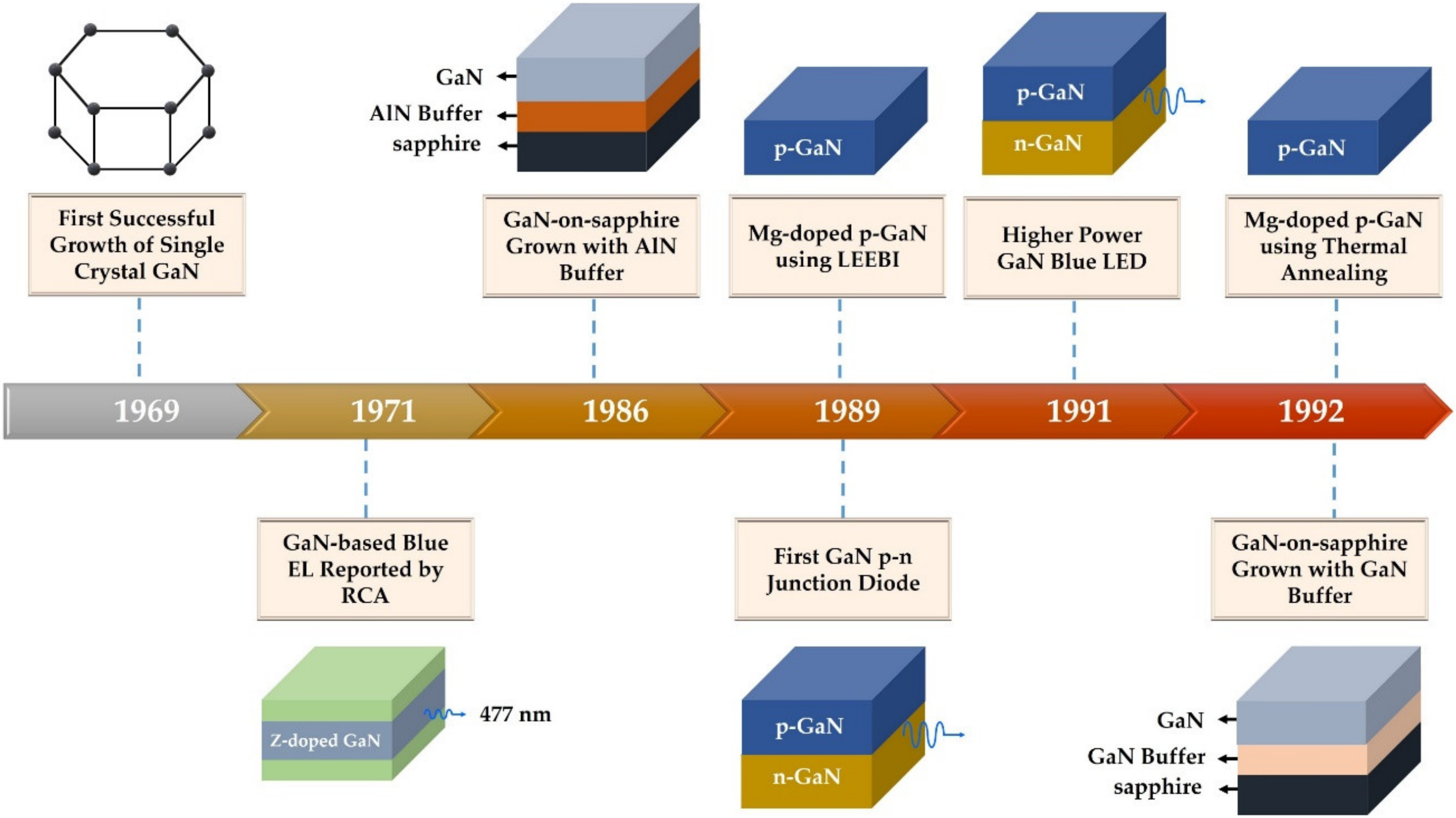
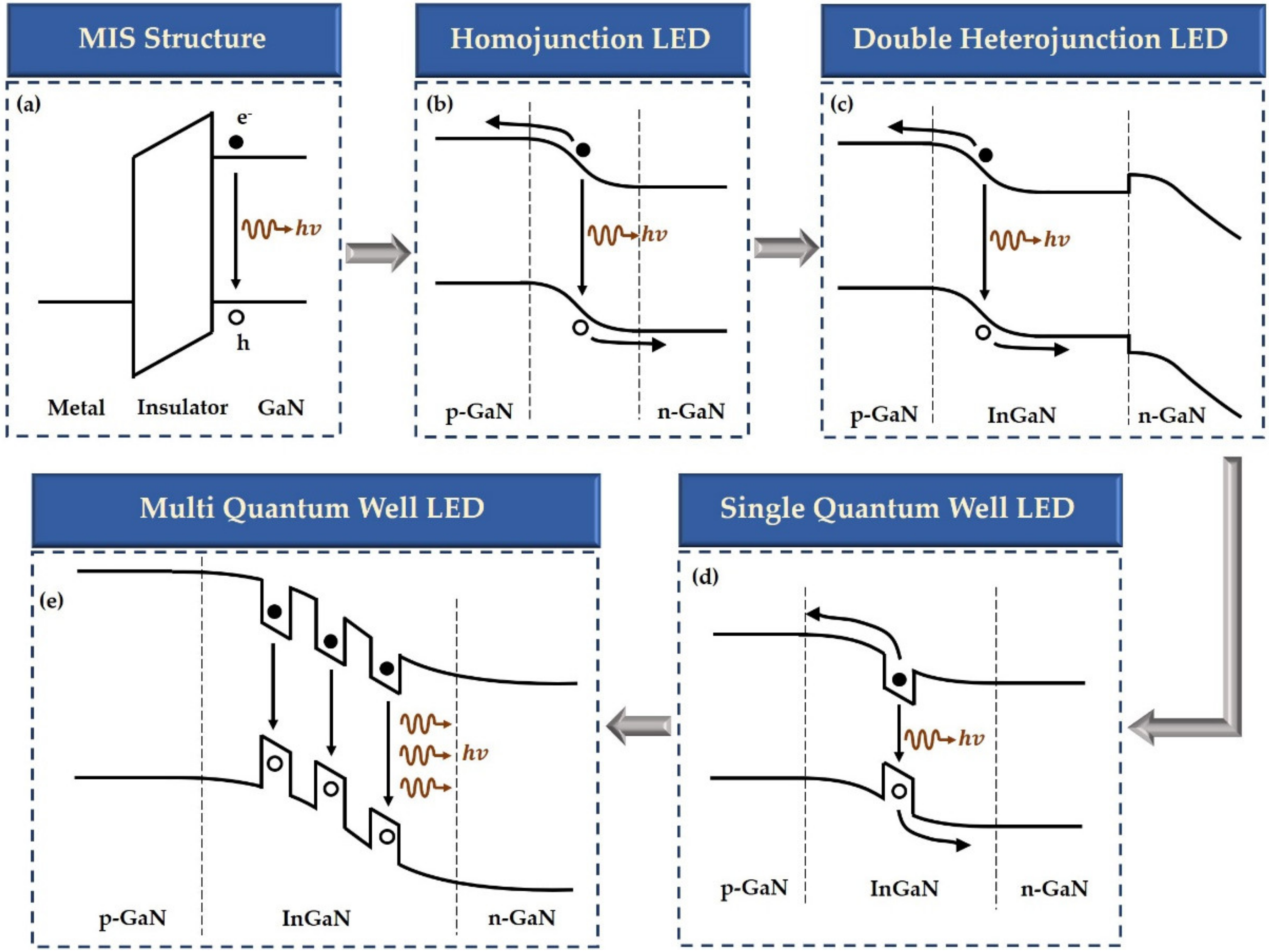
2.1. Early Development of Nitride LEDs

Advancements in the field of III-nitride optoelectronics can be largely attributed to the development of nitride-based LEDs. One of the main motivating factors behind the research on III-nitride LEDs was the experimental realization of a true-blue LED. Such an LED was commercially unavailable until the 1990s because of the non-compatibility of more commonly used direct bandgap semiconductors (such as GaAs, InP, GaP, etc.) at such short wavelength emissions. Back in the 1960s, several research groups attempted to grow nitride crystals with the aim of realizing a blue LED. The first successful growth of GaN single crystals was reported by Maruska and Tietjen in 1969 [4]. In their work, a single-crystal GaN was grown on a sapphire substrate using halide vapor phase epitaxy (HVPE), where GaCl and NH3 were used as the gaseous precursors. Based on such single-crystal material, blue electroluminescence from an electrically driven GaN device was first reported by RCA laboratories in 1971. The reported device had a metal-insulator-semiconductor (MIS) structure, and it was shown that, under electrical injection, a broad emission peak at 477 nm can be achieved in Zn-doped GaN when electrons recombine with holes generated by an avalanche breakdown at the grain boundaries [5,6]. The output of this device was limited to around 1–5 µW and the external quantum efficiency (EQE) was extremely low (~10−3). There were several other reports of MIS structure-based blue emissions from GaN [7,8,9,10]. In spite of these early successes, the development of a GaN-based blue LED faced significant challenges in terms of epitaxial growth because of the large number of defect states present in the material system. Moreover, attaining and controlling p-type conductivity appeared to be extremely challenging because of the self-compensation that resulted from the presence of a large number of nitrogen vacancies in GaN [11].
Significant breakthroughs towards the development of blue LEDs were made in the 1980s when high-quality GaN-on-sapphire was grown by metal-organic chemical vapor deposition (MOCVD), which employed AlN buffer layers on a sapphire substrate. This low-temperature-deposited buffer layer growth technique, pioneered by Akasaki et al. and Amano et al., enabled the growth of uniform crystalline-quality GaN films with good photoluminescence and electrical properties [12,13,14]. The same technique was employed by Nakamura et al. to attain high-quality thin films using a GaN-buffer layer instead of the AlN-buffer [15]. The room temperature Hall mobility of these films was 600 cm2/V-s, whereas for the AlN-buffer-based films, the mobility was in the 350–400 cm2/V-s range. Another significant milestone towards the development of GaN-based LEDs was achieved in the late 1980s, when Amano et al. reported the first successful p-doping of GaN with Mg-acceptors through the utilization of ex situ low-energy electron beam irradiation (LEEBI) treatment [16]. This enabled the first demonstration of a GaN-based p–n junction LED, which exhibited near-band edge emission at around 365 nm [16]. Soon afterwards, the LEEBI technique was further confirmed and clarified by Nakamura et al. [17] and Vechten et al. [18]. In 1991, a high-power p–n junction GaN LED, with an output power of 42 µW at 20 mA, was demonstrated using a low-temperature GaN buffer and LEEBI treatment [19]. Later in 1992, Nakamura et al. demonstrated that Mg-doped p-type GaN can be obtained with simple thermal annealing as well [20]. Nowadays, thermal annealing has become the de facto technique for the p-doping of GaN-based LEDs. A schematic illustration of important milestones achieved during the development of nitride LEDs is shown in Figure 2.

2.2. First-Generation Nitride LEDs

Although the realization of crystalline GaN films and Mg-based p-doping significantly paved the way for the development of GaN-based LEDs, epitaxial growth of the InGaN active region was essential to attain blue emission from band-to-band transitions. Based on earlier works on InGaN [21,22,23], high-quality InGaN growth on GaN-on-sapphire substrates was reported in 1991. This work demonstrated strong violet or blue emission, depending on the In-composition of the epilayers [24]. Later in 1993, such high-quality InGaN was used as the active region of the first GaN-based blue LED, which comprised a p-GaN/n-InGaN/n-GaN double heterostructure (DH) [25]. The output power and EQE of this device were 125 µW and 0.22% respectively. A commercial blue LED with an output power of 1.5 mW, an EQE of 2.7%, and an emission wavelength (λ) of 450 nm was reported by Nakamura et al. in 1994 [26]. This device was the first instance in which a p-AlGaN-based electron-blocking layer (EBL) was used to prevent carrier overflow from the active region of the LED. Another milestone in the development of first-generation LEDs was achieved in 1995 when Nakamura et al. demonstrated the first InGaN quantum well-based blue, green, and yellow LEDs [27]. These single-quantum-well (SQW) devices had 5 mW (3 mW) output power with EQE values of 9.1% (6.3%) at blue (green) emission wavelengths. The heterostructure of these devices has since been serving as the basis for all commercially available first-generation single- and multi-quantum-well nitride LEDs. Energy band diagrams of the GaN-based LEDs at different stages of their development are shown in Figure 3.
In spite of such significant advancements within a short span of time, the performance characteristics of first-generation LEDs pioneered in the 1990s were limited by a large number of threading dislocation densities (in the order of 108–1010 cm−2) present in GaN-on-sapphire substrates [28,29,30]. Such large defect densities originate from the non-trivial lattice mismatch present between the GaN overlayer and the sapphire substrate. The light extraction efficiency of these devices was also limited owing to the high refractive index contrast (~2.5) between GaN and the air, which caused a significant fraction of light to reflect back into the device upon emission from the active region.

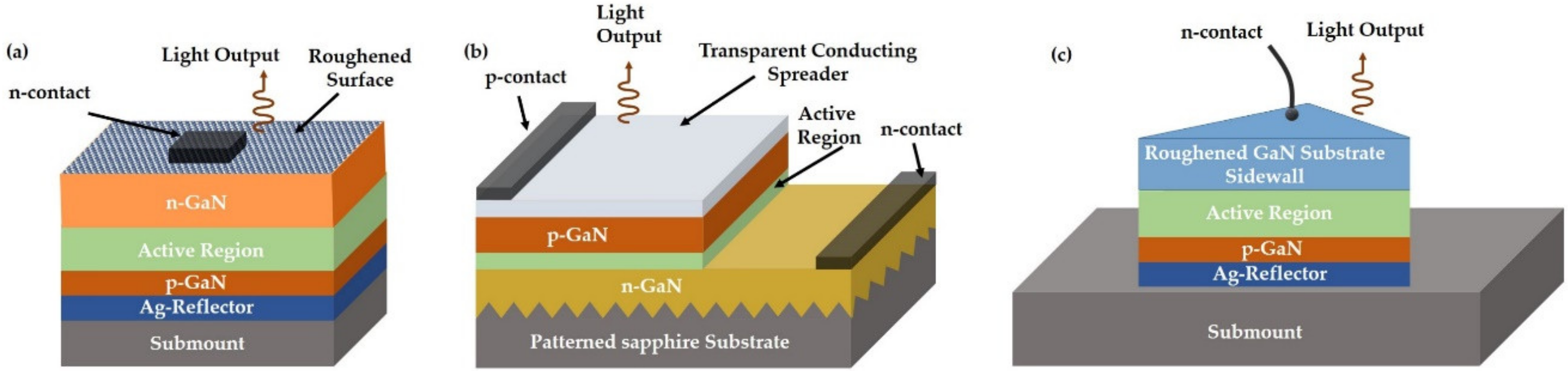
2.3. Next-Generation High-Performance Nitride LEDs

With the development of better-quality substrates, as well as advancements in epitaxial growth techniques [31,32,33,34,35], the focus shifted towards the performance enhancement of nitride LEDs based on low-dislocation density GaN substrates, semi- and non-polar substrates, or patterned sapphire substrates. One of the early works on non-polar, free-standing GaN substrates was published in 2005, which demonstrated a 450 nm LED with an output power of 0.24 mW [36]. A significantly better performing device with a 38.9% EQE and an output power of 23.7 mW was reported in 2007 based on a non-polar m-plane bulk GaN substrate with threading dislocation densities of less than 5 × 106 cm−2 [37]. Since then, research on GaN LEDs based on non- and semi-polar substrates has received a lot of traction. High-performance blue and violet LEDs based on such substrates have already been reported with EQE values of 54.7% and 52.7% respectively [38,39]. Whereas conventional c-plane III-nitrides are characterized by spontaneous and piezoelectric polarization owing to the wurtzite crystal structure’s lack of inversion symmetry, non-polar and semi-polar substrates offer enhanced radiative efficiency, better charge transport, and reduced efficiency droop because of the smaller or nearly-zero polarization effects [40]. In spite of these advantages, the non- and semi-polar GaN LEDs have not been able to replace the conventional c-plane devices primarily owing to the non-availability of low-cost, large-area substrates. The heteroepitaxy of non- and semi-polar GaN epilayers on less-expensive non-native substrates may serve as an alternative, although this is still an active area of materials research because such heterostructures suffer from a significant number of point defects and impurities [41,42], dislocations [43,44], as well as stacking faults [45].
The state-of-the-art GaN LEDs reported so far are based on patterned sapphire substrates (PSS) or quasi-bulk GaN substrates. In 2010, the development of low-power (<100 mW) blue LEDs using PSS was reported by Nichia Corporation. The reported devices had a maximum EQE of 85% and WPE of 81.3% at 20 mA bias current [46]. The development of high-power violet (up to ~800 mW) LEDs with a peak EQE of 73% using low-defect density (~105 cm−2) quasi-bulk GaN substrates was reported by Sora [47]. This device, which could operate at 54% EQE at a very high current density of 1000 Acm−2, enabled Sora’s commercialization of the first 50 W equivalent LED lamp in 2012. The development of a higher-performing violet (λ = 415 nm) LED based on a quasi-bulk GaN substrate, which had a WPE of 84% at an 85 °C operating temperature, was reported in 2015 [48]. Besides the optimization of growth techniques and the utilization of alternative substrates, more recently, significant efforts have been made to enhance the light extraction efficiency (LEE) of nitride LEDs. The LEE of conventional GaN LEDs is relatively low owing to the high refractive index of GaN, which causes a significant fraction of the emitted light to become trapped within the device by total internal reflection (TIR) [49,50]. Three main techniques have been explored to enhance the LEE of nitride LEDs, which are the flip-chip (FC) technique by substrate removal, the utilization of pattered sapphire substrate, or device fabrication based on volumetric bulk GaN substrates.
As shown in Figure 4a, in the FC technique, the LED chip is flipped onto the p-GaN side, bonded onto a submount, and light is collected from the n-side of the device [51,52,53]. Instead of the previously used thin Ni/Au p-contact, a thick layer of Ag is used as the p-contact, which not only facilitates the operation of the device at high current densities, but also serves as a back reflector to increase the LEE of the device. As the refractive index contrast at the GaN–sapphire interface is smaller than the refractive index contrast at the GaN–air interface, light trapping because of TIR is smaller for the FC devices. The LEE of flip-chipped GaN LEDs has been further enhanced by removing the sapphire substrate using an excimer laser, and also by roughening the n-GaN surface to increase the single-pass escape probability of emitted light [53,54]. By positioning both p- and n-contacts on the submount side, the LEE of the so-called vertical injection thin film (VTF) flip-chip design has been extended up to 75–80% [55]. Higher LEE values have been reported with PSS, which uses features such as lines, cones, hemispheres, etc., to further enhance light output (Figure 4b). By incorporating ITO contact with LEDs grown and fabricated on PSS, Nichia Corporation have reported EQEs higher than 84% [46]. More recently LEE values of 90% have been reported using bulk GaN-based volumetric LEDs, which have near-unity vertical-to-horizontal aspect ratios and roughened surfaces not only on the top but also on the sidewalls. Such a geometry significantly reduces lateral loss from sidewall emission and enhances light extraction from the top surface of the device (a representative schematic is shown in Figure 4c) [47,48,56].
A concern related to the degradation of the LEE and electrical performances of GaN-LEDs is current crowding resulting from the low conductivity of the nitride heterostructures [57,58]. This issue is specially related to the large activation energy (~150–210 meV) of Mg-dopants in GaN [59], which results in the low conductivity of p-GaN, and therefore affects uniform current spreading and the extraction efficiency of high-brightness LEDs. An effective means of overcoming this limitation is the incorporation of a modulation-doped AlGaN/GaN heterostructure, which is capable of enhancing the effective hole concentration of the active region [58]. Modulation doping is already an established technique for GaP and GaSb-based LEDs [60,61] and this technique is widely utilized for high-power nitride devices, such as AlGaN/GaN high electron mobility transistors (HEMTs) [62]. The strong polarization field at the AlGaN/GaN interface promotes the formation of sheet carrier densities in the order of 1013 cm−2 in nitrides. In addition to AlGaN/GaN heterostructures, unintentionally doped GaN/p-GaN has also been utilized to increase conductivity by a factor of about 40 [63]. Such enhancement of conductivity significantly improves the current spreading characteristics of nitride LEDs. Modulation doping has also been observed improving the endurance of the device in the face of high electrostatic discharge (ESD) pulses [57,64].

2.4. Nitride-Based White LEDs

It goes without saying that GaN-based LEDs have served as a disruptive technology in the field of lighting and illumination. In fact, the remarkable success of the solid-state lighting (SSL) industry is largely attributed to the advancements made in the development of high-performance nitride LEDs [65,66]. Since the early development of blue-emitting nitride LEDs back in the mid-1990s, significant attention has been given to the realization of white LEDs for visible lighting-related applications. In 1996, Nichia Corporation commercialized the first white LED by combining GaN-based blue LED with Ce: YAG phosphor, which partially absorbs the blue emission and then re-emits a broadband spectrum centered around the yellow wavelength [67,68,69]. Owing to the high efficiency, high stability, and low cost of this technique, it has been the most widely adopted approach by the industry for realizing white LEDs. An alternate approach is to use blue nitride LEDs together with phosphor-converted green and red LEDs, though this approach is limited by the low conversion efficiencies of the green and red phosphors [70]. From a theoretical standpoint, the highest possible luminous efficacies of nitride LEDs (in the range of 300∓400 lm/W) can be achieved by directly combining red, green, and blue (RGB) emitting LEDs onto a single chip [71]. The challenge with this approach is that it necessitates not only high-performance blue LEDs, but also green- and red-emitting nitride LEDs. As commercial red-emitting nitride LEDs have remained elusive owing to their poor performance metrics, the more matured AlInGaP red LED may serve as an alternative for fabricating direct-emission-based RGB arrays. This, however, poses additional challenges, not only in terms of integration, but also in terms of control, as optimizing the operating conditions of LEDs based on two different material systems is rather challenging [72]. Consequently, there has been continued research aimed towards the development of red and green nitride LEDs so that they can be monolithically integrated onto the same chip with blue LEDs.
Different techniques, such as growth optimization of the InGaN-QW with an AlGaN-interlayer [73], doping of the GaN-active region with Europium [74], reduction of in-plane residual stress using thick GaN underlayers [75], and the incorporation of V-pit in the InGaN active region [76], have been employed to attain red nitride LEDs with peak emission wavelengths ranging between 620 nm–633 nm. However, in comparison to state-of-the-art blue and green LEDs, the performance characteristics of these red LEDs are substantially low. In fact, to date, the highest EQE of reported red nitride LEDs is only 2.9% at 629 nm wavelength [73]. While the performance characteristics of red-emitting nitride LEDs need massive improvement, significant improvement needs to be made with InGaN-based green LEDs as well. Green nitride LEDs suffer from efficiency droop, low EQE values, and also high peak current densities at the maximum power point. In fact, the ‘green gap’, which is referred to as the non-availability of efficient green-emitting nitride or phosphor-based LEDs at long wavelengths, has been a long-standing challenge in the field of optoelectronics [65,77,78]. It has been observed that power conversion efficiency decreases and peak efficiency shifts to higher current densities as more indium is incorporated in the active region of the nitride LEDs. Such diminishing characteristics are attributed to the strain developing from the large lattice mismatch between the InGaN (QW)/GaN (barrier) layers [79,80,81], carrier localization resulting from In-composition fluctuation [70], impurities and point defects owing to the low-temperature growth used for indium incorporation [82,83,84], and reduced electron–hole wavefunction overlap in InGaN QWs of high In-composition [85,86].
In spite of these challenges, there have been remarkable improvements in the performance of phosphor-based white LEDs with blue nitride LEDs as the main component. Whereas the first white LEDs reported by Nichia had a luminous efficacy of only 5 lm/W [68,69], white LEDs exceeding 200 lm/W have been developed and commercialized by Cree, Nichia, and Osram since the late 2000s [87]. In fact, Cree already broke the 300 lm/W barrier in 2014 with white LEDs that have correlated color temperature values of 5150 K. In 2017, white LEDs exceeding 200 lm/W were commercialized by Philips [88]. Such remarkable progress of nitride-based white LEDs well exceeds Haitz’s law, which forecasts that every 10 years, the amount of light generated by a LED would increase 10-fold, while the cost per lumen will fall by a factor of 10 [89]. For comparison, the evolution over time of the average cost and light output of nitride-based white LEDs and red LEDs are shown in Figure 5. It is obvious that the advent and development of nitride LEDs has played a major role in enhancing light output while reducing energy costs at the consumer level. The reduced energy cost and carbon footprint of white LEDs have further promoted the market penetration of this technology. According to the latest forecast by the USA Department of Energy (DOE) [90], with further research and development, the transition to white LED sources may result in an annual energy saving of about 569 TWh by the year 2035. This is equivalent to about USD 890 billion in avoided energy costs over the duration of 2017–2035.

2.5. Nitride-Based UV LEDs

Although the development of nitride LEDs has historically been aimed at advancing the field of SSLs, with already remarkable advancements made in this area, the focus has more recently shifted towards new avenues of nitride LED-based research. Among these, the design, growth, and fabrication of nitride-based UV LEDs is currently one of the most promising ones. Research in this area is primarily motivated by the need to create the next generation of UV sources, which may serve as alternatives to toxic mercury lamps and gas lasers for applications related to air and water purification, sterilization, bio and environmental sensing or monitoring, UV curing, plant growth lighting, and phototherapy [91,92]. Since around 2005, AlGaN-based UV LEDs have been extensively studied owing to the tunable bandgap (3.4–6.1 eV) of AlGaN, which covers all three spectral bands of UV radiation, namely UVA (400–320 nm), UVB (320–280 nm), and UVC (280–100 nm). The research outcomes of AlGaN-based UV LEDs, however, suggest that the performance of these devices tends to diminish as the light output shifts from near-UV to deep-UV wavelength. This is primarily owing to the high threading dislocation densities (in the order of 108 cm−2 to 1010 cm−2) arising from the large lattice mismatch at the AlGaN/GaN interface, as the Al mole fraction of the active layer increases [93]. Whereas InGaN-based near-UV (400–365 nm) emitters have performance characteristics similar to those of blue LEDs, with EQEs ranging from 46–76%, the EQEs of AlGaN-based UVB and UVC LEDs have mostly hovered below 10% [91,94,95,96,97,98,99,100,101,102,103,104,105]. The highest performing DUV LED reported so far has had a peak EQE of 20% at an emission wavelength of 275 nm [103]. EQE values of some of the highest reported nitride UV LEDs are shown in Figure 6a for different emission wavelengths covering the UV band.
Research initiatives regarding the further enhancement of the figure-of-merits of UV LEDs are being made on multiple fronts, such as the growth of better quality materials by reducing threading dislocations in AlGaN [93], better n- and p-doping of AlGaN to achieve higher conductivity [106,107,108], design of better contacts and heterostructures for efficient carrier recombination in the active region [92,106,109,110,111], and the application of photon management techniques for enhancing light extraction efficiency [103,104,112,113,114,115,116]. It may be noted that for efficient carrier injection and to prevent carrier overflow from the active region, different heterostructures of DUV LEDs have been explored for band engineering [92]. The most commonly employed heterostructure for a UV LED comprises n- and p-contact layers, GaN/AlGaN multi-quantum wells, n- and p-AlGaN layers for electron and hole injection, and Al-rich, p-doped electron blocking layers to prevent carrier overflow during high injection. The energy band diagram of such a heterostructure is shown in Figure 6b. As p- and n-doping of AlGaN are yet to be optimized, the high-resistivity of Al-rich epilayers make Joule heating an important challenge to overcome for attaining high-performance characteristics in these devices.

2.6. Nitride Based Micro-LEDs

The field of III-nitride micro LEDs has emerged as an important area of research over recent years primarily with the emergence of wearable, portable, and futuristic display technologies, such as smartphones, smartwatches, smartglasses, micro-displays and micro-projectors, augmented reality (AR), and virtual reality (VR) [117,118]. Device dimensions of LEDs used in the backlight of conventional liquid crystal display (LCD) panels are generally kept in the order of millimeters to lessen the effect of efficiency droop. LEDs of 100–200 µm in size are also used as a backlight for LCDs to attain high contrast and high dynamic range (HDR) in the display [119,120]. Micro LEDs, on the other hand, are sub-100 µm (often sub-20 µm) in size, designed specifically for state-of-the-art high-resolution display technologies [118]. The idea of micro LEDs (µLEDs) was first developed by Jiang et al. in early 2000 [121]. In this work, a prototype blue micro-display using InGaN/GaN LEDs was demonstrated with 10 × 10 pixels of 12 µm diameter, and it was predicted that III-nitrides may provide unsurpassed performance metrics in terms of brightness, resolution, contrast, wide-viewing angle, full-color spectrum, long-lifetime, and low-power consumption for small-sized displays. The research and development of III-nitride based µLEDs has since come a long way, and µLED displays have already demonstrated remarkable performance characteristics in terms of high brightness, power efficiency, and HDR [117,118]. In spite of such advancements, there are important issues to be addressed before µLEDs can be commercialized and mass produced. An important concern is the decrease of peak EQE of µLEDs as their dimensions are reduced. The highest reported EQE value of nitride µLEDs is 48.6% for 10 × 10 µm2 arrays [122]. As a matter of fact, EQE values of most reported µLEDs are less than 15% [117]. Consequently, the peak output power per pixel for µLEDs is still low compared to the LEDs being used for SSLs. Such performance degradation is attributed to the increased non-radiative effects resulting from surface recombination and sidewall damage effects, which are less consequential in devices of larger dimensions [123,124]. Another important consideration is that to be able to compete with OLED-based emissive displays, high-performance red, green, and blue LEDs are required on the same chip. This takes us back to the previously referred challenges associated with the green gap. To overcome the green gap-related challenges for µLEDs, techniques such as growth on non-polar and semi-polar substrates [40], the incorporation of AlGaN interlayers in a multi-quantum-well (MQW) active layer [125,126,127], and epitaxially grown disk- or dot-in-nanowires have been proposed [128,129]. A schematic illustration of red-, green-, and blue-emitting nitride nanowires/columns affixed onto the same substrate is shown in Figure 7. Such an array can be grown by selective area growth-based epitaxial techniques, which are more advantageous than the rather time-consuming, resolution-limited, and sidewall-damaging conventional etching-based approach. Furthermore, the epitaxial growth-based approach allows the scaling of RGB LED pixels into small areas of 10 × 10 µm2 or smaller. Another unconventional technique of attaining RGB µLEDs is to use a dilute amount of As or P, or a rare earth element such as Eu, with GaN, which facilitates the tunability of emission wavelengths over the entire visible spectrum [130,131]. More recently, red–green–blue (RGB) 3 × 10 µm2 pixels on the same substrate were developed using nanoring-shaped nitride µLEDs together with CdSe/ZnS red quantum dots, where the nanorings were strain-tuned from blue to green emission [132]. In addition to such device-level improvements, the mass transfer of µLEDs is an important challenge that needs to be addressed [133,134]. This is especially so given the fact that, unlike OLEDs, inorganic nitride LEDs are grown on rigid sapphire or GaN substrates. The mass transfer of these devices from the original substrate to non-native, flexible substrates is rather challenging for flexible display-related applications. Techniques, such as laser lift-off, fluidic assembly, and electrometric stamping, have been employed so far in the quest for cost- and time-effective transfer technologies, while ensuring best possible pixel-control and yield of the devices [133].

2.7. Nitride LEDs for Visible Light Communication

Visible light communication (VLC) systems are considered to be highly promising for next-generation ultra-broadband protocols, especially for indoor applications [40,72,117]. Nitride-based LEDs have played an important role in advancing this area of optical communication technology. In fact, the early demonstrations of VLC in the 2000s were based on nitride LEDs, which were conventional broad area (0.1–1 mm2) devices designed for SSL-related applications. The RC parasitic and slow response time of these large-area devices meant that the achievable data rates were limited up to about 100 Mbps [135]. More recently, the development of sub-100 µm sized LEDs in the form of µLEDs has rejuvenated the field of VLC. The miniaturized chips that are developed with nitride µLEDs yield a small RC time constant, thereby offering high-speed operation with optical bandwidths ranging from several hundred MHz to a few GHz [136,137,138,139,140,141,142,143,144,145]. As shown in Figure 8a, most of these reported devices operate in the green and blue emission wavelengths, though a number of white LEDs have also been utilized to attain data rates in the gigabits/second range [135,136,140,146,147,148,149,150]. The first GHz bandwidth for visible light communication has been reported with cyan LEDs which have InGaN/GaN QW active regions. The nearly two-fold enhancement of electric-to-optical bandwidth, in comparison to previously reported visible LEDs, has been attributed to the lowering of the spontaneous recombination time that has resulted from the aggressive downscaling of the active layer thickness to about ~37 nm [143]. The uniform distribution of injected carriers also has had a positive impact on the high-speed operation of these devices. More recently, a 1.5 GHz modulation bandwidth at 1 kA/cm2 injection current density has been achieved with non-polar m-plane GaN substrate-based InGaN/GaN µLEDs [145]. Such performance enhancement has been attributed to the high spontaneous emission rate resulting from better electron–hole wavefunction overlap in QWs grown on the polarization-free non-polar substrate. The development of high-speed, low-power LEDs for VLC is still an active area of research, and this field is expected to progress further as the modulation bandwidth of nitride LEDs improves. Different techniques, such as the design of resonant cavity nitride LEDs, growth on semi- and non-polar substrates, incorporation of small-area current injection regions, and the fabrication of nanowire-based nitride LEDs, etc., have been proposed and are being explored in this regard [151].

2.8. Temperature Dependence and Reliability of Nitride LEDs

An important consideration related to the operation and performance of III-nitride LEDs is thermal management. Because of the low thermal conductivity and high operating voltage of nitride-based devices, temperature rise resulting from self-heating is observed to have significant influence on the internal and external quantum efficiency of nitride LEDs. Detailed theoretical analyses, combined with experimental measurements, have been conducted on the temperature dependence of the quantum efficiency (QE) of nitride LEDs [152,153,154]. These studies show that the QE of nitride LEDs should decrease with increasing temperatures at low injection current densities because of the temperature dependence of the recombination coefficients. Under high injection conditions, though the QE decreases, the radiative recombination efficiency becomes less dependent on temperature because of the dominance of the Auger process [154]. Self-heating and heat dissipation is observed to have a significant impact on the reliability of nitride LEDs [155,156,157]. It has been reported that nitride LEDs may fail under a few hours of high temperature (250–300 °C) stress because of degradation mechanisms, such as emission crowding and series resistance increase [158,159]. Such degradation has been attributed to the thermally activated interdiffusion of hydrogens and the formation of Mg-H bonds in the p-doped regions [160,161]. To enhance the reliability of nitride LEDs by improving thermal management, techniques such as the incorporation of heat sinks [162,163], flip-chip packaging [164], liquid cooling [165,166], and thermoelectric cooling [167] have been proposed. Very recently, the piezo-phototronic effect has been demonstrated as an effective means of enhanced heat dissipation in nitride LEDs [157] Thermal management continues to be an active area of research and development for the reliable high-temperature operation of nitride LEDs.
Whereas issues such as thermally activated failure mechanisms become important during the high-temperature operation of nitride LEDs, an interesting scenario arises when nitride LEDs are operated close to the cryogenic temperature. Because of the remarkable difference between the activation energy of n- and p-dopants in nitrides (~13 meV for Si dopants and ~150–220 meV for Mg-dopants), asymmetric carrier freeze-out takes place in the n-type and p-type layers of the device heterostructure. This significantly increases the asymmetry of the carrier transport in these devices. Such asymmetry results in the degradation of performance characteristics in the form of high operation voltage [168], low injection efficiency [169], carrier overflow [170] and non-uniform light emission characteristics [171,172]. To overcome these limitations, polarization-induced doping has been proposed, which results in a ~300% enhancement of output light intensity at 4 K compared to the value obtained at room temperature in a deep-UV LED [107,173]. More recently, a bottom-tunnel junction-based inverted LED has been proposed and demonstrated, in which the built-in polarization direction with respect to the direction of the current flow is reversed [174]. Such reversal of the internal field reduces carrier transport asymmetry by limiting electron overflow into the active region of the device. Furthermore, parasitic recombination elsewhere in the device is also reduced in such a design. The overall mechanism, being temperature independent, offers enhanced performance characteristics of nitride LEDs during operation at or near-cryogenic temperatures. It is worth mentioning that the temperature dependence of the material bandgap dictates that cryogenically cooled LEDs will have wider bandgaps than usual. This attribute, together with carrier freeze-out, will further reduce carrier recombination rates at or around cryogenic temperatures. It is important to estimate the recombination rates and the fraction of carrier freeze-out under such conditions to better understand and optimize the cryogenic operation of nitride LEDs.

3. III-Nitride Based Lasers

3.1. Early Development of Nitride Lasers

Stimulated emission and lasing action in GaN-based material systems based on optical pumping were first demonstrated by Dingle et al. in the early 1970s [175]. However, it wasn’t until the 1990s when the first electrically pumped GaN-based laser diode was demonstrated by Nakamura et al. [176]. Materials growth and p-doping-related research endeavors dedicated towards the development of III-nitride-based blue LEDs paved the way for the demonstration of the first nitride laser diode in 1996, which had an output power of 215 mW at 2.3 A forward current and an emission wavelength of 417 nm. The active region of this device comprised InGaN/GaN MQWs, and the waveguide and cladding layers were comprised of GaN and AlGaN, respectively. It is noteworthy that mirrors on the cavity facets of these electrically pumped devices were formed by reactive ion etching (RIE), as cleaving of GaN crystals grown on sapphire was initially found to be challenging because of the presence of multiple cleavage planes of equal strength and within small angular distances [82,177]. Later, as the cleaving of sapphire was optimized by initial thinning and polishing, better-quality mirror facets could be produced. This significantly reduced the emission linewidth of nitride laser diodes (LDs) down to ~0.05 nm [178]. By further enhancing optical confinement, a relatively lower threshold (~4.2 kA/cm2), longer lifetime (~300 h) InGaN/GaN MQW laser was developed in 1997 [179]. In the following subsections, we will discuss the breakthroughs made in the research and development of nitride lasers. The current research trends and prevailing challenges related to thin-film III-nitride lasers will also be discussed in this section. It is to be noted that, considering the practical importance and versatility of applications, the discussions in this review will focus on electrically pumped nitride lasers, which are referred to as laser diodes (LDs) henceforth.

3.2. Performance Enhancement of Blue Laser Diodes

A significant breakthrough in the development of nitride LDs was the utilization of epitaxial laterally overgrown (ELOG) GaN-on-sapphire substrates to reduce the threading dislocation density from 0.1–1 × 1010 cm−2 to around 5 × 106 cm−2 [180,181,182,183]. By using this growth technique, the lifetime of the blue LD was extended beyond 1000 h, and continuous wave (CW) operation with 30 mW output power was achieved at 60 °C [184]. Such enhancements promoted the implementation of nitride lasers on free-standing GaN substrates. These substrates not only offered lower defect densities, but also better thermal properties than the GaN-on-sapphire substrate, and also facilitated the formation of high-quality cleaved facets and n-type back-contacts. An order of magnitude enhancement of output power up to about 200 mW was reported for a blue LD grown on a free-standing GaN substrate [185]. It is to be noted that the device’s heterostructure comprised an Al0.1Ga0.9N/GaN modulation-doped strained-layer superlattice (MD-SLS), which prevented the formation of cracks in the AlGaN cladding that may have otherwise arisen from the difference between the lattice constant and thermal expansion coefficients of AlGaN and GaN [186,187]. Modification of the device dimensions and cavity facets led to further enhancement of output power up to about 500 -MW. A wall plug efficiency (WPE) of 21.6% was also reported in the mid-2000s [188]. By improving packaging and thermal resistance, the output power of these blue LDs was extended beyond 1 W [189]. Watt-class blue (465 nm) LDs with an output power of 5.2 W and a WPE of 37% were developed on conventional c-plane GaN substrates [190]. Around the same time, by improving carrier and optical confinement, blue (442 nm) LEDs with WPE values of 40.5% were reported with an output power exceeding 5 W [191]. Follow up of this work led to the development of a 455 nm blue LD with an output power of 5.34 W and a WPE of 43.4% under CW operation [191]. More recently, state-of-the-art blue LDs with an output power of 5.67 W with a peak WPE of 49.1% have been reported under CW operation [192]. Gradual improvement of the WPE of some of the best performing blue laser diodes is shown in Figure 9a. As far as the reliability is concerned, state of the art nitride LDs have lifetimes ranging from between 10,000 to 20,000 h [190,193]. Recently, it has been shown that, by optimizing the growth condition of electron blocking layers, dislocation densities in these devices can be reduced from about 108 cm−2 to 105 cm−2 [194]. This resulted in a nearly five-fold enhancement of the lifetime of blue LDs (from ~2000 h to about 100,000 h). These studies suggest a direct correlation between the degradation rate and the defect density of nitride LDs.

3.3. Nitride-Based Long-Wavelength Laser Diodes

The steady progress in the improvement of the performance characteristics of III-nitride blue LDs has been accompanied by research efforts aimed towards the development of longer-wavelength nitride laser diodes. The design of longer-wavelength nitride LDs, however, requires higher indium content in the active region, which leads to issues such as the degradation of material quality, owing to higher strain in the GaN/InGaN active region, enhancement of the piezoelectric field and the consequent smaller overlap between electron–hole wavefunction, the broadening of spontaneous emission spectra resulting from reduced layer homogeneity in the In-rich active region, and also the formation of non-radiative recombination centers during materials growth owing to the higher vapor pressure of InN compared to GaN. Another area of concern related to nitride lasers is the optical field loss because of the relatively small refractive index contrast between the waveguiding and cladding layers of these heterostructures [199,200]. Altogether, these issues significantly reduce the modal gain of long-wavelength nitride LDs and also their lasing thresholds [197]. A summary plot of threshold current density vs. the lasing threshold of reported nitride LDs illustrates this point (shown in Figure 9b). In spite of the abovementioned challenges, significant developments have been made with green (515–535 nm) LDs since their early development in 2009–2013 [195,196,201,202,203]. The first watt-class green laser, with an emission wavelength of 520 nm, was reported by Nichia on a conventional c-plane GaN substrate in 2012 [204]. Another watt-class laser of the same wavelength and with a WPE of 13% at around room temperature under CW operation was reported by OSRAM in 2014 [191]. A 532 nm green LD with a higher output power of 2 W was reported in 2017 on free-standing semipolar GaN substrates [190]. State-of-the-art green LDs with emission wavelengths of 525 nm and 532 nm reportedly have an optical output power ranging from 1.2 to 1.8 W, with WPEs of 18–21% [192,205]. Wall plug efficiency values of some of the reported high-performance green LDs are compared with the WPE values of blue LDs in Figure 9a. Though these characteristics are inferior compared to the performance metrics of state-of-the-art blue nitride LDs, it is envisaged that continued research and development initiatives will further enhance the characteristics of long-wavelength LDs. As will be discussed later, over the last few years, nitride lasers extending from red to NIR regions have been developed based on nanostructures, such as nanowires and quantum dots. These developments should go a long way to meet the demand for high-performance RGB LDs for applications related to large laser projectors, digital cinema projectors, and projectors for televisions and smart devices.

3.4. Nitride Based Ultraviolet Laser Diodes

As has been discussed in Section 2, nitride material systems are already under extensive investigation for the development of UV emitters in the form of nitride LEDs. However, for applications such as free-space non-line-of-sight communications, sensing, remote disinfection, and biomedicine, UV lasers are undoubtedly more suitable than their LED counterparts [206]. Nitride LDs are unmistakably considered to be the most promising candidates for the development of semiconductor lasers that can cover all three bands of the UV spectrum. To date, a number of groups have experimentally realized nitride LDs with emission wavelengths in the UVA band. These devices have been designed with InGaN, InAlGaN, or AlGaN MQW active regions. Among these, the lowest threshold has been achieved with the InGaN active region [191,207,208,209,210,211,212,213,214,215,216,217]. The emission wavelength of InGaN-based UV LDs, however, is fundamentally restricted within 367–400 nm. In fact, until 2003, all reported nitride-based UV LDs had emissions above 365 nm [207,208,218], which corresponds to the band-to-band emission wavelength of bulk GaN. The first realization of a sub-365 nm UV LD, reported by Kneissl et al., was based on Al0.02Ga0.98N MQW, comprised of InAlGaN barrier layers [211]. The reported device had an emission wavelength of ~360 nm and a minimum threshold current density of 23 kA/cm2 at room temperature. By increasing Al-content in the active region, the emission wavelength of the LD was lowered down to 336 nm by Yoshida et al. [214]. Experimental realization of nitride LDs of smaller wavelengths, however, remained a long-standing challenge for about a decade, primarily because of epitaxial growth, n-/p-doping, electrical contact formation, and facet formation-related complexities associated with Al-rich heterostructures. Threshold current density, therefore, tends to increase as the emission wavelength shifts towards the DUV region (as shown in Figure 9b). Though a high-power UV LD with a peak output of 1 W was developed in 2015, the emission wavelength of the device (~338 nm) was still within the UVA band [217].
The development of the first ever thin-film nitride LD that could operate in the UVC range was reported rather recently in 2019 [219]. The device heterostructure, comprised of AlGaN MQW, cladding, and waveguiding layers, was grown on a single-crystal AlN substrate, and, consequently, issues related to dislocation or crack formation were successfully overcome. Under a pulsed operation, the threshold current density of this device was recorded to be 25 kA/cm2. More recently, UVB laser diodes of λ = 298 nm have been demonstrated on AlN/sapphire templates with a composition-graded p-AlGaN cladding layer. The reported device had a threshold current density of 67 kA/cm2 at room temperature under pulse operations [220]. A UVB laser of a lower threshold (~25 kA/cm2) was reported by the same group using an Al0.6Ga0.4N/AlN/sapphire substrate [221]. A 279 nm UVC nitride laser of an even smaller threshold current density (~19.6 kA/cm2) was also reported in 2020 [219]. These recent developments of thin-film nitride-based UV LDs have been closely accompanied by research efforts dedicated towards the development of III-nitride nanowire-based UV LDs. In fact, AlGaN nanowires grown on silicon have already been utilized to realize room temperature, electrically pumped UVC lasers with λ = 239 nm [222]. Just as semiconductor-based LDs emitting in the visible and NIR wavelengths have found widespread applications because of their high efficiency, long-lifetime, small form factors, and robustness, it is expected that with further development, nitride-based UV lasers will also become viable alternatives to traditional UV laser sources, such as excimer lasers, argon ion lasers, He-Cd lasers, 3rd/4th harmonic mediated Nd: YAG lasers, or nitrogen lasers—all of which invariably suffer from limitations, including low-efficiency, heating, toxicity, high-voltage requirements, and limited lifetimes [198].

3.5. Nitride-Based VCSELs

Even though the vertical-cavity surface-emitting laser (VCSEL) is a matured technology for III-V materials, such as GaAs and InP, III-nitride VCSELs are effectively still in their early stages of development. In fact, the first electrically pumped nitride VCSEL was reported only in 2008, which is about a decade after the edge-emitting blue nitride lasers were commercialized [223,224]. The schematic diagram of a typical nitride edge-emitting laser is shown in Figure 10a. As can be observed, this structure is rather convenient to produce using epitaxial growth, while the mirror facet can be formed by cleaving. The later arrival of nitride VCSELs is attributed to several material growth and fabrication-related challenges associated with the practical realization of these devices. Whereas high-quality distributed Bragg reflector (DBR) mirrors are routinely produced in GaAs-based VCSELs using alternate pairs of epitaxially grown AlGaAs/GaAs, the large lattice mismatch between AlGaN/GaN precludes the production of such high-quality mirrors. Furthermore, the small refractive index contrast between AlN and GaN necessitates the growth of a large number of DBR pairs for nitride VCSELs, which makes material growth even more challenging. Consequently, nitride VCSELs are designed either with hybrid reflectors, which are comprised of an epitaxial mirror on one side and dielectric mirrors on the other side (as shown in Figure 10b), or with dual-dielectric reflectors comprised of dielectric DBR mirrors both at the bottom and on top of the heterostructure (as shown in Figure 10c). Different dielectric combinations, such as SiO2/TiO2 [225], SiO2/Nb2O5 [226], Ta2O5/SiO2 [227], have been reportedly utilized for realizing DBR mirrors of nitride VCSELs. Poor current spreading because of the relatively large contact resistance of p-GaN is another area of concern for realizing nitride VCSELs. This issue is commonly addressed by employing an intracavity contacted structure, in which highly transparent and conductive oxides such as ITO are formed between the p-GaN and the DBR mirror so that holes are injected laterally into the active region. This, to some extent, mitigates current crowding and increases the overlap between carrier recombination centers and the optical mode profile [223]. More recently, it has been shown that the tunnel-junction current spreading layer, instead of the ITO, can further reduce threshold current density and the operating voltage of nitride VCSELs [228,229,230,231]. ITO-based current spreading layers, however, are unsuitable for operation in the UV region because of the high absorption coefficient of this material below the visible wavelength range. To overcome this limitation, a modulation-doped short-period super-lattice structure has been proposed for nitride-based UV VCSELs [232]. The holes in this device are expected to encounter less ionized impurity scattering in the unintentionally doped narrow bandgap region. This should minimize scattering-mediated absorption losses during the buildup of photon roundtrip gain in the active region of these devices.
Another challenging area related to the development of nitride VCSELs is the attainment of lateral optical confinement (LOC). In commercial GaAs VCSELs, selective lateral oxidation is conveniently achieved by lateral oxidation of the high Al-content AlGaAs layer. As this technique is not applicable to AlGaN, nitride VCSELs are prone to anti-guiding effects which result in high optical losses and consequently high threshold gains [233]. To enhance the LOC of nitride VCSELs, techniques such as the incorporation of ion-implanted aperture [234] or photochemically etched air-gap aperture [235] have been attempted. More recently, nitride VCSELs with LOC structures have been developed which employ a buried SiO2 layer beneath the epitaxial layers [225,236]. In another work, a curved mirror has been monolithically formed on a GaN wafer to limit light diffraction [227]. This approach allows the realization of a longer cavity VCSEL, which has a smaller threshold current density. In spite of these recent signs of progress, significant performance enhancement of nitride VCSELs is required, especially in terms of threshold current density and output power. As VCSELs can be conveniently fabricated as a 2D array of devices which can emit light from the top in unison, blue nitride VCSEL lasers are considered to potentially be highly suited for applications related to VR/AR displays and micro-projectors. Watt-class blue VCSEL arrays with high-quality far-field beam patterns have recently been developed for such applications [226]. It is envisaged that the scope of nitride VCSELs will broaden further as devices of higher output power density, tunable spectral ranges, and lower threshold current densities are developed.

4. Next-Generation Nitride Emitters

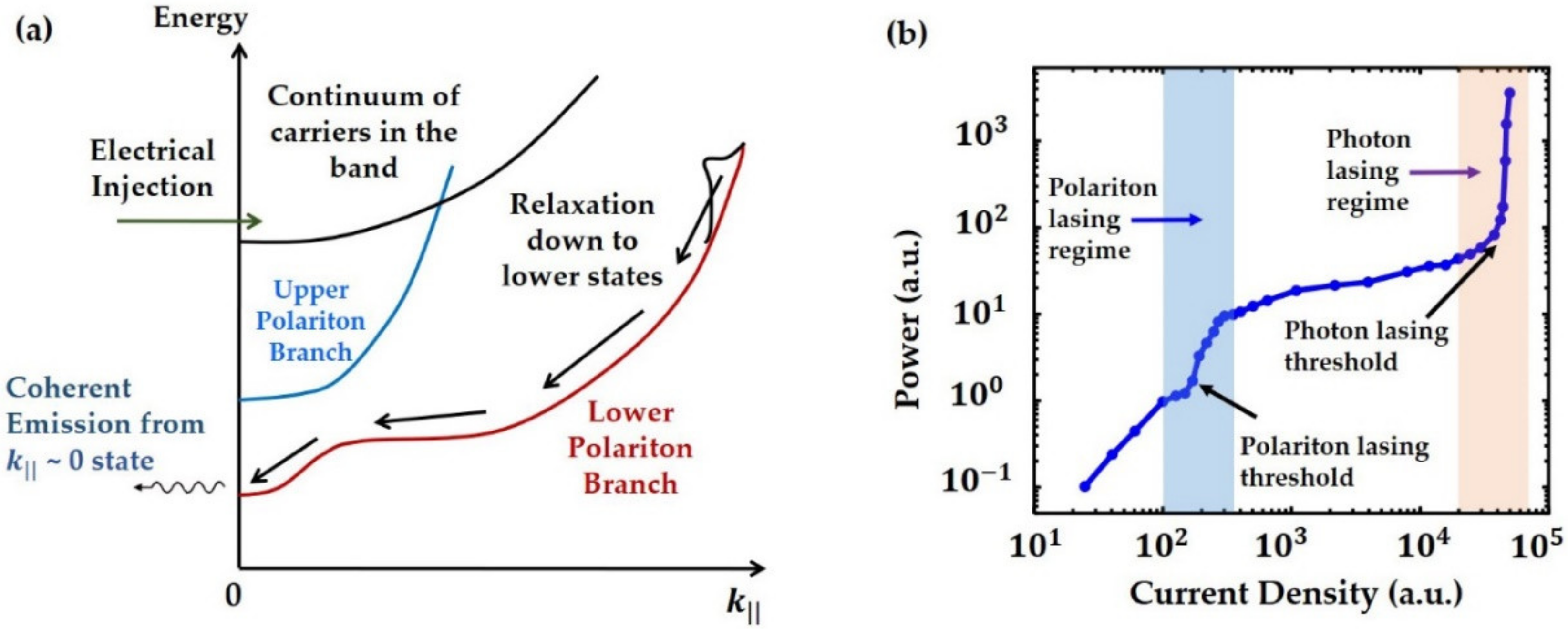
4.1. Nitride-Based Exciton-Polariton Lasers

Exciton-polariton lasers are a new class of coherent emitters that operate based on the principle of the stimulated scattering of light matter-coupled Bosonic quasi-particles, known as polaritons. When an emitter in the form of bulk, quantum well, quantum wire, or quantum dot is placed inside a suitably designed microcavity, the strong interaction between the optical modes and the exciton states gives rise to new eigenstates in the form of exciton-polaritons. The typical dispersion relation of the exciton-polariton is shown in Figure 11a, where a coherent population of polaritons builds up at the k | | = 0 point of the lower polariton (LP) branch under optical or electrical pumping. The possibility of generating coherent light by spontaneous radiative recombination from a coherent exciton-polariton condensate in a semiconductor microcavity was first proposed by Imamoglu et al. in 1996 [237]. The separation of stimulation and emission in a polariton device ultimately results in coherent emission without population inversion. Hence, it is expected that the threshold energy required for coherent emission from this device would be much smaller (about one to two orders lower) than that of a photon laser [237,238,239] (a schematic illustration of two-threshold lasing in a polariton device is shown in Figure 11b). For this reason, polariton lasers are considered to be highly promising low-power, coherent light sources for medical and biomedical applications, high-speed optical interconnects and photonic-integrated circuits, all-optical routers and switches, and quantum information processing [240,241,242,243].
Advancements in the areas of epitaxial growth and device fabrication techniques have already led to several realizations of this novel coherent light source based on different material systems. Because of the relatively matured growth and fabrication techniques, GaAs had been the preferred material of choice for the early development of polariton lasers, and the first electrically pumped polariton lasers were demonstrated using the GaAs-VCSEL structure in 2012 [244,245]. The operation of these devices, however, was limited to cryogenic temperatures because of the low exciton-binding energy of the material system. Wide bandgap materials, such as GaN and ZnO, appeared to be strong contenders in this regard owing to their high exciton-binding energies and oscillator strengths, which meant that excitons in these material systems would not dissociate at room temperature, if not higher [246,247]. As far as electrical pumping is concerned, GaN has been considered to be more promising than ZnO because of the advancements made with epitaxial growth, p-doping, and fabrication of nitride material systems.
Because polariton lasing inevitably requires high-quality microcavities with dimensions in the order of emission wavelength, GaN-based polariton lasers were initially attempted with the VCSEL structure. In fact, the first room-temperature polariton lasing was reported to employ an optically pumped bulk GaN emitter, which was sandwiched between high-quality SiN/SiO2 and AlInN/AlGaN DBR mirrors to form a vertical cavity surface-emitting structure [248]. In spite of this milestone, experimental realization of an electrically pumped room-temperature polariton laser remained elusive, primarily because of the high resistivity of a large number of lattice-mismatched epitaxial pairs in the DBR mirror. In order to circumvent the limitations of the GaN-based surface-emitting structure, an edge-emitting structure has been regularly employed for creating electrically pumped polariton devices, where bulk GaN is used as the active region and SiO2/TiO2 DBR mirrors are formed on both sides of the structure [249,250,251,252]. The device structure, the schematics of which are shown in Figure 12, may be viewed as an in-plane VCSEL or a very short-cavity Fabry–Pérot laser, where optical feedback and current injection are orthogonal to each other. Based on this novel structure, the first electrically pumped polariton LD, which could operate at room temperature, was developed in 2014 [249]. This bulk GaN-based device had a threshold current density of 169 A/cm2, which was several hundred times smaller than the threshold current density of photon lasing obtained from the same device. This work was followed by the first experimental demonstration of the small-signal modulation response of a polariton laser diode. A maximum −3 dB modulation bandwidth of 1.18 GHz was obtained from these measurements [250]. It is to be noted that the emission wavelength of these polariton laser diodes is around the GaN band-edge of 365 nm, i.e., in the UVA region of the EM spectrum. With further development, these low-threshold, low-power, UV-coherent emitters undoubtedly hold great potential for applications, including biochemical analysis, photo-alignment of nematic liquid crystals, eye surgery, sensing, etc. [71,253,254,255,256,257]. III-nitride polariton lasers continue to be an active area of research. Very recently a ridge waveguide polariton laser with ultra-short Fabry–Perot ridge cavities (5–60 µm) have been demonstrated to be promising for integrated phonics-related applications [258].

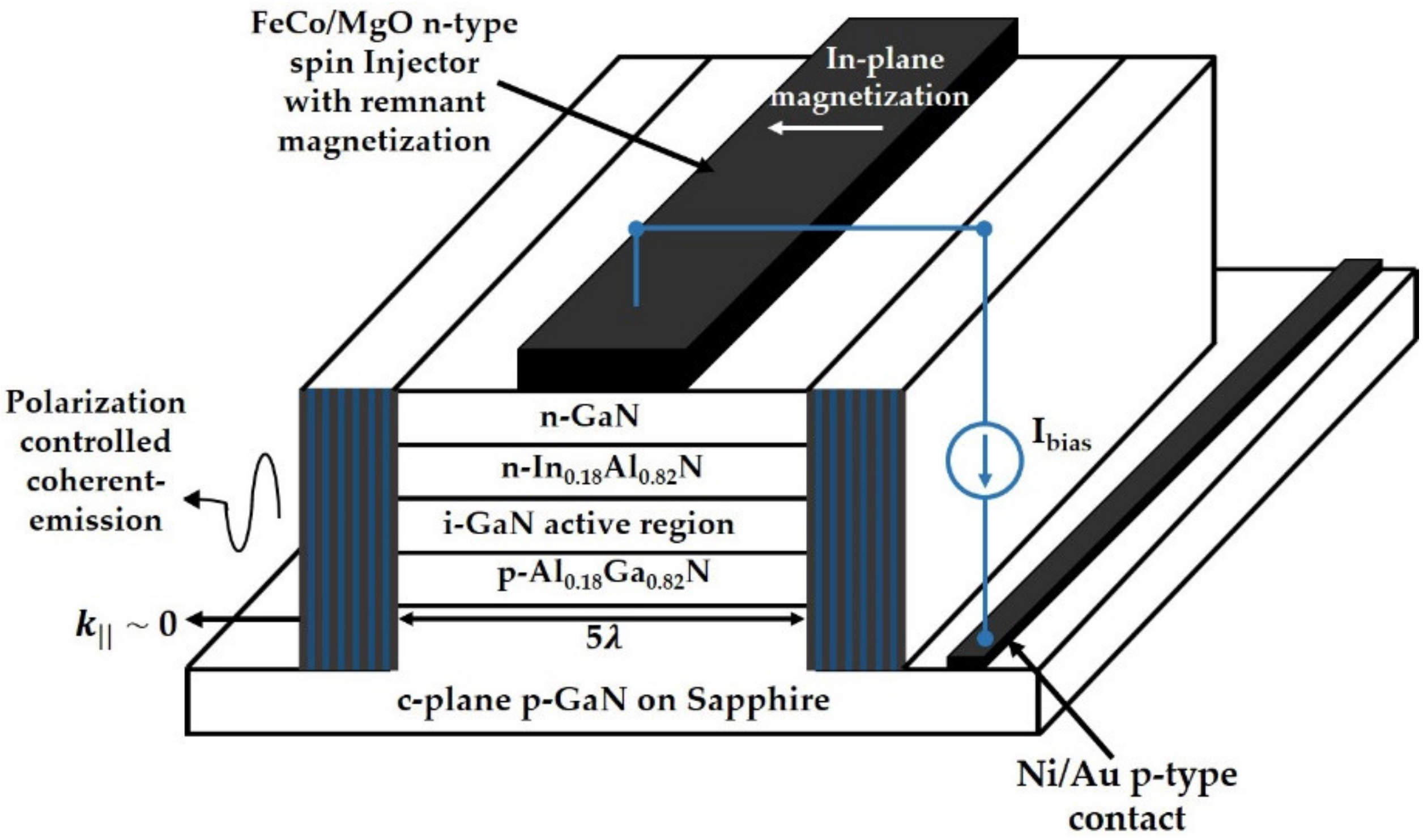
4.2. Nitride-Based Spin LEDs and Lasers

An electrically pumped light-emitter, in which circular polarization of the output light can be appreciably controlled, is useful for a plethora of applications, such as the preparation of chiral compounds and chiro-optical spectroscopy of biochemically active molecules, non-invasive medical diagnosis, optical information processing, image projection, and display applications, including reconfigurable optical interconnects, ultrafast optical switches, cryptographic optical communications, and telecommunications with enhanced bandwidth [252,259,260,261,262,263]. Spin-LEDs and –lasers are considered to be viable means for attaining such control over the polarization degree of freedom of light. The operation of both these optoelectronic devices is governed by the spin selection rules, which dictates the transfer of spin information of injected carriers to the output circular polarization of light. The majority of spin-optoelectronic devices, realized with GaAs material systems, operate in the NIR region of the spectrum [259,260,261]. However, ever since the last decade, there has been a growing interest in the research of nitride-based spin-LEDs and spin-LDs, which are capable of emitting circularly polarized light under electrical injection at room-temperature.
The first nitride LEDs were reported in 2005–2006, which used transition metal dilute magnetic semiconductor (DMS) GaMnN as the spin injector [264,265]. In spite of the ferromagnetic nature of the alloy, the output degree of polarization of the device was low (<1%). Similar values of circular polarization were reported with a near-visible spin-LED, which had an InGaN/MQW active region and a (Ga, Mn)N DMS spin injector. A spin-LED with higher values of circular polarization (6% at 5 K and 2.5% at 200 K) was reported with n-type GaCrN as the spin injector. The emission wavelength of this device was 410 nm [266]. A major breakthrough was made in 2014, when the first nitride-based spin-LED was reported with a 10.9% circular polarization at room temperature, under a low magnetic field of 0.35 T [267]. The 300 nm diameter InGaN/GaN multiple quantum disk device used Ni-ferromagnetic contact and Fe3O4 magnetic nanoparticles, which enabled the selective transfer of spin-polarized electrons with the disks, thereby increasing the number of electrons which had preferred spin orientation in the multi-quantum-disks. The follow-up to this work led to the development of the first nitride spin laser, which exhibited 28.2% spin polarization at room temperature under a low magnetic field of 0.35 T [262]. The reported optically pumped device used GaN nanorods of ~200 nm diameter and Fe3O4 nanoparticles for spin transfer. Optical feedback in the device was attained using whispering gallery resonant modes formed at the periphery of the GaN nanorods.
Circular polarization in the absence of a magnetic field was reported with a GaN-based edge-emitting spin-LED, which utilized remnant magnetization of the n-type FeCo/MgO spin contact [263]. Using similar spin-contacts, the first spin-polariton laser was developed in 2017, which exhibited 25% circular polarization under remnant magnetization at room temperature. A schematic illustration of this device is shown in Figure 13. Whereas the threshold current density of previously reported spin VCSELs ranged from 2–8 kA/cm2 [259,260], the reported electrically pumped spin-polariton lasers could operate at an ultra-low threshold of ~69 kA/cm2, primarily owing to the co-existence of polariton lasing and spin-transfer phenomena. In spite of the smaller spin-orbit coupling and about an order of magnitude shorter spin-relaxation time compared to the GaAs material system, a robust spin-dependent gain was obtained for wurtzite GaN at room temperature. Such characteristics are considered to be highly conducive for realizing robust, electrically pumped spin lasers. Moreover, it has been predicted that with further development, nitride spin-lasers can far exceed the performance of conventional photon lasers, and may serve as a workhorse for ultrafast operations [268].

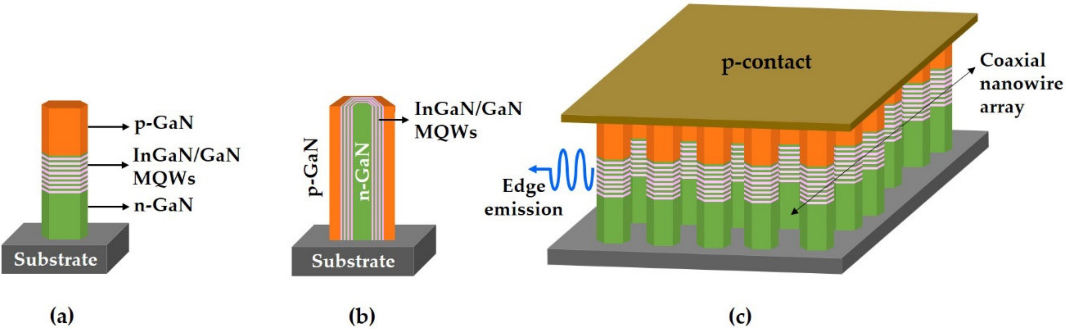
4.3. Nanostructured Nitride Emitters

In spite of the tremendous progress made with material growth, the performance of conventional thin-film III-nitride light emitters is severely limited by problems associated with large dislocation densities of the starting substrate, lattice-mismatched epitaxial growth, and the strain-induced piezoelectric polarization field. Furthermore, challenges associated with the incorporation of high indium content precludes the realization of high-performing nitride emitters in the long-wavelength region. It is expected that many of these challenges can be appreciably overcome by employing nitride nanostructures, such as nanowires, nanorods, disk-/dot-in-nanowires, and self-organized quantum dots [269,270,271]. Among these nanostructures, III-nitride nanowires are considered to be one of the most promising candidates for realizing the next generation of nitride emitters. The radial stress-relaxation mechanism associated with the large surface area of III-nitride nanowires results in remarkably small dislocation densities (in the order of 102 cm−2 or smaller), as well as reduced piezoelectric polarization fields. Furthermore, employing patterned or self-organized growth, the emission wavelength of In(Al)GaN nanowires can be tuned from the DUV to the NIR region of the spectra. Carrier confinement in III-nitride nanowires can be attained in axial or radial directions, depending on the coaxial or core-shell structure of the nanowires (shown in Figure 14a and Figure 15b respectively). These nanowires can be grown in the form of a self-organized, uniform random array, or in the form of a periodic array (as shown in Figure 14c) using selective-area growth techniques. In addition to these, low-dimensional systems in the form of quantum dots, disks, and wells can be conveniently incorporated in the active region of nitride nanowires to attain strong carrier confinement. From the photonic point of view, strong optical confinement—even in the form of Anderson localization—can be attained in III-nitride nanowires, and such confined modes can be conveniently tuned by controlling geometrical aspects of these nanostructures [222,272].
The mentioned exotic electrical and optical properties have encouraged the experimental realization of numerous LEDs and electrically pumped lasers based on III-nitride nanowires. Particularly with the recent drive towards the development of µLEDs for the next generation of displays, there has been growing interest in developing InGaN/GaN nanowire-based on-chip RGB LEDs [128,129]. Another major advantage of III-nitride nanowire-based light emitters is that these nanostructures can be grown on silicon substrates with little or no-strain [270,273]. This offers the prospect of monolithic integration of nitride emitters in the form of LEDs or lasers for future high-speed optoelectronic integrated circuits (OEIC). In fact, a monolithic III-nitride photonic integrated circuit comprising a 1.3 µm InGaN/GaN nanowire-array laser has already been demonstrated on (001) silicon substrate [274]. Similar nanowire arrays have been utilized to successfully develop edge-emitting nitride LEDs and lasers extending from red to 1.3 µm emission wavelengths [275]. These lasers represent the handful examples of long-wavelength nitride emitters, which have been otherwise extremely difficult to obtain with conventional thin-film nitride epitaxy. Besides long-wavelength operation, operation in the UV and DUV regions has also been successfully demonstrated using nitride nanowire-based LEDs and laser diodes. This is owing to the fact that the radial strain-relaxation mechanism of nanowires allows the growth of significantly better quality AlGaN/GaN heterostructures compared to the structures grown by thin-film epitaxy. In addition to the conventional edge-emitting structures, high-quality-factor resonant micro- or nano-cavities in the form of Fabry–Perot lasers [276,277], plasmonic lasers [278,279], photonic-crystal lasers [280], micro-stadiums [281], and ring-cavity [282] lasers have been designed and experimentally demonstrated using InGaN/GaN nanowires. In spite of these significant achievements, a number of challenges need to be overcome to make nitride nanowire-based emitters mature enough for commercial, widespread utilization. The doping and electrical contact formation of nitride nanowires need further optimization to improve the conductivity and reliability of the devices. The non-radiative recombination associated with surface states of these nanowires also needs to be mitigated to enhance the output power and efficiency of these devices. More detailed reviews of III-nitride nanowire-based LEDs and lasers are available in [269,270,271].
Besides III-nitride nanowires, self-organized InGaN/GaN quantum dots (QDs), grown by Stranski–Krastanow or Volmer–Weber growth techniques have also been utilized for the successful development of III-nitride emitters. The strain-relaxation mechanism-based growth technique of QDs significantly reduces the piezoelectric field in the active region of these heterostructures, which usually comprise several layers of QD arrays [283,284]. Non-radiative recombination is also significantly reduced because carriers are quantum-confined within these quasi-three-dimensional nanostructures, and therefore cannot easily migrate to the trap centers. These attributes have aided the experimental realization of high-performance red-emitting (λ = 630 nm) nitride lasers, where multiple layers of InGaN/GaN quantum dots were incorporated (shown in Figure 15a) by molecular beam epitaxial growth [285]. The threshold current density of these devices is around 1.6 kA/cm2, which is one of the lowest for long-wavelength nitride lasers. Very recently, an external quantum efficiency of 18.2% has been obtained for green µLEDs based on self-assembled InGaN quantum dots. This value is about two times higher than the EQE values reported for conventional quantum well-based green µLEDs [286]. Polarized single-photon emission, which is highly desirable for quantum cryptography-related applications, has also been attained from an electrically driven single InGaN/GaN dot-in-nanowire single-photon emitter (a schematic illustration of the device shown in Figure 15b) [287]. These results suggest that nitride nanostructures hold significant promise for realizing next-generation emitters, particularly for applications where performance characteristics of thin-film nitride devices are rather limited. Consequently, the design, growth, and experimental realization of nanostructured-based nitride emitters continue to be a highly active areas of research.

5. Conclusions

In summary, a comprehensive review of III-nitride-based light-emitting electrically pumped devices, i.e., LEDs and lasers, have been presented in this work. A scientific exploration that started in the early 1970s with the aim of developing a working blue-emitting optoelectronic device, culminated in the practical realization of a technology that changed the landscape of an entire industry, namely the solid-state lighting industry. Further scientific explorations and engineering ventures based on III-nitride emitters have led to the emergence of a plethora of novel avenues of research which have flourished immensely in the already rich field of photonics and optoelectronics research. The present review, within its limited scope, provides an overview of this tremendous progress of nitride-based emitters, and also points out the directions towards which research in this area is heading. It should be noted that this review touches on almost all topics relevant to the research and development of III-nitride-based LEDs and lasers, a topic that has not been discussed so far is the emerging field of research on boron nitride (BN)-based light emitters. Boron nitride, in particular its 2D variant known as hexagonal BN (h-BN), holds tremendous potential for optoelectronic applications owing to its wide bandgap (~6 eV) nature with good radiative recombination properties [288,289,290], atomically smooth surfaces [291], and suitability for Van der Waals epitaxy [292]. The unique electronic and optical properties of h-BN offer emission both in the visible and UV regions [293,294,295,296], with high brightness, controllability of output polarization, and tunable emission characteristics [297]. By controlling defect-mediated color centers of h-BN, a number of nitride-based single-photon emitters have already been reported since 2016 [293,296,298,299,300]. These emitters are deemed to be highly suitable for applications related to quantum sensing, quantum information processing, and quantum communication. By exploiting the acceptor-like Boron vacancy formation in h-BN, Mg-dopant free III-nitride deep-UV LEDs with an emission wavelength of 210 nm and an electrical efficiency of 80% have also been developed [295]. Research on III-nitride thus continues to evolve and flourish with the continued development of materials growth techniques, fabrication technologies, and measurement systems. As Niels Bohr is famously quoted saying, “Prediction is very difficult, especially if it’s about the future!”, it is always difficult to foretell which next-generation nitride emitters will pass the test of time and become mature enough to become a commercial success. However, looking back into the exemplary rise of blue nitride LEDs, it can be safely surmised that nitride light-emitting devices will significantly impact the photonics and optoelectronics related technological evolution of the 21st century.

Author Contributions

Conceptualization, M.Z.B. and A.A.; writing, M.Z.B.; review and editing, S.A. and A.A.; figure preparation and schematic illustration, S.A.; literature review and data collection, M.Z.B. and B.S.; referencing, B.S. All authors have read and agreed to the published version of the manuscript.

Funding

This research received no external funding.

Institutional Review Board Statement

Not applicable.

Informed Consent Statement

Not applicable.

Data Availability Statement

Not applicable.

Acknowledgments

M.Z.B. and B.S. acknowledge the support of the Department of Electrical and Electronic Engineering, Bangladesh University of Engineering and Technology (BUET).

Conflicts of Interest

The authors declare no conflict of interest.

References

  1. Zhou, C.; Ghods, A.; Saravade, V.G.; Patel, P.V.; Yunghans, K.L.; Ferguson, C.; Feng, Y.; Kucukgok, B.; Lu, N.; Ferguson, I.T. The Current and Emerging Applications of the III-Nitrides. ECS J. Solid State Sci. Technol. 2017, 6, Q149. [Google Scholar] [CrossRef] [Green Version]
  2. III-Nitride Semiconductor Optoelectronics, Volume 96—1st Edition. Available online: https://www.elsevier.com/books/iii-nitride-semiconductor-optoelectronics/mi/978-0-12-809584-3 (accessed on 15 August 2021).
  3. Manasreh, M.O. III-Nitride Semiconductors: Electrical, Structural and Defects Properties; Elsevier: Amsterdam, The Netherlands, 2000. [Google Scholar]
  4. Maruska, H.P.; Tietjen, J.J. The Preparation and Properties of Vapor-Deposited Single-Crystal-Line GaN. Appl. Phys. Lett. 1969, 15, 327–329. [Google Scholar] [CrossRef]
  5. Pankove, J.I.; Miller, E.A.; Berkeyheiser, J.E. GaN Blue Light-Emitting Diodes. J. Lumin. 1972, 5, 84–86. [Google Scholar] [CrossRef]
  6. Pankove, J.I. Low-Voltage Blue Electroluminescence in GaN. IEEE Trans. Electron Devices 1975, 22, 721–724. [Google Scholar] [CrossRef]
  7. Boulou, M.; Furtado, M.; Jacob, G. Light-Emitting Diodes Based on GaN. Philips Tech. Rev. 1977, 37, 237–240. [Google Scholar]
  8. Maruska, H.P.; Rhines, W.C.; Stevenson, D.A. Preparation of Mg-Doped GaN Diodes Exhibiting Violet Electroluminescence. Mater. Res. Bull. 1972, 7, 777–781. [Google Scholar] [CrossRef]
  9. Lagerstedt, O.; Monemar, B.; Gislason, H. Properties of GaN Tunneling MIS Light-emitting Diodes. J. Appl. Phys. 1978, 49, 2953–2957. [Google Scholar] [CrossRef]
  10. Kawabata, T.; Matsuda, T.; Koike, S. GaN Blue Light Emitting Diodes Prepared by Metalorganic Chemical Vapor Deposition. J. Appl. Phys. 1984, 56, 2367–2368. [Google Scholar] [CrossRef]
  11. Mandel, G. Self-Compensation Limited Conductivity in Binary Semiconductors. I. Theory. Phys. Rev. 1964, 134, A1073–A1079. [Google Scholar] [CrossRef]
  12. Amano, H.; Sawaki, N.; Akasaki, I.; Toyoda, Y. Metalorganic Vapor Phase Epitaxial Growth of a High Quality GaN Film Using an AlN Buffer Layer. Appl. Phys. Lett. 1986, 48, 353–355. [Google Scholar] [CrossRef] [Green Version]
  13. Amano, H.; Akasaki, I.; Hiramatsu, K.; Koide, N.; Sawaki, N. Effects of the Buffer Layer in Metalorganic Vapour Phase Epitaxy of GaN on Sapphire Substrate. Thin Solid Film. 1988, 163, 415–420. [Google Scholar] [CrossRef]
  14. Akasaki, I.; Amano, H.; Koide, Y.; Hiramatsu, K.; Sawaki, N. Effects of Ain Buffer Layer on Crystallographic Structure and on Electrical and Optical Properties of GaN and Ga1−xAlxN (0 <x ≦ 0.4) Films Grown on Sapphire Substrate by MOVPE. J. Cryst. Growth 1989, 98, 209–219. [Google Scholar] [CrossRef]
  15. Nakamura, S.; Mukai, T.; Senoh, M. In Situ Monitoring and Hall Measurements of GaN Grown with GaN Buffer Layers. J. Appl. Phys. 1992, 71, 5543–5549. [Google Scholar] [CrossRef]
  16. Amano, H.; Kito, M.; Hiramatsu, K.; Akasaki, I. P-Type Conduction in Mg-Doped GaN Treated with Low-Energy Electron Beam Irradiation (LEEBI). Jpn. J. Appl. Phys. 1989, 28, L2112. [Google Scholar] [CrossRef]
  17. Nakamura, S.; Senoh, M.S.M.; Mukai, T.M.T. Highly P-Typed Mg-Doped GaN Films Grown with GaN Buffer Layers. Jpn. J. Appl. Phys. 1991, 30, L1708. [Google Scholar] [CrossRef]
  18. Vechten, J.A.V.; Zook, J.D.; Horning, R.D.; Goldenberg, B. Defeating Compensation in Wide Gap Semiconductors by Growing in H That Is Removed by Low Temperature De-Ionizing Radiation. Jpn. J. Appl. Phys. 1992, 31, 3662. [Google Scholar] [CrossRef]
  19. Nakamura, S.; Mukai, T.M.T.; Senoh, M.S.M. High-Power GaN P-N Junction Blue-Light-Emitting Diodes. Jpn. J. Appl. Phys. 1991, 30, L1998. [Google Scholar] [CrossRef]
  20. Nakamura, S.; Mukai, T.; Senoh, M.S.M.; Iwasa, N.I.N. Thermal Annealing Effects on P-Type Mg-Doped GaN Films. Jpn. J. Appl. Phys. 1992, 31, L139. [Google Scholar] [CrossRef]
  21. Osamura, K.; Naka, S.; Murakami, Y. Preparation and Optical Properties of Ga1−xInxN Thin Films. J. Appl. Phys. 1975, 46, 3432–3437. [Google Scholar] [CrossRef]
  22. Nagatomo, T.; Kuboyama, T.; Minamino, H.; Omoto, O. Properties of Ga1-XInxN Films Prepared by MOVPE. Jpn. J. Appl. Phys. 1989, 28, L1334. [Google Scholar] [CrossRef]
  23. Yoshimoto, N.; Matsuoka, T.; Sasaki, T.; Katsui, A. Photoluminescence of InGaN Films Grown at High Temperature by Metalorganic Vapor Phase Epitaxy. Appl. Phys. Lett. 1991, 59, 2251–2253. [Google Scholar] [CrossRef] [Green Version]
  24. Nakamura, S.N.S.; Mukai, T.M.T. High-Quality InGaN Films Grown on GaN Films. Jpn. J. Appl. Phys. 1992, 31, L1457. [Google Scholar] [CrossRef]
  25. Nakamura, S.; Senoh, M.S.M.; Mukai, T.M.T. P-GaN/N-InGaN/N-GaN Double-Heterostructure Blue-Light-Emitting Diodes. Jpn. J. Appl. Phys. 1993, 32, L8. [Google Scholar] [CrossRef]
  26. Nakamura, S.; Mukai, T.; Senoh, M. Candela-class High-brightness InGaN/AlGaN Double-heterostructure Blue-light-emitting Diodes. Appl. Phys. Lett. 1994, 64, 1687–1689. [Google Scholar] [CrossRef]
  27. Nakamura, S.; Senoh, M.; Iwasa, N.; Nagahama, S.N.S. High-Brightness InGaN Blue, Green and Yellow Light-Emitting Diodes with Quantum Well Structures. Jpn. J. Appl. Phys. 1995, 34, L797. [Google Scholar] [CrossRef]
  28. Lester, S.D.; Ponce, F.A.; Craford, M.G.; Steigerwald, D.A. High Dislocation Densities in High Efficiency GaN-based Light-emitting Diodes. Appl. Phys. Lett. 1995, 66, 1249–1251. [Google Scholar] [CrossRef]
  29. Kapolnek, D.; Wu, X.H.; Heying, B.; Keller, S.; Keller, B.P.; Mishra, U.K.; DenBaars, S.P.; Speck, J.S. Structural Evolution in Epitaxial Metalorganic Chemical Vapor Deposition Grown GaN Films on Sapphire. Appl. Phys. Lett. 1995, 67, 1541–1543. [Google Scholar] [CrossRef]
  30. Heying, B.; Wu, X.H.; Keller, S.; Li, Y.; Kapolnek, D.; Keller, B.P.; DenBaars, S.P.; Speck, J.S. Role of Threading Dislocation Structure on the X-ray Diffraction Peak Widths in Epitaxial GaN Films. Appl. Phys. Lett. 1996, 68, 643–645. [Google Scholar] [CrossRef]
  31. Yoshida, T.; Oshima, Y.; Eri, T.; Ikeda, K.; Yamamoto, S.; Watanabe, K.; Shibata, M.; Mishima, T. Fabrication of 3-in GaN Substrates by Hydride Vapor Phase Epitaxy Using Void-Assisted Separation Method. J. Cryst. Growth 2008, 310, 5–7. [Google Scholar] [CrossRef]
  32. Fujito, K.; Kubo, S.; Fujimura, I. Development of Bulk GaN Crystals and Nonpolar/Semipolar Substrates by HVPE. MRS Bull. 2009, 34, 313–317. [Google Scholar] [CrossRef]
  33. Dwiliński, R.; Doradziński, R.; Garczyński, J.; Sierzputowski, L.P.; Puchalski, A.; Kanbara, Y.; Yagi, K.; Minakuchi, H.; Hayashi, H. Excellent Crystallinity of Truly Bulk Ammonothermal GaN. J. Cryst. Growth 2008, 310, 3911–3916. [Google Scholar] [CrossRef]
  34. Geng, H.; Sunakawa, H.; Sumi, N.; Yamamoto, K.; Yamaguchi, A.A.; Usui, A. Growth and Strain Characterization of High Quality GaN Crystal by HVPE. J. Cryst. Growth 2012, 350, 44–49. [Google Scholar] [CrossRef]
  35. Ehrentraut, D.; Pakalapati, R.T.; Kamber, D.S.; Jiang, W.; Pocius, D.W.; Downey, B.C.; McLaurin, M.; D’Evelyn, M.P. High Quality, Low Cost Ammonothermal Bulk GaN Substrates. Jpn. J. Appl. Phys. 2013, 52, 08JA01. [Google Scholar] [CrossRef]
  36. Chakraborty, A.; Haskell, B.A.; Keller, S.; Speck, J.S.; Denbaars, S.P.; Nakamura, S.; Mishra, U.K. Demonstration of Nonpolar M-Plane InGaN/GaN Light-Emitting Diodes on Free-Standing m-Plane GaN Substrates. Jpn. J. Appl. Phys. 2005, 44, L173. [Google Scholar] [CrossRef]
  37. Schmidt, M.C.; Kim, K.-C.; Sato, H.; Fellows, N.; Masui, H.; Nakamura, S.; DenBaars, S.P.; Speck, J.S. High Power and High External Efficiency M-Plane InGaN Light Emitting Diodes. Jpn. J. Appl. Phys. 2007, 46, L126. [Google Scholar] [CrossRef]
  38. Zhao, Y.; Sonoda, J.; Pan, C.-C.; Brinkley, S.; Koslow, I.; Fujito, K.; Ohta, H.; DenBaars, S.P.; Nakamura, S. 30-MW-Class High-Power and High-Efficiency Blue Semipolar (1011) InGaN/GaN Light-Emitting Diodes Obtained by Backside Roughening Technique. Appl. Phys. Express 2010, 3, 102101. [Google Scholar] [CrossRef] [Green Version]
  39. Zhao, Y.; Tanaka, S.; Pan, C.-C.; Fujito, K.; Feezell, D.; Speck, J.S.; DenBaars, S.P.; Nakamura, S. High-Power Blue-Violet Semipolar (2021) InGaN/GaN Light-Emitting Diodes with Low Efficiency Droop at 200 A/Cm2. Appl. Phys. Express 2011, 4, 082104. [Google Scholar] [CrossRef]
  40. Monavarian, M.; Rashidi, A.; Feezell, D. A Decade of Nonpolar and Semipolar III-Nitrides: A Review of Successes and Challenges. Physica Status Solidi (A) 2019, 216, 1800628. [Google Scholar] [CrossRef] [Green Version]
  41. Reshchikov, M.A.; McNamara, J.D.; Zhang, F.; Monavarian, M.; Usikov, A.; Helava, H.; Makarov, Y.; Morkoç, H. Zero-Phonon Line and Fine Structure of the Yellow Luminescence Band in GaN. Phys. Rev. B 2016, 94, 035201. [Google Scholar] [CrossRef] [Green Version]
  42. Reshchikov, M.A.; Albarakati, N.M.; Monavarian, M.; Avrutin, V.; Morkoç, H. Thermal Quenching of the Yellow Luminescence in GaN. J. Appl. Phys. 2018, 123, 161520. [Google Scholar] [CrossRef]
  43. Weimann, N.G.; Eastman, L.F.; Doppalapudi, D.; Ng, H.M.; Moustakas, T.D. Scattering of Electrons at Threading Dislocations in GaN. J. Appl. Phys. 1998, 83, 3656–3659. [Google Scholar] [CrossRef]
  44. Hino, T.; Tomiya, S.; Miyajima, T.; Yanashima, K.; Hashimoto, S.; Ikeda, M. Characterization of Threading Dislocations in GaN Epitaxial Layers. Appl. Phys. Lett. 2000, 76, 3421–3423. [Google Scholar] [CrossRef]
  45. Stampfl, C.; Van de Walle, C.G. Energetics and Electronic Structure of Stacking Faults in AlN, GaN, and InN. Phys. Rev. B 1998, 57, R15052–R15055. [Google Scholar] [CrossRef] [Green Version]
  46. Narukawa, Y.; Ichikawa, M.; Sanga, D.; Sano, M.; Mukai, T. White Light Emitting Diodes with Super-High Luminous Efficacy. J. Phys. D Appl. Phys. 2010, 43, 354002. [Google Scholar] [CrossRef]
  47. Cich, M.J.; Aldaz, R.I.; Chakraborty, A.; David, A.; Grundmann, M.J.; Tyagi, A.; Zhang, M.; Steranka, F.M.; Krames, M.R. Bulk GaN Based Violet Light-Emitting Diodes with High Efficiency at Very High Current Density. Appl. Phys. Lett. 2012, 101, 223509. [Google Scholar] [CrossRef]
  48. Hurni, C.A.; David, A.; Cich, M.J.; Aldaz, R.I.; Ellis, B.; Huang, K.; Tyagi, A.; DeLille, R.A.; Craven, M.D.; Steranka, F.M.; et al. Bulk GaN Flip-Chip Violet Light-Emitting Diodes with Optimized Efficiency for High-Power Operation. Appl. Phys. Lett. 2015, 106, 031101. [Google Scholar] [CrossRef]
  49. Keraly, C.L.; Kuritzky, L.; Cochet, M.; Weisbuch, C. Ray Tracing for Light Extraction Efficiency (LEE) Modeling in Nitride LEDs. III-Nitride Based Light Emit. Diodes Appl. 2017, 133, 301–340. [Google Scholar]
  50. Kim, J.-Y.; Jeong, T.; Lee, S.H.; Oh, H.S.; Park, H.J.; Kim, S.-M.; Baek, J.H. Light Extraction of High-Efficient Light-Emitting Diodes. III-Nitride Based Light Emit. Diodes Appl. 2017, 133, 341–361. [Google Scholar]
  51. Wierer, J.J.; Steigerwald, D.A.; Krames, M.R.; O’Shea, J.J.; Ludowise, M.J.; Christenson, G.; Shen, Y.-C.; Lowery, C.; Martin, P.S.; Subramanya, S.; et al. High-Power AlGaInN Flip-Chip Light-Emitting Diodes. Appl. Phys. Lett. 2001, 78, 3379–3381. [Google Scholar] [CrossRef]
  52. Wong, W.S.; Sands, T.; Cheung, N.W.; Kneissl, M.; Bour, D.P.; Mei, P.; Romano, L.T.; Johnson, N.M. Fabrication of Thin-Film InGaN Light-Emitting Diode Membranes by Laser Lift-Off. Appl. Phys. Lett. 1999, 75, 1360–1362. [Google Scholar] [CrossRef]
  53. Shchekin, O.B.; Epler, J.E.; Trottier, T.A.; Margalith, T.; Steigerwald, D.A.; Holcomb, M.O.; Martin, P.S.; Krames, M.R. High Performance Thin-Film Flip-Chip InGaN–GaN Light-Emitting Diodes. Appl. Phys. Lett. 2006, 89, 071109. [Google Scholar] [CrossRef]
  54. Fujii, T.; Gao, Y.; Sharma, R.; Hu, E.L.; DenBaars, S.P.; Nakamura, S. Increase in the Extraction Efficiency of GaN-Based Light-Emitting Diodes via Surface Roughening. Appl. Phys. Lett. 2004, 84, 855–857. [Google Scholar] [CrossRef]
  55. Haerle, V.; Hahn, B.; Kaiser, S.; Weimar, A.; Bader, S.; Eberhard, F.; Plössl, A.; Eisert, D. High Brightness LEDs for General Lighting Applications Using the New ThinGaNTM-Technology. Physica Status Solidi (A) 2004, 201, 2736–2739. [Google Scholar]
  56. David, A.; Hurni, C.A.; Aldaz, R.I.; Cich, M.J.; Ellis, B.; Huang, K.; Steranka, F.M.; Krames, M.R. High Light Extraction Efficiency in Bulk-GaN Based Volumetric Violet Light-Emitting Diodes. Appl. Phys. Lett. 2014, 105, 231111. [Google Scholar] [CrossRef]
  57. Chen, C.-H. In Ga N/ Ga N Blue Light Emitting Diodes with Modulation-Doped Al Ga N/ Ga N Heterostructure Layers. J. Vac. Sci. Technol. A: Vac. Surf. Film. 2006, 24, 1001–1004. [Google Scholar] [CrossRef]
  58. Hertkorn, J.; Thapa, S.B.; Wunderer, T.; Scholz, F.; Wu, Z.H.; Wei, Q.Y.; Ponce, F.A.; Moram, M.A.; Humphreys, C.J.; Vierheilig, C. Highly Conductive Modulation Doped Composition Graded P-AlGaN/(AlN)/GaN Multiheterostructures Grown by Metalorganic Vapor Phase Epitaxy. J. Appl. Phys. 2009, 106, 013720. [Google Scholar] [CrossRef]
  59. Korotkov, R.Y.; Gregie, J.M.; Wessels, B.W. Electrical Properties of P-Type GaN: Mg Codoped with Oxygen. Appl. Phys. Lett. 2001, 78, 222–224. [Google Scholar] [CrossRef]
  60. Yen, C.-H.; Liu, Y.-J.; Chen, T.-P.; Chen, L.-Y.; Tsai, T.-H.; Liu, W.-C. Study of an AlGaInP-Based Light-Emitting Diode with a Modulation-Doped Multiquantum-Well (MD-MQW) Structure. IEEE Photonics Technol. Lett. 2009, 21, 609–611. [Google Scholar]
  61. Muhowski, A.J.; Ricker, R.J.; Boggess, T.F.; Prineas, J.P. N-Type Anode Layer, High-Power MWIR Superlattice LED. Appl. Phys. Lett. 2017, 111, 243509. [Google Scholar] [CrossRef]
  62. Meneghini, M.; Meneghesso, G.; Zanoni, E. Power GaN Devices; Springer International Publishing: Cham, Switzerland, 2017. [Google Scholar]
  63. Chen, H.-T.; Su, C.-Y.; Tu, C.-G.; Yao, Y.-F.; Lin, C.-H.; Wu, Y.-R.; Kiang, Y.-W.; Yang, C.-C.C.C. Combining High Hole Concentration in P-GaN and High Mobility in u-GaN for High p-Type Conductivity in a p-GaN/u-GaN Alternating-Layer Nanostructure. IEEE Trans. Electron Devices 2017, 64, 115–120. [Google Scholar] [CrossRef]
  64. Wen, T.-C.; Chang, S.-J.; Lee, C.-T.; Lai, W.C.; Sheu, J.-K. Nitride-Based LEDs with Modulation-Doped Al/Sub 0.12/Ga/Sub 0.88/N-GaN Superlattice Structures. IEEE Trans. Electron Devices 2004, 51, 1743–1746. [Google Scholar] [CrossRef]
  65. Krames, M.R.; Shchekin, O.B.; Mueller-Mach, R.; Mueller, G.O.; Zhou, L.; Harbers, G.; Craford, M.G. Status and Future of High-Power Light-Emitting Diodes for Solid-State Lighting. J. Disp. Technol. 2007, 3, 160–175. [Google Scholar] [CrossRef] [Green Version]
  66. Tsao, J.Y.; Crawford, M.H.; Coltrin, M.E.; Fischer, A.J.; Koleske, D.D.; Subramania, G.S.; Wang, G.T.; Wierer, J.J.; Karlicek, R.F., Jr. Toward Smart and Ultra-Efficient Solid-State Lighting. Adv. Opt. Mater. 2014, 2, 809–836. [Google Scholar] [CrossRef]
  67. Bando, K.; Sakano, K.; Noguchi, Y.; Shimizu, Y. Development of High-Bright and Pure-White LED Lamps. J. Light Vis. Environ. 1998, 22, 1_2-1_5. [Google Scholar] [CrossRef]
  68. Shimizu, Y. Light Emitting Device and Display. Japanese Patent Application JP-P 08-198585, 29 July 1996. [Google Scholar]
  69. Shimizu, Y.; Sakano, K.; Noguchi, Y.; Moriguchi, T. Light Emitting Device Having a Nitride Compound Semiconductor and a Phosphor Containing a Garnet Fluorescent Material. U.S. Patent 5,998,925, 7 December 1999. [Google Scholar]
  70. Weisbuch, C.; Piccardo, M.; Martinelli, L.; Iveland, J.; Peretti, J.; Speck, J.S. The Efficiency Challenge of Nitride Light-Emitting Diodes for Lighting. Physica Status Solidi (A) 2015, 212, 899–913. [Google Scholar] [CrossRef]
  71. Phillips, J.M.; Coltrin, M.E.; Crawford, M.H.; Fischer, A.J.; Krames, M.R.; Mueller-Mach, R.; Mueller, G.O.; Ohno, Y.; Rohwer, L.E.; Simmons, J.A. Research Challenges to Ultra-Efficient Inorganic Solid-State Lighting. Laser Photonics Rev. 2007, 1, 307–333. [Google Scholar] [CrossRef]
  72. Feezell, D.; Nakamura, S. Invention, Development, and Status of the Blue Light-Emitting Diode, the Enabler of Solid-State Lighting. Comptes Rendus Phys. 2018, 19, 113–133. [Google Scholar] [CrossRef]
  73. Hwang, J.-I.; Hashimoto, R.; Saito, S.; Nunoue, S. Development of InGaN-Based Red LED Grown on (0001) Polar Surface. Appl. Phys. Express 2014, 7, 071003. [Google Scholar] [CrossRef]
  74. Mitchell, B.; Dierolf, V.; Gregorkiewicz, T.; Fujiwara, Y. Perspective: Toward Efficient GaN-Based Red Light Emitting Diodes Using Europium Doping. J. Appl. Phys. 2018, 123, 160901. [Google Scholar] [CrossRef] [Green Version]
  75. Iida, D.; Zhuang, Z.; Kirilenko, P.; Velazquez-Rizo, M.; Najmi, M.A.; Ohkawa, K. 633-Nm InGaN-Based Red LEDs Grown on Thick Underlying GaN Layers with Reduced in-Plane Residual Stress. Appl. Phys. Lett. 2020, 116, 162101. [Google Scholar] [CrossRef]
  76. Zhang, S.; Zhang, J.; Gao, J.; Wang, X.; Zheng, C.; Zhang, M.; Wu, X.; Xu, L.; Ding, J.; Quan, Z.; et al. Efficient Emission of InGaN-Based Light-Emitting Diodes: Toward Orange and Red. Photon. Res. PRJ 2020, 8, 1671–1675. [Google Scholar] [CrossRef]
  77. Taylor, E.; Edwards, P.R.; Martin, R.W. Colorimetry and Efficiency of White LEDs: Spectral Width Dependence. Physica Status Solidi (A) 2012, 209, 461–464. [Google Scholar] [CrossRef] [Green Version]
  78. Auf der Maur, M.; Pecchia, A.; Penazzi, G.; Rodrigues, W.; Di Carlo, A. Efficiency Drop in Green InGaN/GaN Light Emitting Diodes: The Role of Random Alloy Fluctuations. Phys. Rev. Lett. 2016, 116, 027401. [Google Scholar] [CrossRef] [Green Version]
  79. Langer, T.; Kruse, A.; Ketzer, F.A.; Schwiegel, A.; Hoffmann, L.; Jönen, H.; Bremers, H.; Rossow, U.; Hangleiter, A. Origin of the “Green Gap”: Increasing Nonradiative Recombination in Indium-Rich GaInN/GaN Quantum Well Structures. Physica Status Solidi c 2011, 8, 2170–2172. [Google Scholar] [CrossRef]
  80. Shimizu, M.; Kawaguchi, Y.; Hiramatsu, K.H.K.; Sawaki, N.S.N. Metalorganic Vapor Phase Epitaxy of Thick InGaN on Sapphire Substrate. Jpn. J. Appl. Phys. 1997, 36, 3381. [Google Scholar] [CrossRef]
  81. Holec, D.; Costa, P.M.F.J.; Kappers, M.J.; Humphreys, C.J. Critical Thickness Calculations for InGaN/GaN. J. Cryst. Growth 2007, 303, 314–317. [Google Scholar] [CrossRef]
  82. Nakamura, S. Characteristics of InGaN Multiquantum-Well-Structure Laser Diodes. MRS Online Proc. Libr. (OPL) 1996, 449, 1135. [Google Scholar] [CrossRef]
  83. Koukitu, A.; Takahashi, N.; Taki, T.; Seki, H. Thermodynamic Analysis of the MOVPE Growth of InxGa1−xN. J. Cryst. Growth 1997, 170, 306–311. [Google Scholar] [CrossRef]
  84. Yamashita, Y.; Tamura, H.; Horio, N.; Sato, H.; Taniguchi, K.; Chinone, T.; Omori, S.; Funaoka, C. Control of Emission Wavelength of GaInN Single Quantum Well, Light Emitting Diodes Grown by Metalorganic Chemical Vapor Deposition in a Split-Flow Reactor. Jpn. J. Appl. Phys. 2003, 42, 4197. [Google Scholar] [CrossRef]
  85. Takeuchi, T.; Sota, S.; Katsuragawa, M.; Komori, M.; Takeuchi, H.; Amano, H.A.H.; Akasaki, I.A.I. Quantum-Confined Stark Effect Due to Piezoelectric Fields in GaInN Strained Quantum Wells. Jpn. J. Appl. Phys. 1997, 36, L382. [Google Scholar] [CrossRef]
  86. Saito, S.; Hashimoto, R.; Hwang, J.; Nunoue, S. InGaN Light-Emitting Diodes on c-Face Sapphire Substrates in Green Gap Spectral Range. Appl. Phys. Express 2013, 6, 111004. [Google Scholar] [CrossRef]
  87. Cho, J.; Park, J.H.; Kim, J.K.; Schubert, E.F. White Light-Emitting Diodes: History, Progress, and Future. Laser Photonics Rev. 2017, 11, 1600147. [Google Scholar] [CrossRef]
  88. Cree First to Break 300 Lumens-Per-Watt Barrier|Cree|Wolfspeed. Available online: https://www.wolfspeed.com/company/news-events/news/cree-first-to-break-300-lumens-per-watt-barrier (accessed on 15 August 2021).
  89. Haitz, R.; Tsao, J.Y. Solid-State Lighting: ‘The Case’ 10 Years after and Future Prospects. Physica Status Solidi (A) 2011, 208, 17–29. [Google Scholar] [CrossRef]
  90. Elliott, C. Energy Savings Forecast of Solid-State Lighting in General Illumination Applications; Navigant Consulting: Chicago, IL, USA, 2019. [Google Scholar]
  91. Kneissl, M.; Seong, T.-Y.; Han, J.; Amano, H. The Emergence and Prospects of Deep-Ultraviolet Light-Emitting Diode Technologies. Nat. Photonics 2019, 13, 233–244. [Google Scholar] [CrossRef]
  92. Ren, Z.; Yu, H.; Liu, Z.; Wang, D.; Xing, C.; Zhang, H.; Huang, C.; Long, S.; Sun, H. Band Engineering of III-Nitride-Based Deep-Ultraviolet Light-Emitting Diodes: A Review. J. Phys. D Appl. Phys. 2019, 53, 073002. [Google Scholar] [CrossRef]
  93. Amano, H.; Collazo, R.; Santi, C.D.; Einfeldt, S.; Funato, M.; Glaab, J.; Hagedorn, S.; Hirano, A.; Hirayama, H.; Ishii, R.; et al. The 2020 UV Emitter Roadmap. J. Phys. D Appl. Phys. 2020, 53, 503001. [Google Scholar] [CrossRef]
  94. Tsuzuki, H.; Mori, F.; Takeda, K.; Ichikawa, T.; Iwaya, M.; Kamiyama, S.; Amano, H.; Akasaki, I.; Yoshida, H.; Kuwabara, M. High-Performance UV Emitter Grown on High-Crystalline-Quality AlGaN Underlying Layer. Physica Status Solidi (A) 2009, 206, 1199–1204. [Google Scholar] [CrossRef]
  95. Zhang, J.; Hu, X.; Lunev, A.; Deng, J.; Bilenko, Y.; Katona, T.M.; Shur, M.S.; Gaska, R.; Khan, M.A. AlGaN Deep-Ultraviolet Light-Emitting Diodes. Jpn. J. Appl. Phys. 2005, 44, 7250. [Google Scholar] [CrossRef]
  96. Hirayama, H.; Tsukada, Y.; Maeda, T.; Kamata, N. Marked Enhancement in the Efficiency of Deep-Ultraviolet AlGaN Light-Emitting Diodes by Using a Multiquantum-Barrier Electron Blocking Layer. Appl. Phys. Express 2010, 3, 031002. [Google Scholar] [CrossRef]
  97. Pernot, C.; Kim, M.; Fukahori, S.; Inazu, T.; Fujita, T.; Nagasawa, Y.; Hirano, A.; Ippommatsu, M.; Iwaya, M.; Kamiyama, S.; et al. Improved Efficiency of 255–280 Nm AlGaN-Based Light-Emitting Diodes. Appl. Phys. Express 2010, 3, 061004. [Google Scholar] [CrossRef]
  98. Grandusky, J.R.; Gibb, S.R.; Mendrick, M.C.; Moe, C.; Wraback, M.; Schowalter, L.J. High Output Power from 260 Nm Pseudomorphic Ultraviolet Light-Emitting Diodes with Improved Thermal Performance. Appl. Phys. Express 2011, 4, 082101. [Google Scholar] [CrossRef]
  99. Shatalov, M.; Sun, W.; Lunev, A.; Hu, X.; Dobrinsky, A.; Bilenko, Y.; Yang, J.; Shur, M.; Gaska, R.; Moe, C.; et al. AlGaN Deep-Ultraviolet Light-Emitting Diodes with External Quantum Efficiency above 10%. Appl. Phys. Express 2012, 5, 082101. [Google Scholar] [CrossRef]
  100. Kinoshita, T.; Hironaka, K.; Obata, T.; Nagashima, T.; Dalmau, R.; Schlesser, R.; Moody, B.; Xie, J.; Inoue, S.; Kumagai, Y.; et al. Deep-Ultraviolet Light-Emitting Diodes Fabricated on AlN Substrates Prepared by Hydride Vapor Phase Epitaxy. Appl. Phys. Express 2012, 5, 122101. [Google Scholar] [CrossRef]
  101. Grandusky, J.R.; Chen, J.; Gibb, S.R.; Mendrick, M.C.; Moe, C.G.; Rodak, L.; Garrett, G.A.; Wraback, M.; Schowalter, L.J. 270 Nm Pseudomorphic Ultraviolet Light-Emitting Diodes with Over 60 MW Continuous Wave Output Power. Appl. Phys. Express 2013, 6, 032101. [Google Scholar] [CrossRef]
  102. Mehnke, F.; Kuhn, C.; Guttmann, M.; Reich, C.; Kolbe, T.; Kueller, V.; Knauer, A.; Lapeyrade, M.; Einfeldt, S.; Rass, J.; et al. Efficient Charge Carrier Injection into Sub-250 Nm AlGaN Multiple Quantum Well Light Emitting Diodes. Appl. Phys. Lett. 2014, 105, 051113. [Google Scholar] [CrossRef]
  103. Takano, T.; Mino, T.; Sakai, J.; Noguchi, N.; Tsubaki, K.; Hirayama, H. Deep-Ultraviolet Light-Emitting Diodes with External Quantum Efficiency Higher than 20% at 275 Nm Achieved by Improving Light-Extraction Efficiency. Appl. Phys. Express 2017, 10, 031002. [Google Scholar] [CrossRef]
  104. Inoue, S.; Tamari, N.; Taniguchi, M. 150 MW Deep-Ultraviolet Light-Emitting Diodes with Large-Area AlN Nanophotonic Light-Extraction Structure Emitting at 265 Nm. Appl. Phys. Lett. 2017, 110, 141106. [Google Scholar] [CrossRef] [Green Version]
  105. Liu, D.; Cho, S.J.; Park, J.; Gong, J.; Seo, J.-H.; Dalmau, R.; Zhao, D.; Kim, K.; Kim, M.; Kalapala, A.R.K.; et al. 226 Nm AlGaN/AlN UV LEDs Using p-Type Si for Hole Injection and UV Reflection. Appl. Phys. Lett. 2018, 113, 011111. [Google Scholar] [CrossRef]
  106. Liang, Y.-H.; Towe, E. Progress in Efficient Doping of High Aluminum-Containing Group III-Nitrides. Appl. Phys. Rev. 2018, 5, 011107. [Google Scholar] [CrossRef]
  107. Simon, J.; Protasenko, V.; Lian, C.; Xing, H.; Jena, D. Polarization-Induced Hole Doping in Wide–Band-Gap Uniaxial Semiconductor Heterostructures. Science 2010, 327, 60–64. [Google Scholar] [CrossRef] [Green Version]
  108. Yan, L.; Zhang, Y.; Han, X.; Deng, G.; Li, P.; Yu, Y.; Chen, L.; Li, X.; Song, J. Polarization-Induced Hole Doping in N-Polar III-Nitride LED Grown by Metalorganic Chemical Vapor Deposition. Appl. Phys. Lett. 2018, 112, 182104. [Google Scholar] [CrossRef] [Green Version]
  109. Shatalov, M.; Simin, G.; Adivarahan, V.; Chitnis, A.; Wu, S.; Pachipulusu, R.; Mandavilli, V.; Simin, K.; Zhang, J.P.; Yang, J.W.; et al. Lateral Current Crowding in Deep UV Light Emitting Diodes over Sapphire Substrates. Jpn. J. Appl. Phys. 2002, 41, 5083. [Google Scholar] [CrossRef]
  110. Hao, G.-D.; Taniguchi, M.; Tamari, N.; Inoue, S. Enhanced Wall-Plug Efficiency in AlGaN-Based Deep-Ultraviolet Light-Emitting Diodes with Uniform Current Spreadingp-Electrode Structures. J. Phys. D Appl. Phys. 2016, 49, 235101. [Google Scholar] [CrossRef]
  111. Hao, G.-D.; Taniguchi, M.; Tamari, N.; Inoue, S. Current Crowding and Self-Heating Effects in AlGaN-Based Flip-Chip Deep-Ultraviolet Light-Emitting Diodes. J. Phys. D Appl. Phys. 2017, 51, 035103. [Google Scholar] [CrossRef]
  112. Kim, M.; Fujita, T.; Fukahori, S.; Inazu, T.; Pernot, C.; Nagasawa, Y.; Hirano, A.; Ippommatsu, M.; Iwaya, M.; Takeuchi, T.; et al. AlGaN-Based Deep Ultraviolet Light-Emitting Diodes Fabricated on Patterned Sapphire Substrates. Appl. Phys. Express 2011, 4, 092102. [Google Scholar] [CrossRef]
  113. Inoue, S.; Naoki, T.; Kinoshita, T.; Obata, T.; Yanagi, H. Light Extraction Enhancement of 265 Nm Deep-Ultraviolet Light-Emitting Diodes with over 90 MW Output Power via an AlN Hybrid Nanostructure. Appl. Phys. Lett. 2015, 106, 131104. [Google Scholar] [CrossRef]
  114. Lee, D.; Lee, J.W.; Jang, J.; Shin, I.-S.; Jin, L.; Park, J.H.; Kim, J.; Lee, J.; Noh, H.-S.; Kim, Y.-I.; et al. Improved Performance of AlGaN-Based Deep Ultraviolet Light-Emitting Diodes with Nano-Patterned AlN/Sapphire Substrates. Appl. Phys. Lett. 2017, 110, 191103. [Google Scholar] [CrossRef]
  115. Wang, H.; Dai, J.; Sun, H.; Mou, Y.; Cai, Y.; Liang, R.; Xu, L.; Gao, Y.; Peng, Y.; Li, J.; et al. Phosphor Glass-Coated Sapphire With Moth-Eye Microstructures for Ultraviolet-Excited White Light-Emitting Diodes. IEEE Trans. Electron Devices 2019, 66, 3007–3011. [Google Scholar] [CrossRef]
  116. Gao, Y.; Chen, Q.; Zhang, S.; Long, H.; Dai, J.; Sun, H.; Chen, C. Enhanced Light Extraction Efficiency of AlGaN-Based Deep Ultraviolet Light-Emitting Diodes by Incorporating High-Reflective n-Type Electrode Made of Cr/Al. IEEE Trans. Electron Devices 2019, 66, 2992–2996. [Google Scholar] [CrossRef]
  117. Wong, M.S.; Nakamura, S.; DenBaars, S.P. Progress in High Performance III-Nitride Micro-Light-Emitting Diodes. ECS J. Solid State Sci. Technol. 2019, 9, 015012. [Google Scholar] [CrossRef]
  118. Wierer, J.J., Jr.; Tansu, N. III-Nitride Micro-LEDs for Efficient Emissive Displays. Laser Photonics Rev. 2019, 13, 1900141. [Google Scholar] [CrossRef]
  119. Chen, H.-W.; Lee, J.-H.; Lin, B.-Y.; Chen, S.; Wu, S.-T. Liquid Crystal Display and Organic Light-Emitting Diode Display: Present Status and Future Perspectives. Light Sci. Appl. 2018, 7, 17168. [Google Scholar] [CrossRef] [PubMed]
  120. Wu, T.; Sher, C.-W.; Lin, Y.; Lee, C.-F.; Liang, S.; Lu, Y.; Huang Chen, S.-W.; Guo, W.; Kuo, H.-C.; Chen, Z. Mini-LED and Micro-LED: Promising Candidates for the Next Generation Display Technology. Appl. Sci. 2018, 8, 1557. [Google Scholar] [CrossRef] [Green Version]
  121. Jiang, H.X.; Jin, S.X.; Li, J.; Shakya, J.; Lin, J.Y. III-Nitride Blue Microdisplays. Appl. Phys. Lett. 2001, 78, 1303–1305. [Google Scholar] [CrossRef] [Green Version]
  122. Hwang, D.; Mughal, A.; Pynn, C.D.; Nakamura, S.; DenBaars, S.P. Sustained High External Quantum Efficiency in Ultrasmall Blue III–Nitride Micro-LEDs. Appl. Phys. Express 2017, 10, 032101. [Google Scholar] [CrossRef]
  123. Olivier, F.; Tirano, S.; Dupré, L.; Aventurier, B.; Largeron, C.; Templier, F. Influence of Size-Reduction on the Performances of GaN-Based Micro-LEDs for Display Application. J. Lumin. 2017, 191, 112–116. [Google Scholar] [CrossRef]
  124. Tian, P.; McKendry, J.J.D.; Gong, Z.; Guilhabert, B.; Watson, I.M.; Gu, E.; Chen, Z.; Zhang, G.; Dawson, M.D. Size-Dependent Efficiency and Efficiency Droop of Blue InGaN Micro-Light Emitting Diodes. Appl. Phys. Lett. 2012, 101, 231110. [Google Scholar] [CrossRef]
  125. Shioda, T.; Yoshida, H.; Tachibana, K.; Sugiyama, N.; Nunoue, S. Enhanced Light Output Power of Green LEDs Employing AlGaN Interlayer in InGaN/GaN MQW Structure on Sapphire (0001) Substrate. Physica Status Solidi (A) 2012, 209, 473–476. [Google Scholar] [CrossRef]
  126. Koleske, D.D.; Fischer, A.J.; Bryant, B.N.; Kotula, P.G.; Wierer, J.J. On the Increased Efficiency in InGaN-Based Multiple Quantum Wells Emitting at 530–590nm with AlGaN Interlayers. J. Cryst. Growth 2015, 415, 57–64. [Google Scholar] [CrossRef] [Green Version]
  127. Alhassan, A.I.; Farrell, R.M.; Saifaddin, B.; Mughal, A.; Wu, F.; DenBaars, S.P.; Nakamura, S.; Speck, J.S. High Luminous Efficacy Green Light-Emitting Diodes with AlGaN Cap Layer. Opt. Express OE 2016, 24, 17868–17873. [Google Scholar] [CrossRef]
  128. Ra, Y.-H.; Wang, R.; Woo, S.Y.; Djavid, M.; Sadaf, S.M.; Lee, J.; Botton, G.A.; Mi, Z. Full-Color Single Nanowire Pixels for Projection Displays. Nano Lett. 2016, 16, 4608–4615. [Google Scholar] [CrossRef] [PubMed]
  129. Kishino, K.; Sakakibara, N.; Narita, K.; Oto, T. Two-Dimensional Multicolor (RGBY) Integrated Nanocolumn Micro-LEDs as a Fundamental Technology of Micro-LED Display. Appl. Phys. Express 2019, 13, 014003. [Google Scholar] [CrossRef]
  130. Tan, C.-K.; Zhang, J.; Li, X.-H.; Liu, G.; Tayo, B.O.; Tansu, N. First-Principle Electronic Properties of Dilute-As GaNAs Alloy for Visible Light Emitters. J. Disp. Technol. 2013, 9, 272–279. [Google Scholar] [CrossRef]
  131. Fragkos, I.E.; Tan, C.-K.; Dierolf, V.; Fujiwara, Y.; Tansu, N. Pathway Towards High-Efficiency Eu-Doped GaN Light-Emitting Diodes. Sci. Rep. 2017, 7, 14648. [Google Scholar] [CrossRef] [Green Version]
  132. Chen, S.-W.H.; Shen, C.-C.; Wu, T.; Liao, Z.-Y.; Chen, L.-F.; Zhou, J.-R.; Lee, C.-F.; Lin, C.-H.; Lin, C.-C.; Sher, C.-W. Full-Color Monolithic Hybrid Quantum Dot Nanoring Micro Light-Emitting Diodes with Improved Efficiency Using Atomic Layer Deposition and Nonradiative Resonant Energy Transfer. Photonics Res. 2019, 7, 416–422. [Google Scholar] [CrossRef]
  133. Ding, K.; Avrutin, V.; Izyumskaya, N.; Özgür, Ü.; Morkoç, H. Micro-LEDs, a Manufacturability Perspective. Appl. Sci. 2019, 9, 1206. [Google Scholar] [CrossRef] [Green Version]
  134. Huang, Y.; Tan, G.; Gou, F.; Li, M.-C.; Lee, S.-L.; Wu, S.-T. Prospects and Challenges of Mini-LED and Micro-LED Displays. J. Soc. Inf. Disp. 2019, 27, 387–401. [Google Scholar] [CrossRef]
  135. Minh, H.L.; O’Brien, D.; Faulkner, G.; Zeng, L.; Lee, K.; Jung, D.; Oh, Y. 80 Mbit/s Visible Light Communications Using Pre-Equalized White LED. In Proceedings of the 34th European Conference on Optical Communication, Brussels, Belgium, 21–25 September 2008; pp. 1–2. [Google Scholar]
  136. McKendry, J.J.; Green, R.P.; Kelly, A.E.; Gong, Z.; Guilhabert, B.; Massoubre, D.; Gu, E.; Dawson, M.D. High-Speed Visible Light Communications Using Individual Pixels in a Micro Light-Emitting Diode Array. IEEE Photonics Technol. Lett. 2010, 22, 1346–1348. [Google Scholar] [CrossRef]
  137. McKendry, J.J.; Massoubre, D.; Zhang, S.; Rae, B.R.; Green, R.P.; Gu, E.; Henderson, R.K.; Kelly, A.E.; Dawson, M.D. Visible-Light Communications Using a CMOS-Controlled Micro-Light-Emitting-Diode Array. J. Lightwave Technol. 2011, 30, 61–67. [Google Scholar] [CrossRef] [Green Version]
  138. Liao, C.-L.; Chang, Y.-F.; Ho, C.-L.; Wu, M.-C. High-Speed GaN-Based Blue Light-Emitting Diodes with Gallium-Doped ZnO Current Spreading Layer. IEEE Electron Device Lett. 2013, 34, 611–613. [Google Scholar] [CrossRef]
  139. Quan, Z.; Dinh, D.V.; Presa, S.; Roycroft, B.; Foley, A.; Akhter, M.; O’Mahony, D.; Maaskant, P.P.; Caliebe, M.; Scholz, F.; et al. High Bandwidth Freestanding Semipolar (11–22) InGaN/GaN Light-Emitting Diodes. IEEE Photonics J. 2016, 8, 1–8. [Google Scholar] [CrossRef] [Green Version]
  140. Ferreira, R.X.; Xie, E.; McKendry, J.J.; Rajbhandari, S.; Chun, H.; Faulkner, G.; Watson, S.; Kelly, A.E.; Gu, E.; Penty, R.V. High Bandwidth GaN-Based Micro-LEDs for Multi-Gb/s Visible Light Communications. IEEE Photonics Technol. Lett. 2016, 28, 2023–2026. [Google Scholar] [CrossRef] [Green Version]
  141. Shi, J.-W.; Sheu, J.-K.; Chen, C.-H.; Lin, G.-R.; Lai, W.-C. High-Speed GaN-Based Green Light-Emitting Diodes with Partially n-Doped Active Layers and Current-Confined Apertures. IEEE Electron Device Lett. 2008, 29, 158–160. [Google Scholar] [CrossRef]
  142. Liao, C.-L.; Ho, C.-L.; Chang, Y.-F.; Wu, C.-H.; Wu, M.-C. High-Speed Light-Emitting Diodes Emitting at 500 Nm with 463-MHz Modulation Bandwidth. IEEE Electron Device Lett. 2014, 35, 563–565. [Google Scholar] [CrossRef]
  143. Shi, J.-W.; Chi, K.-L.; Wun, J.-M.; Bowers, J.E.; Shih, Y.-H.; Sheu, J.-K. III-Nitride-Based Cyan Light-Emitting Diodes with GHz Bandwidth for High-Speed Visible Light Communication. IEEE Electron Device Lett. 2016, 37, 894–897. [Google Scholar] [CrossRef]
  144. Rashidi, A.; Monavarian, M.; Aragon, A.; Okur, S.; Nami, M.; Rishinaramangalam, A.; Mishkat-Ul-Masabih, S.; Feezell, D. High-Speed Nonpolar InGaN/GaN LEDs for Visible-Light Communication. IEEE Photonics Technol. Lett. 2017, 29, 381–384. [Google Scholar] [CrossRef]
  145. Rashidi, A.; Monavarian, M.; Aragon, A.; Rishinaramangalam, A.; Feezell, D. Nonpolar m-Plane InGaN/GaN Micro-Scale Light-Emitting Diode with 1.5 GHz Modulation Bandwidth. IEEE Electron Device Lett. 2018, 39, 520–523. [Google Scholar] [CrossRef]
  146. Vucic, J.; Kottke, C.; Nerreter, S.; Buttner, A.; Langer, K.-D.; Walewski, J.W. White Light Wireless Transmission at 200${+} $ mb/s Net Data Rate by Use of Discrete-Multitone Modulation. IEEE Photonics Technol. Lett. 2009, 21, 1511–1513. [Google Scholar] [CrossRef]
  147. Khalid, A.M.; Cossu, G.; Corsini, R.; Choudhury, P.; Ciaramella, E. 1-Gb/s Transmission over a Phosphorescent White LED by Using Rate-Adaptive Discrete Multitone Modulation. IEEE Photonics J. 2012, 4, 1465–1473. [Google Scholar] [CrossRef] [Green Version]
  148. Zhang, S.; Watson, S.; McKendry, J.J.; Massoubre, D.; Cogman, A.; Gu, E.; Henderson, R.K.; Kelly, A.E.; Dawson, M.D. 1.5 Gbit/s Multi-Channel Visible Light Communications Using CMOS-Controlled GaN-Based LEDs. J. Lightwave Technol. 2013, 31, 1211–1216. [Google Scholar] [CrossRef] [Green Version]
  149. Tsonev, D.; Chun, H.; Rajbhandari, S.; McKendry, J.J.; Videv, S.; Gu, E.; Haji, M.; Watson, S.; Kelly, A.E.; Faulkner, G. A 3-Gb/s Single-LED OFDM-Based Wireless VLC Link Using a Gallium Nitride μLED. IEEE Photonics Technol. Lett. 2014, 26, 637–640. [Google Scholar] [CrossRef]
  150. Huang, X.; Chen, S.; Wang, Z.; Shi, J.; Wang, Y.; Xiao, J.; Chi, N. 2.0-Gb/s Visible Light Link Based on Adaptive Bit Allocation OFDM of a Single Phosphorescent White LED. IEEE Photonics J. 2015, 7, 1–8. [Google Scholar] [CrossRef]
  151. Rajbhandari, S.; McKendry, J.J.; Herrnsdorf, J.; Chun, H.; Faulkner, G.; Haas, H.; Watson, I.M.; O’Brien, D.; Dawson, M.D. A Review of Gallium Nitride LEDs for Multi-Gigabit-per-Second Visible Light Data Communications. Semicond. Sci. Technol. 2017, 32, 023001. [Google Scholar] [CrossRef]
  152. Titkov, I.E.; Karpov, S.Y.; Yadav, A.; Zerova, V.L.; Zulonas, M.; Galler, B.; Strassburg, M.; Pietzonka, I.; Lugauer, H.-J.; Rafailov, E.U. Temperature-Dependent Internal Quantum Efficiency of Blue High-Brightness Light-Emitting Diodes. IEEE J. Quantum Electron. 2014, 50, 911–920. [Google Scholar] [CrossRef] [Green Version]
  153. Nippert, F.; Karpov, S.Y.; Callsen, G.; Galler, B.; Kure, T.; Nenstiel, C.; Wagner, M.R.; Straßburg, M.; Lugauer, H.-J.; Hoffmann, A. Temperature-Dependent Recombination Coefficients in InGaN Light-Emitting Diodes: Hole Localization, Auger Processes, and the Green Gap. Appl. Phys. Lett. 2016, 109, 161103. [Google Scholar] [CrossRef] [Green Version]
  154. Zhao, L.; Yan, D.; Zhang, Z.; Hua, B.; Yang, G.; Cao, Y.; Zhang, E.X.; Gu, X.; Fleetwood, D.M. Temperature-Dependent Efficiency Droop in GaN-Based Blue LEDs. IEEE Electron Device Lett. 2018, 39, 528–531. [Google Scholar] [CrossRef]
  155. Kim, M.-H.; Schubert, M.F.; Dai, Q.; Kim, J.K.; Schubert, E.F.; Piprek, J.; Park, Y. Origin of Efficiency Droop in GaN-Based Light-Emitting Diodes. Appl. Phys. Lett. 2007, 91, 183507. [Google Scholar] [CrossRef] [Green Version]
  156. Efremov, A.A.; Bochkareva, N.I.; Gorbunov, R.I.; Lavrinovich, D.A.; Rebane, Y.T.; Tarkhin, D.V.; Shreter, Y.G. Effect of the Joule Heating on the Quantum Efficiency and Choice of Thermal Conditions for High-Power Blue InGaN/GaN LEDs. Semiconductors 2006, 40, 605–610. [Google Scholar] [CrossRef]
  157. Guo, Q.; Li, D.; Hua, Q.; Ji, K.; Sun, W.; Hu, W.; Wang, Z.L. Enhanced Heat Dissipation in Gallium Nitride-Based Light-Emitting Diodes by Piezo-Phototronic Effect. Nano Lett. 2021, 21, 4062–4070. [Google Scholar] [CrossRef]
  158. Meneghesso, G.; Levada, S.; Pierobon, R.; Rampazzo, F.; Zanoni, E.; Cavallini, A.; Castaldini, A.; Scamarcio, G.; Du, S.; Eliashevich, I. Degradation Mechanisms of GaN-Based LEDs after Accelerated DC Current Aging. In Proceedings of the Digest International Electron Devices Meeting, San Francisco, CA, USA, 8–11 December 2002; IEEE: Piscataway, NJ, USA, 2002; pp. 103–106. [Google Scholar]
  159. Bychikhin, S.; Pogany, D.; Vandamme, L.K.J.; Meneghesso, G.; Zanoni, E. Low-Frequency Noise Sources in as-Prepared and Aged GaN-Based Light-Emitting Diodes. J. Appl. Phys. 2005, 97, 123714. [Google Scholar] [CrossRef] [Green Version]
  160. Seager, C.H.; Myers, S.M.; Wright, A.F.; Koleske, D.D.; Allerman, A.A. Drift, Diffusion, and Trapping of Hydrogen in p-Type GaN. J. Appl. Phys. 2002, 92, 7246–7252. [Google Scholar] [CrossRef]
  161. Meneghini, M.; Trevisanello, L.-R.; Zehnder, U.; Zahner, T.; Strauss, U.; Meneghesso, G.; Zanoni, E. High-Temperature Degradation of GaN LEDs Related to Passivation. IEEE Trans. Electron Devices 2006, 53, 2981–2987. [Google Scholar] [CrossRef]
  162. Wan, Z.M.; Liu, J.; Su, K.L.; Hu, X.H. Flow and Heat Transfer in Porous Micro Heat Sink for Thermal Management of High Power LEDs. Microelectron. J. 2011, 42, 632–637. [Google Scholar] [CrossRef]
  163. Horng, R.-H.; Hong, J.-S.; Tsai, Y.-L.; Wuu, D.-S.; Chen, C.-M.; Chen, C.-J. Optimized Thermal Management from a Chip to a Heat Sink for High-Power GaN-Based Light-Emitting Diodes. IEEE Trans. Electron Devices 2010, 57, 2203–2207. [Google Scholar] [CrossRef]
  164. An, C.-C.; Wu, M.-H.; Huang, Y.-W.; Chen, T.-H.; Chao, C.-H.; Yeh, W.-Y. Study on Flip Chip Assembly of High Density Micro-LED Array. In Proceedings of the 6th International Microsystems, Packaging, Assembly and Circuits Technology Conference (IMPACT), Taipei, Taiwan, 19–21 October 2011; IEEE: Piscataway, NJ, USA, 2011; pp. 336–338. [Google Scholar]
  165. Lai, Y.; Cordero, N.; Barthel, F.; Tebbe, F.; Kuhn, J.; Apfelbeck, R.; Würtenberger, D. Liquid Cooling of Bright LEDs for Automotive Applications. Appl. Therm. Eng. 2009, 29, 1239–1244. [Google Scholar] [CrossRef] [Green Version]
  166. Deng, Y.; Liu, J. A Liquid Metal Cooling System for the Thermal Management of High Power LEDs. Int. Commun. Heat Mass Transf. 2010, 37, 788–791. [Google Scholar] [CrossRef]
  167. Li, J.; Ma, B.; Wang, R.; Han, L. Study on a Cooling System Based on Thermoelectric Cooler for Thermal Management of High-Power LEDs. Microelectron. Reliab. 2011, 51, 2210–2215. [Google Scholar] [CrossRef]
  168. Meyaard, D.S.; Cho, J.; Fred Schubert, E.; Han, S.-H.; Kim, M.-H.; Sone, C. Analysis of the Temperature Dependence of the Forward Voltage Characteristics of GaInN Light-Emitting Diodes. Appl. Phys. Lett. 2013, 103, 121103. [Google Scholar] [CrossRef] [Green Version]
  169. Wang, C.H.; Chen, J.R.; Chiu, C.H.; Kuo, H.-C.; Li, Y.-L.; Lu, T.-C.; Wang, S.C. Temperature-Dependent Electroluminescence Efficiency in Blue InGaN–GaN Light-Emitting Diodes with Different Well Widths. IEEE Photonics Technol. Lett. 2010, 22, 236–238. [Google Scholar] [CrossRef]
  170. Han, D.-P.; Kang, M.-G.; Oh, C.-H.; Kim, H.; Kim, K.-S.; Shin, D.-S.; Shim, J.-I. Investigation of Carrier Spill-over in In G a N-Based Light-Emitting Diodes by Temperature Dependences of Resonant Photoluminescence and Open-Circuit Voltage. Physica Status Solidi (A) 2013, 210, 2204–2208. [Google Scholar] [CrossRef]
  171. Grzanka, S.; Franssen, G.; Targowski, G.; Krowicki, K.; Suski, T.; Czernecki, R.; Perlin, P.; Leszczyński, M. Role of the Electron Blocking Layer in the Low-Temperature Collapse of Electroluminescence in Nitride Light-Emitting Diodes. Appl. Phys. Lett. 2007, 90, 103507. [Google Scholar] [CrossRef]
  172. Hori, A.; Yasunaga, D.; Satake, A.; Fujiwara, K. Temperature Dependence of Electroluminescence Intensity of Green and Blue InGaN Single-Quantum-Well Light-Emitting Diodes. Appl. Phys. Lett. 2001, 79, 3723–3725. [Google Scholar] [CrossRef]
  173. Islam, S.M.; Protasenko, V.; Rouvimov, S.; Verma, J.; Xing, H.; Jena, D. Deep-UV LEDs Using Polarization-Induced Doping: Electroluminescence at Cryogenic Temperatures. In Proceedings of the 73rd Annual Device Research Conference (DRC), Columbus, OH, USA, 21–24 June 2015; IEEE: Piscataway, NJ, USA, 2015; pp. 67–68. [Google Scholar]
  174. Chlipala, M.; Turski, H.; Siekacz, M.; Pieniak, K.; Nowakowski-Szkudlarek, K.; Suski, T.; Skierbiszewski, C. Nitride Light-Emitting Diodes for Cryogenic Temperatures. Opt. Express 2020, 28, 30299–30308. [Google Scholar] [CrossRef] [PubMed]
  175. Dingle, R.; Shaklee, K.L.; Leheny, R.F.; Zetterstrom, R.B. Stimulated Emission and Laser Action in Gallium Nitride. Appl. Phys. Lett. 1971, 19, 5–7. [Google Scholar] [CrossRef]
  176. Nakamura, S.; Senoh, M.; Nagahama, S.; Iwasa, N.; Yamada, T.; Matsushita, T.; Kiyoku, H.; Sugimoto, Y. InGaN-Based Multi-Quantum-Well-Structure Laser Diodes. Jpn. J. Appl. Phys. 1996, 35, L74. [Google Scholar] [CrossRef]
  177. Stocker, D.A.; Schubert, E.F.; Grieshaber, W.; Boutros, K.S.; Redwing, J.M. Facet Roughness Analysis for InGaN/GaN Lasers with Cleaved Facets. Appl. Phys. Lett. 1998, 73, 1925–1927. [Google Scholar] [CrossRef] [Green Version]
  178. Nakamura, S.; Senoh, M.; Nagahama, S.; Iwasa, N.; Yamada, T.; Matsushita, T.; Kiyoku, H.K.H.; Sugimoto, Y.S.Y. InGaN Multi-Quantum-Well-Structure Laser Diodes with Cleaved Mirror Cavity Facets. Jpn. J. Appl. Phys. 1996, 35, L217. [Google Scholar] [CrossRef]
  179. Nakamura, S.; Senoh, M.; Nagahama, S.; Iwasa, N.; Yamada, T.; Matsushita, T.; Sugimoto, Y.S.Y.; Kiyoku, H.K.H. High-Power, Long-Lifetime InGaN Multi-Quantum-Well-Structure Laser Diodes. Jpn. J. Appl. Phys. 1997, 36, L1059. [Google Scholar] [CrossRef]
  180. Nishinaga, T.; Nakano, T.; Zhang, S. Epitaxial Lateral Overgrowth of GaAs by LPE. Jpn. J. Appl. Phys. 1988, 27, L964. [Google Scholar] [CrossRef]
  181. Usui, A.; Sunakawa, H.; Sakai, A.; Yamaguchi, A.A. Thick GaN Epitaxial Growth with Low Dislocation Density by Hydride Vapor Phase Epitaxy. Jpn. J. Appl. Phys. 1997, 36, L899. [Google Scholar] [CrossRef] [Green Version]
  182. Nam, O.-H.; Bremser, M.D.; Zheleva, T.S.; Davis, R.F. Lateral Epitaxy of Low Defect Density GaN Layers via Organometallic Vapor Phase Epitaxy. Appl. Phys. Lett. 1997, 71, 2638–2640. [Google Scholar] [CrossRef] [Green Version]
  183. Marchand, H.; Wu, X.H.; Ibbetson, J.P.; Fini, P.T.; Kozodoy, P.; Keller, S.; Speck, J.S.; DenBaars, S.P.; Mishra, U.K. Microstructure of GaN Laterally Overgrown by Metalorganic Chemical Vapor Deposition. Appl. Phys. Lett. 1998, 73, 747–749. [Google Scholar] [CrossRef]
  184. Miyajima, T.; Tojyo, T.; Asano, T.; Yanashima, K.; Kijima, S.; Hino, T.; Takeya, M.; Uchida, S.; Tomiya, S.; Funato, K.; et al. GaN-Based Blue Laser Diodes. J. Phys. Condens. Matter 2001, 13, 7099–7114. [Google Scholar] [CrossRef]
  185. Kozaki, T.; Yanamoto, T.; Miyoshi, T.; Fujimura, Y.; Nagahama, S.-I.; Mukai, T. 52.3: High-Power InGaN Blue-Laser Diodes for Displays. In SID Symposium Digest of Technical Papers; Wiley Online Library: Hoboken, NJ, USA, 2005; Volume 36, pp. 1605–1607. [Google Scholar]
  186. Nakamura, S.; Senoh, M.; Nagahama, S.; Iwasa, N.; Yamada, T.; Matsushita, T.; Kiyoku, H.; Sugimoto, Y.; Kozaki, T.; Umemoto, H. InGaN/GaN/AlGaN-Based Laser Diodes with Modulation-Doped Strained-Layer Superlattices. Jpn. J. Appl. Phys. 1997, 36, L1568. [Google Scholar] [CrossRef]
  187. Nakamura, S. InGaN Multiquantum-Well-Structure Laser Diodes with GaN-AlGaN Modulation-Doped Strained-Layer Superlattices. IEEE J. Sel. Top. Quantum Electron. 1998, 4, 483–489. [Google Scholar] [CrossRef]
  188. Miyoshi, T.; Kozaki, T.; Yanamoto, T.; Fujimura, Y.; Nagahama, S.; Mukai, T. GaN-Based High-Output-Power Blue Laser Diodes for Display Applications. J. Soc. Inf. Disp. 2007, 15, 157–160. [Google Scholar] [CrossRef]
  189. Michiue, A.; Miyoshi, T.; Kozaki, T.; Yanamoto, T.; Nagahama, S.; Mukai, T. High-Power Pure Blue Ingan Laser Diodes. IEICE Trans. Electron. 2009, 92, 194–197. [Google Scholar] [CrossRef] [Green Version]
  190. Murayama, M.; Nakayama, Y.; Yamazaki, K.; Hoshina, Y.; Watanabe, H.; Fuutagawa, N.; Kawanishi, H.; Uemura, T.; Narui, H. Watt-Class Green (530 Nm) and Blue (465 Nm) Laser Diodes. Physica Status Solidi (A) 2018, 215, 1700513. [Google Scholar] [CrossRef]
  191. Masui, S.; Nakatsu, Y.; Kasahara, D.; Nagahama, S. Recent Improvement in Nitride Lasers. In Gallium Nitride Materials and Devices XII; International Society for Optics and Photonics: Bellingham, WA, USA, 2017; Volume 10104, p. 101041H. [Google Scholar]
  192. Nakatsu, Y.; Nagao, Y.; Kozuru, K.; Hirao, T.; Okahisa, E.; Masui, S.; Yanamoto, T.; Nagahama, S. High-Efficiency Blue and Green Laser Diodes for Laser Displays. In Gallium Nitride Materials and Devices XIV; International Society for Optics and Photonics: Bellingham, WA, USA, 2019; Volume 10918, p. 109181D. [Google Scholar]
  193. Wierer, J.J., Jr.; Tsao, J.Y.; Sizov, D.S. Comparison between Blue Lasers and Light-Emitting Diodes for Future Solid-State Lighting. Laser Photonics Rev. 2013, 7, 963–993. [Google Scholar] [CrossRef]
  194. Muziol, G.; Siekacz, M.; Nowakowski-Szkudlarek, K.; Hajdel, M.; Smalc-Koziorowska, J.; Feduniewicz-Żmuda, A.; Grzanka, E.; Wolny, P.; Turski, H.; Wiśniewski, P. Extremely Long Lifetime of III-Nitride Laser Diodes Grown by Plasma Assisted Molecular Beam Epitaxy. Mater. Sci. Semicond. Process. 2019, 91, 387–391. [Google Scholar] [CrossRef]
  195. Ohta, H.; DenBaars, S.P.; Nakamura, S. Future of Group-III Nitride Semiconductor Green Laser Diodes. J. Opt. Soc. Am. B JOSAB 2010, 27, B45–B49. [Google Scholar] [CrossRef]
  196. Nakamura, T. Recent Progress of Green Laser Diodes. In Proceedings of the Conference on Lasers and Electro-Optics Pacific Rim, Kyoto, Japan, 30 June–4 July 2013; Optical Society of America: Washington, DC, USA, 2013. [Google Scholar]
  197. Hardy, M.T.; Feezell, D.F.; DenBaars, S.P.; Nakamura, S. Group III-Nitride Lasers: A Materials Perspective. Mater. Today 2011, 14, 408–415. [Google Scholar] [CrossRef]
  198. Kneissl, M.; Knorr, A.; Reitzenstein, S.; Hoffmann, A. Semiconductor Nanophotonics: Materials, Models, and Devices; Springer Nature: Berlin/Heidelberg, Germany, 2020; Volume 194. [Google Scholar]
  199. Bergmann, M.J.; Casey, H.C., Jr. Optical-Field Calculations for Lossy Multiple-Layer Al x Ga 1- x N/In x Ga 1- x N Laser Diodes. J. Appl. Phys. 1998, 84, 1196–1203. [Google Scholar] [CrossRef]
  200. Lermer, T.; Schillgalies, M.; Breidenassel, A.; Queren, D.; Eichler, C.; Avramescu, A.; Mueller, J.; Scheibenzuber, W.; Schwarz, U.; Lutgen, S. Waveguide Design of Green InGaN Laser Diodes. Physica Status Solidi (A) 2010, 207, 1328–1331. [Google Scholar] [CrossRef]
  201. Miyoshi, T.; Masui, S.; Okada, T.; Yanamoto, T.; Kozaki, T.; Nagahama, S.; Mukai, T. 510–515 Nm InGaN-Based Green Laser Diodes on c-Plane GaN Substrate. Appl. Phys. Express 2009, 2, 062201. [Google Scholar] [CrossRef]
  202. Lutgen, S.; Avramescu, A.; Lermer, T.; Queren, D.; Müller, J.; Bruederl, G.; Strauss, U. True Green InGaN Laser Diodes. Physica Status Solidi (A) 2010, 207, 1318–1322. [Google Scholar] [CrossRef]
  203. Avramescu, A.; Lermer, T.; Müller, J.; Eichler, C.; Bruederl, G.; Sabathil, M.; Lutgen, S.; Strauss, U. True Green Laser Diodes at 524 Nm with 50 MW Continuous Wave Output Power on C-Plane GaN. Appl. Phys. Express 2010, 3, 061003. [Google Scholar] [CrossRef]
  204. Avramescu, A.; Hager, T.; Bernhard, S.; Brüderl, G.; Wurm, T.; Somers, A.; Eichler, C.; Vierheilig, C.; Löffler, A.; Ristic, J. High Power Blue and Green Laser Diodes and Their Applications. In Proceedings of the IEEE Photonics Conference, San Diego, CA, USA, 12–16 October 2014; IEEE: Piscataway, NJ, USA, 2014; pp. 457–458. [Google Scholar]
  205. Nakatsu, Y.; Nagao, Y.; Hirao, T.; Hara, Y.; Masui, S.; Yanamoto, T.; Nagahama, S. Blue and Green InGaN Semiconductor Lasers as Light Sources for Displays. In Gallium Nitride Materials and Devices XV; International Society for Optics and Photonics: Bellingham, WA, USA, 2020; Volume 11280, p. 112800S. [Google Scholar]
  206. Hasan, S.M.N.; You, W.; Sumon, M.S.I.; Arafin, S. Recent Progress of Electrically Pumped AlGaN Diode Lasers in the UV-B and -C Bands. Photonics 2021, 8, 267. [Google Scholar] [CrossRef]
  207. Nagahama, S.; Yanamoto, T.; Sano, M.; Mukai, T. Ultraviolet GaN Single Quantum Well Laser Diodes. Jpn. J. Appl. Phys. 2001, 40, L785. [Google Scholar] [CrossRef]
  208. Nagahama, S.; Yanamoto, T.; Sano, M.; Mukai, T. Study of GaN-Based Laser Diodes in Near Ultraviolet Region. Jpn. J. Appl. Phys. 2002, 41, 5. [Google Scholar] [CrossRef]
  209. Kneissl, M.; Treat, D.W.; Teepe, M.; Miyashita, N.; Johnson, N.M. Continuous-Wave Operation of Ultraviolet InGaN/InAlGaN Multiple-Quantum-Well Laser Diodes. Appl. Phys. Lett. 2003, 82, 2386–2388. [Google Scholar] [CrossRef]
  210. Kneissl, M.; Treat, D.W.; Teepe, M.; Miyashita, N.; Johnson, N.M. Ultraviolet InAlGaN Multiple-Quantum-Well Laser Diodes. Physica Status Solidi (A) 2003, 200, 118–121. [Google Scholar] [CrossRef]
  211. Kneissl, M.; Treat, D.W.; Teepe, M.; Miyashita, N.; Johnson, N.M. Ultraviolet AlGaN Multiple-Quantum-Well Laser Diodes. Appl. Phys. Lett. 2003, 82, 4441–4443. [Google Scholar] [CrossRef]
  212. Edmond, J.; Abare, A.; Bergman, M.; Bharathan, J.; Bunker, K.L.; Emerson, D.; Haberern, K.; Ibbetson, J.; Leung, M.; Russel, P. High Efficiency GaN-Based LEDs and Lasers on SiC. J. Cryst. Growth 2004, 272, 242–250. [Google Scholar] [CrossRef]
  213. Yoshida, H.; Yamashita, Y.; Kuwabara, M.; Kan, H. A 342-Nm Ultraviolet AlGaN Multiple-Quantum-Well Laser Diode. Nat. Photonics 2008, 2, 551–554. [Google Scholar] [CrossRef]
  214. Yoshida, H.; Yamashita, Y.; Kuwabara, M.; Kan, H. Demonstration of an Ultraviolet 336 Nm AlGaN Multiple-Quantum-Well Laser Diode. Appl. Phys. Lett. 2008, 93, 241106. [Google Scholar] [CrossRef]
  215. Aoki, Y.; Kuwabara, M.; Yamashita, Y.; Takagi, Y.; Sugiyama, A.; Yoshida, H. A 350-Nm-Band GaN/AlGaN Multiple-Quantum-Well Laser Diode on Bulk GaN. Appl. Phys. Lett. 2015, 107, 151103. [Google Scholar] [CrossRef]
  216. Crawford, M.H.; Allerman, A.A.; Armstrong, A.M.; Smith, M.L.; Cross, K.C. Laser Diodes with 353 Nm Wavelength Enabled by Reduced-Dislocation-Density AlGaN Templates. Appl. Phys. Express 2015, 8, 112702. [Google Scholar] [CrossRef]
  217. Taketomi, H.; Aoki, Y.; Takagi, Y.; Sugiyama, A.; Kuwabara, M.; Yoshida, H. Over 1 W Record-Peak-Power Operation of a 338 Nm AlGaN Multiple-Quantum-Well Laser Diode on a GaN Substrate. Jpn. J. Appl. Phys. 2016, 55, 05FJ05. [Google Scholar] [CrossRef]
  218. Nagahama, S.; Yanamoto, T.; Sano, M.; Mukai, T. Characteristics of Ultraviolet Laser Diodes Composed of Quaternary AlxInyGa(1-x-y)N. Jpn. J. Appl. Phys. 2001, 40, L788. [Google Scholar] [CrossRef]
  219. Zhang, Z.; Kushimoto, M.; Sakai, T.; Sugiyama, N.; Schowalter, L.J.; Sasaoka, C.; Amano, H. A 271.8 Nm Deep-Ultraviolet Laser Diode for Room Temperature Operation. Appl. Phys. Express 2019, 12, 124003. [Google Scholar] [CrossRef]
  220. Sato, K.; Yasue, S.; Yamada, K.; Tanaka, S.; Omori, T.; Ishizuka, S.; Teramura, S.; Ogino, Y.; Iwayama, S.; Miyake, H. Room-Temperature Operation of AlGaN Ultraviolet-B Laser Diode at 298 Nm on Lattice-Relaxed Al0. 6Ga0. 4N/AlN/Sapphire. Appl. Phys. Express 2020, 13, 031004. [Google Scholar] [CrossRef] [Green Version]
  221. Omori, T.; Ishizuka, S.; Tanaka, S.; Yasue, S.; Sato, K.; Ogino, Y.; Teramura, S.; Yamada, K.; Iwayama, S.; Miyake, H. Internal Loss of AlGaN-Based Ultraviolet-B Band Laser Diodes with p-Type AlGaN Cladding Layer Using Polarization Doping. Appl. Phys. Express 2020, 13, 071008. [Google Scholar] [CrossRef]
  222. Zhao, S.; Liu, X.; Wu, Y.; Mi, Z. An Electrically Pumped 239 Nm AlGaN Nanowire Laser Operating at Room Temperature. Appl. Phys. Lett. 2016, 109, 191106. [Google Scholar] [CrossRef]
  223. Higuchi, Y.; Omae, K.; Matsumura, H.; Mukai, T. Room-Temperature CW Lasing of a GaN-Based Vertical-Cavity Surface-Emitting Laser by Current Injection. Appl. Phys. Express 2008, 1, 121102. [Google Scholar] [CrossRef]
  224. Lu, T.-C.; Kao, C.-C.; Kuo, H.-C.; Huang, G.-S.; Wang, S.-C. CW Lasing of Current Injection Blue GaN-Based Vertical Cavity Surface Emitting Laser. Appl. Phys. Lett. 2008, 92, 141102. [Google Scholar] [CrossRef]
  225. Xu, R.; Mei, Y.; Xu, H.; Yang, T.; Ying, L.; Zheng, Z.; Long, H.; Zhang, B.; Liu, J. Effects of Lateral Optical Confinement In GaN VCSELs With Double Dielectric DBRs. IEEE Photonics J. 2020, 12, 1–8. [Google Scholar] [CrossRef]
  226. Kuramoto, M.; Kobayashi, S.; Akagi, T.; Tazawa, K.; Tanaka, K.; Nakata, K.; Saito, T. Watt-Class Blue Vertical-Cavity Surface-Emitting Laser Arrays. Appl. Phys. Express 2019, 12, 091004. [Google Scholar] [CrossRef] [Green Version]
  227. Hamaguchi, T.; Tanaka, M.; Mitomo, J.; Nakajima, H.; Ito, M.; Ohara, M.; Kobayashi, N.; Fujii, K.; Watanabe, H.; Satou, S. Lateral Optical Confinement of GaN-Based VCSEL Using an Atomically Smooth Monolithic Curved Mirror. Sci. Rep. 2018, 8, 1–10. [Google Scholar] [CrossRef] [PubMed] [Green Version]
  228. Yonkee, B.P.; Young, E.C.; Lee, C.; Leonard, J.T.; DenBaars, S.P.; Speck, J.S.; Nakamura, S. Demonstration of a III-Nitride Edge-Emitting Laser Diode Utilizing a GaN Tunnel Junction Contact. Opt. Express 2016, 24, 7816–7822. [Google Scholar] [CrossRef]
  229. Leonard, J.T.; Young, E.C.; Yonkee, B.P.; Cohen, D.A.; Margalith, T.; DenBaars, S.P.; Speck, J.S.; Nakamura, S. Demonstration of a III-Nitride Vertical-Cavity Surface-Emitting Laser with a III-Nitride Tunnel Junction Intracavity Contact. Appl. Phys. Lett. 2015, 107, 091105. [Google Scholar] [CrossRef]
  230. Forman, C.A.; Lee, S.; Young, E.C.; Kearns, J.A.; Cohen, D.A.; Leonard, J.T.; Margalith, T.; DenBaars, S.P.; Nakamura, S. Continuous-Wave Operation of m-Plane GaN-Based Vertical-Cavity Surface-Emitting Lasers with a Tunnel Junction Intracavity Contact. Appl. Phys. Lett. 2018, 112, 111106. [Google Scholar] [CrossRef]
  231. Lee, S.; Forman, C.A.; Lee, C.; Kearns, J.; Young, E.C.; Leonard, J.T.; Cohen, D.A.; Speck, J.S.; Nakamura, S.; DenBaars, S.P. GaN-Based Vertical-Cavity Surface-Emitting Lasers with Tunnel Junction Contacts Grown by Metal-Organic Chemical Vapor Deposition. Appl. Phys. Express 2018, 11, 062703. [Google Scholar] [CrossRef]
  232. Mehta, K.; Liu, Y.-S.; Wang, J.; Jeong, H.; Detchprohm, T.; Park, Y.J.; Alugubelli, S.R.; Wang, S.; Ponce, F.A.; Shen, S.-C. Lateral Current Spreading in III-N Ultraviolet Vertical-Cavity Surface-Emitting Lasers Using Modulation-Doped Short Period Superlattices. IEEE J. Quantum Electron. 2018, 54, 1–7. [Google Scholar] [CrossRef]
  233. Hashemi, E.; Gustavsson, J.; Bengtsson, J.; Stattin, M.; Cosendey, G.; Grandjean, N.; Haglund, Å. Engineering the Lateral Optical Guiding in Gallium Nitride-Based Vertical-Cavity Surface-Emitting Laser Cavities to Reach the Lowest Threshold Gain. Jpn. J. Appl. Phys. 2013, 52, 08JG04. [Google Scholar] [CrossRef]
  234. Leonard, J.T.; Cohen, D.A.; Yonkee, B.P.; Farrell, R.M.; Margalith, T.; Lee, S.; DenBaars, S.P.; Speck, J.S.; Nakamura, S. Nonpolar III-Nitride Vertical-Cavity Surface-Emitting Lasers Incorporating an Ion Implanted Aperture. Appl. Phys. Lett. 2015, 107, 011102. [Google Scholar] [CrossRef]
  235. Leonard, J.T.; Yonkee, B.P.; Cohen, D.A.; Megalini, L.; Lee, S.; Speck, J.S.; DenBaars, S.P.; Nakamura, S. Nonpolar III-Nitride Vertical-Cavity Surface-Emitting Laser with a Photoelectrochemically Etched Air-Gap Aperture. Appl. Phys. Lett. 2016, 108, 031111. [Google Scholar] [CrossRef]
  236. Kuramoto, M.; Kobayashi, S.; Akagi, T.; Tazawa, K.; Tanaka, K.; Saito, T.; Takeuchi, T. Enhancement of Slope Efficiency and Output Power in GaN-Based Vertical-Cavity Surface-Emitting Lasers with a SiO2-Buried Lateral Index Guide. Appl. Phys. Lett. 2018, 112, 111104. [Google Scholar] [CrossRef]
  237. Imamog, A.; Ram, R.J.; Pau, S.; Yamamoto, Y. Nonequilibrium Condensates and Lasers without Inversion: Exciton-Polariton Lasers. Phys. Rev. A 1996, 53, 4250. [Google Scholar] [CrossRef] [PubMed]
  238. Malpuech, G.; Kavokin, A.; Di Carlo, A.; Baumberg, J.J. Polariton Lasing by Exciton-Electron Scattering in Semiconductor Microcavities. Phys. Rev. B 2002, 65, 153310. [Google Scholar] [CrossRef] [Green Version]
  239. Deng, H.; Haug, H.; Yamamoto, Y. Exciton-Polariton Bose-Einstein Condensation. Rev. Mod. Phys. 2010, 82, 1489. [Google Scholar] [CrossRef] [Green Version]
  240. Liew, T.C.H.; Kavokin, A.V.; Ostatnickỳ, T.; Kaliteevski, M.; Shelykh, I.A.; Abram, R.A. Exciton-Polariton Integrated Circuits. Phys. Rev. B 2010, 82, 033302. [Google Scholar] [CrossRef] [Green Version]
  241. Amo, A.; Liew, T.C.H.; Adrados, C.; Houdré, R.; Giacobino, E.; Kavokin, A.V.; Bramati, A. Exciton–Polariton Spin Switches. Nat. Photonics 2010, 4, 361–366. [Google Scholar] [CrossRef]
  242. Kavokin, A. Why Do We Need Polariton Lasers? SPIE Newsroom: Bellingham, WA, USA, 2012. [Google Scholar]
  243. Ballarini, D.; De Giorgi, M.; Cancellieri, E.; Houdré, R.; Giacobino, E.; Cingolani, R.; Bramati, A.; Gigli, G.; Sanvitto, D. All-Optical Polariton Transistor. Nat. Commun. 2013, 4, 1–8. [Google Scholar] [CrossRef]
  244. Schneider, C.; Rahimi-Iman, A.; Kim, N.Y.; Fischer, J.; Savenko, I.G.; Amthor, M.; Lermer, M.; Wolf, A.; Worschech, L.; Kulakovskii, V.D. An Electrically Pumped Polariton Laser. Nature 2013, 497, 348–352. [Google Scholar] [CrossRef]
  245. Bhattacharya, P.; Xiao, B.; Das, A.; Bhowmick, S.; Heo, J. Solid State Electrically Injected Exciton-Polariton Laser. Phys. Rev. Lett. 2013, 110, 206403. [Google Scholar] [CrossRef]
  246. Zamfirescu, M.; Kavokin, A.; Gil, B.; Malpuech, G.; Kaliteevski, M. ZnO as a Material Mostly Adapted for the Realization of Room-Temperature Polariton Lasers. Phys. Rev. B 2002, 65, 161205. [Google Scholar] [CrossRef]
  247. Malpuech, G.; Di Carlo, A.; Kavokin, A.; Baumberg, J.J.; Zamfirescu, M.; Lugli, P. Room-Temperature Polariton Lasers Based on GaN Microcavities. Appl. Phys. Lett. 2002, 81, 412–414. [Google Scholar] [CrossRef] [Green Version]
  248. Christopoulos, S.; Von Högersthal, G.B.H.; Grundy, A.J.D.; Lagoudakis, P.G.; Kavokin, A.V.; Baumberg, J.J.; Christmann, G.; Butté, R.; Feltin, E.; Carlin, J.-F. Room-Temperature Polariton Lasing in Semiconductor Microcavities. Phys. Rev. Lett. 2007, 98, 126405. [Google Scholar] [CrossRef]
  249. Bhattacharya, P.; Frost, T.; Deshpande, S.; Baten, M.Z.; Hazari, A.; Das, A. Room Temperature Electrically Injected Polariton Laser. Phys. Rev. Lett. 2014, 112, 236802. [Google Scholar] [CrossRef] [PubMed]
  250. Baten, M.Z.; Frost, T.; Iorsh, I.; Deshpande, S.; Kavokin, A.; Bhattacharya, P. Small-Signal Modulation Characteristics of a Polariton Laser. Sci. Rep. 2015, 5, 11915. [Google Scholar] [CrossRef] [Green Version]
  251. Baten, M.Z.; Bhattacharya, A.; Frost, T.; Iorsh, I.; Kavokin, A.; Bhattacharya, P. The Role of Defects in Lowering the Effective Polariton Temperature in Electric and Optically Pumped Polariton Lasers. Appl. Phys. Lett. 2016, 108, 041102. [Google Scholar] [CrossRef]
  252. Bhattacharya, A.; Baten, M.Z.; Iorsh, I.; Frost, T.; Kavokin, A.; Bhattacharya, P. Room-Temperature Spin Polariton Diode Laser. Phys. Rev. Lett. 2017, 119, 067701. [Google Scholar] [CrossRef]
  253. Ren, Q.; Gailitis, R.P.; Thompson, K.P.; Lin, J.T. Ablation of the Cornea and Synthetic Polymers Using a UV (213 Nm) Solid-State Laser. IEEE J. Quantum Electron. 1990, 26, 2284–2288. [Google Scholar] [CrossRef]
  254. Schadt, M.; Schmitt, K.; Kozinkov, V.; Chigrinov, V. Surface-Induced Parallel Alignment of Liquid Crystals by Linearly Polymerized Photopolymers. Jpn. J. Appl. Phys. 1992, 31, 2155. [Google Scholar] [CrossRef]
  255. Hasegawa, M.; Taira, Y. Nematic Homogeneous Photo Alignment by Polyimide Exposure to Linearly Polarized UV. J. Photopolym. Sci. Technol. 1995, 8, 241–248. [Google Scholar] [CrossRef] [Green Version]
  256. Kawatsuki, N.; Ono, H.; Takatsuka, H.; Yamamoto, T.; Sangen, O. Liquid Crystal Alignment on Photoreactive Side-Chain Liquid-Crystalline Polymer Generated by Linearly Polarized UV Light. Macromolecules 1997, 30, 6680–6682. [Google Scholar] [CrossRef]
  257. Chwirot, B.W.; Chwirot, S.; Jedrzejczyk, W.; Jackowski, M.; Raczyńska, A.M.; Winczakiewicz, J.; Dobber, J. Ultraviolet Laser-Induced Fluorescence of Human Stomach Tissues: Detection of Cancer Tissues by Imaging Techniques. Lasers Surg. Med. 1997, 21, 149–158. [Google Scholar] [CrossRef]
  258. Guillet, T. GaN Microlasers for Integrated Photonics: Waveguide Polariton Lasers and Microdisk Lasers. In Proceedings of the UV and Higher Energy Photonics: From Materials to Applications, San Diego, CA, USA, 1 August 2021; International Society for Optics and Photonics: Bellingham, WA, USA; Volume 11801, p. 118010B. [Google Scholar]
  259. Holub, M.; Shin, J.; Saha, D.; Bhattacharya, P. Electrical Spin Injection and Threshold Reduction in a Semiconductor Laser. Phys. Rev. Lett. 2007, 98, 146603. [Google Scholar] [CrossRef] [PubMed]
  260. Basu, D.; Saha, D.; Wu, C.C.; Holub, M.; Mi, Z.; Bhattacharya, P. Electrically Injected InAs/ GaAs Quantum Dot Spin Laser Operating at 200 K. Appl. Phys. Lett. 2008, 92, 091119. [Google Scholar] [CrossRef]
  261. Basu, D.; Saha, D.; Bhattacharya, P. Optical Polarization Modulation and Gain Anisotropy in an Electrically Injected Spin Laser. Phys. Rev. Lett. 2009, 102, 093904. [Google Scholar] [CrossRef] [PubMed] [Green Version]
  262. Chen, J.-Y.; Wong, T.-M.; Chang, C.-W.; Dong, C.-Y.; Chen, Y.-F. Self-Polarized Spin-Nanolasers. Nat. Nanotechnol. 2014, 9, 845–850. [Google Scholar] [CrossRef]
  263. Bhattacharya, A.; Baten, Z.; Frost, T.; Bhattacharya, P. Room Temperature GaN-Based Edge-Emitting Spin-Polarized Light Emitting Diode. IEEE Photonics Technol. Lett. 2017, 29, 338–341. [Google Scholar] [CrossRef]
  264. Buyanova, I.A.; Izadifard, M.; Chen, W.M.; Kim, J.; Ren, F.; Thaler, G.; Abernathy, C.R.; Pearton, S.J.; Pan, C.-C.; Chen, G.-T. Spin Injection and Spin Loss in GaMnN/InGaN Light-Emitting Diodes. In AIP Conference Proceedings; American Institute of Physics: College Park, MD, USA, 2005; Volume 772, pp. 1399–1400. [Google Scholar]
  265. Ham, M.-H.; Yoon, S.; Park, Y.; Bian, L.; Ramsteiner, M.; Myoung, J.-M. Electrical Spin Injection from Room-Temperature Ferromagnetic (Ga, Mn)N in Nitride-Based Spin-Polarized Light-Emitting Diodes. J. Phys. Condens. Matter. 2006, 18, 7703–7708. [Google Scholar] [CrossRef]
  266. Banerjee, D.; Adari, R.; Sankaranarayan, S.; Kumar, A.; Ganguly, S.; Aldhaheri, R.W.; Hussain, M.A.; Balamesh, A.S.; Saha, D. Electrical Spin Injection Using GaCrN in a GaN Based Spin Light Emitting Diode. Appl. Phys. Lett. 2013, 103, 242408. [Google Scholar] [CrossRef] [Green Version]
  267. Chen, J.Y.; Ho, C.Y.; Lu, M.L.; Chu, L.J.; Chen, K.C.; Chu, S.W.; Chen, W.; Mou, C.Y.; Chen, Y.F. Efficient Spin-Light Emitting Diodes Based on InGaN/GaN Quantum Disks at Room Temperature: A New Self-Polarized Paradigm. Nano Lett. 2014, 14, 3130–3137. [Google Scholar] [CrossRef] [PubMed]
  268. Faria, P.E., Jr.; Xu, G.; Chen, Y.-F.; Sipahi, G.M.; Žutić, I. Wurtzite Spin Lasers. Phys. Rev. B 2017, 95, 115301. [Google Scholar] [CrossRef] [Green Version]
  269. Arafin, S.; Liu, X.; Mi, Z. Review of Recent Progress of III-Nitride Nanowire Lasers. J. Nanophotonics 2013, 7, 074599. [Google Scholar] [CrossRef]
  270. Zhao, C.; Alfaraj, N.; Subedi, R.C.; Liang, J.W.; Alatawi, A.A.; Alhamoud, A.A.; Ebaid, M.; Alias, M.S.; Ng, T.K.; Ooi, B.S. III-Nitride Nanowires on Unconventional Substrates: From Materials to Optoelectronic Device Applications. Prog. Quantum Electron. 2018, 61, 1–31. [Google Scholar] [CrossRef]
  271. Chen, F.; Ji, X.; Lau, S.P. Recent Progress in Group III-Nitride Nanostructures: From Materials to Applications. Mater. Sci. Eng. R Rep. 2020, 142, 100578. [Google Scholar] [CrossRef]
  272. Paul, D.J.; Mimi, A.A.; Hazari, A.; Bhattacharya, P.; Baten, M.Z. Finite-Difference Time-Domain Analysis of the Tunability of Anderson Localization of Light in Self-Organized GaN Nanowire Arrays. J. Appl. Phys. 2019, 125, 043104. [Google Scholar] [CrossRef]
  273. Feng, M.; Liu, J.; Sun, Q.; Yang, H. III-Nitride Semiconductor Lasers Grown on Si. Prog. Quantum Electron. 2021, 77, 100323. [Google Scholar] [CrossRef]
  274. Hazari, A.; Hsiao, F.C.; Yan, L.; Heo, J.; Millunchick, J.M.; Dallesasse, J.M.; Bhattacharya, P. 1.3 μ m Optical Interconnect on Silicon: A Monolithic III-Nitride Nanowire Photonic Integrated Circuit. IEEE J. Quantum Electron. 2017, 53, 1–9. [Google Scholar] [CrossRef]
  275. Bhattacharya, P.; Hazari, A.; Jahangir, S.; Guo, W.; Frost, T. III-nitride electrically pumped visible and near-infrared nanowire lasers on (001) silicon. In Semiconductors and Semimetals; Elsevier: Amsterdam, The Netherlands, 2017; Volume 96, pp. 385–409. [Google Scholar]
  276. Johnson, J.C.; Choi, H.-J.; Knutsen, K.P.; Schaller, R.D.; Yang, P.; Saykally, R.J. Single Gallium Nitride Nanowire Lasers. Nat. Mater. 2002, 1, 106–110. [Google Scholar] [CrossRef]
  277. Gradečak, S.; Qian, F.; Li, Y.; Park, H.-G.; Lieber, C.M. GaN Nanowire Lasers with Low Lasing Thresholds. Appl. Phys. Lett. 2005, 87, 173111. [Google Scholar] [CrossRef] [Green Version]
  278. Wu, C.-Y.; Kuo, C.-T.; Wang, C.-Y.; He, C.-L.; Lin, M.-H.; Ahn, H.; Gwo, S. Plasmonic Green Nanolaser Based on a Metal–Oxide–Semiconductor Structure. Nano Lett. 2011, 11, 4256–4260. [Google Scholar] [CrossRef] [PubMed]
  279. Lu, Y.-J.; Kim, J.; Chen, H.-Y.; Wu, C.; Dabidian, N.; Sanders, C.E.; Wang, C.-Y.; Lu, M.-Y.; Li, B.-H.; Qiu, X.; et al. Plasmonic Nanolaser Using Epitaxially Grown Silver Film. Science 2012, 337, 450–453. [Google Scholar] [CrossRef]
  280. Heo, J.; Guo, W.; Bhattacharya, P. Monolithic Single GaN Nanowire Laser with Photonic Crystal Microcavity on Silicon. Appl. Phys. Lett. 2011, 98, 021110. [Google Scholar] [CrossRef] [Green Version]
  281. Park, H.-G.; Qian, F.; Barrelet, C.J.; Li, Y. Microstadium Single-Nanowire Laser. Appl. Phys. Lett. 2007, 91, 251115. [Google Scholar] [CrossRef]
  282. Pauzauskie, P.J.; Sirbuly, D.J.; Yang, P. Semiconductor Nanowire Ring Resonator Laser. Phys. Rev. Lett. 2006, 96, 143903. [Google Scholar] [CrossRef] [Green Version]
  283. Wu, Y.-R.; Lin, Y.-Y.; Huang, H.-H.; Singh, J. Electronic and Optical Properties of InGaN Quantum Dot Based Light Emitters for Solid State Lighting. J. Appl. Phys. 2009, 105, 013117. [Google Scholar] [CrossRef] [Green Version]
  284. Schulz, S.; O’Reilly, E.P. Theory of Reduced Built-in Polarization Field in Nitride-Based Quantum Dots. Phys. Rev. B 2010, 82, 033411. [Google Scholar] [CrossRef]
  285. Frost, T.; Hazari, A.; Aiello, A.; Baten, M.Z.; Yan, L.; Mirecki-Millunchick, J.; Bhattacharya, P. High Performance Red-Emitting Multiple Layer InGaN/GaN Quantum Dot Lasers. Jpn. J. Appl. Phys. 2016, 55, 032101. [Google Scholar] [CrossRef]
  286. Wang, L.; Wang, L.; Chen, C.-J.; Chen, K.-C.; Hao, Z.; Luo, Y.; Sun, C.; Wu, M.-C.; Yu, J.; Han, Y.; et al. Green InGaN Quantum Dots Breaking through Efficiency and Bandwidth Bottlenecks of Micro-LEDs. Laser Photonics Rev. 2021, 15, 2000406. [Google Scholar] [CrossRef]
  287. Deshpande, S.; Heo, J.; Das, A.; Bhattacharya, P. Electrically Driven Polarized Single-Photon Emission from an InGaN Quantum Dot in a GaN Nanowire. Nat. Commun. 2013, 4, 1–8. [Google Scholar] [CrossRef] [Green Version]
  288. Pakdel, A.; Bando, Y.; Golberg, D. Nano Boron Nitride Flatland. Chem. Soc. Rev. 2014, 43, 934–959. [Google Scholar] [CrossRef] [PubMed]
  289. Watanabe, K.; Taniguchi, T.; Kanda, H. Direct-Bandgap Properties and Evidence for Ultraviolet Lasing of Hexagonal Boron Nitride Single Crystal. Nat. Mater. 2004, 3, 404–409. [Google Scholar] [CrossRef]
  290. Cassabois, G.; Valvin, P.; Gil, B. Hexagonal Boron Nitride Is an Indirect Bandgap Semiconductor. Nat. Photonics 2016, 10, 262–266. [Google Scholar] [CrossRef] [Green Version]
  291. Wickramaratne, D.; Weston, L.; Van de Walle, C.G. Monolayer to Bulk Properties of Hexagonal Boron Nitride. J. Phys. Chem. C 2018, 122, 25524–25529. [Google Scholar] [CrossRef]
  292. Geim, A.K.; Grigorieva, I.V. Van Der Waals Heterostructures. Nature 2013, 499, 419–425. [Google Scholar] [CrossRef]
  293. Tran, T.T.; Elbadawi, C.; Totonjian, D.; Lobo, C.J.; Grosso, G.; Moon, H.; Englund, D.R.; Ford, M.J.; Aharonovich, I.; Toth, M. Robust Multicolor Single Photon Emission from Point Defects in Hexagonal Boron Nitride. ACS Nano 2016, 10, 7331–7338. [Google Scholar] [CrossRef]
  294. Museur, L.; Feldbach, E.; Kanaev, A. Defect-Related Photoluminescence of Hexagonal Boron Nitride. Phys. Rev. B 2008, 78, 155204. [Google Scholar] [CrossRef] [Green Version]
  295. Laleyan, D.A.; Zhao, S.; Woo, S.Y.; Tran, H.N.; Le, H.B.; Szkopek, T.; Guo, H.; Botton, G.A.; Mi, Z. AlN/h-BN Heterostructures for Mg Dopant-Free Deep Ultraviolet Photonics. Nano Lett. 2017, 17, 3738–3743. [Google Scholar] [CrossRef]
  296. Bourrellier, R.; Meuret, S.; Tararan, A.; Stéphan, O.; Kociak, M.; Tizei, L.H.; Zobelli, A. Bright UV Single Photon Emission at Point Defects in H-BN. Nano Lett. 2016, 16, 4317–4321. [Google Scholar] [CrossRef] [PubMed]
  297. Grosso, G.; Moon, H.; Lienhard, B.; Ali, S.; Efetov, D.K.; Furchi, M.M.; Jarillo-Herrero, P.; Ford, M.J.; Aharonovich, I.; Englund, D. Tunable and High-Purity Room Temperature Single-Photon Emission from Atomic Defects in Hexagonal Boron Nitride. Nat. Commun. 2017, 8, 1–8. [Google Scholar] [CrossRef] [PubMed]
  298. Tran, T.T.; Bray, K.; Ford, M.J.; Toth, M.; Aharonovich, I. Quantum Emission from Hexagonal Boron Nitride Monolayers. Nat. Nanotechnol. 2016, 11, 37–41. [Google Scholar] [CrossRef]
  299. Martínez, L.J.; Pelini, T.; Waselowski, V.; Maze, J.R.; Gil, B.; Cassabois, G.; Jacques, V. Efficient Single Photon Emission from a High-Purity Hexagonal Boron Nitride Crystal. Phys. Rev. B 2016, 94, 121405. [Google Scholar] [CrossRef] [Green Version]
  300. Exarhos, A.L.; Hopper, D.A.; Grote, R.R.; Alkauskas, A.; Bassett, L.C. Optical Signatures of Quantum Emitters in Suspended Hexagonal Boron Nitride. ACS Nano 2017, 11, 3328–3336. [Google Scholar] [CrossRef] [Green Version]
Figure 1. (a) Energy bandgaps and corresponding emission wavelengths of different III-nitride materials shown against their lattice constant; (b) selected applications of III-Nitride light-emitting devices.
Photonics 08 00430 g001
Figure 2. Timeline of important milestones achieved in the development of the first GaN-based light-emitting p–n junction diode.
Photonics 08 00430 g002
Figure 3. Energy band diagram of the GaN-based LED, as this device evolved from (a) the metal-insulator-semiconductor (MIS) structure reported in the 1970s to (b) the homojunction-based device reported in the late 1980s, and then gradually materialized into (c) the more efficient double heterojunction LED reported in the early 1990s. Since the mid-1990s, the device has been mostly realized with InGaN/GaN (d) single- and (e) multi-quantum-well-based heterostructures.
Photonics 08 00430 g003
Figure 4. Schematic illustration of nitride-LED structures commonly employed for enhancing light extraction efficiency: (a) a flip-chipped device placed onto a submount with light being collected from the roughened, top n-GaN surface; (b) a non-inverted device epitaxially grown and fabricated onto a patterned sapphire substrate; (c) a volumetric flip-chipped device with a roughened n-GaN sidewall and light being collected from the top n-GaN surface.
Photonics 08 00430 g004
Figure 5. Evolution over time of the cost per luminous flux and the output luminous flux per lamp for high-performance red and white LEDs reported between 1970 and 2020. Here, the solid symbols represent cost per luminous flux and the open symbols represent luminous flux per lamp (plotted based on data available in [87,88,89]). The solid lines are guides for the eyes.
Photonics 08 00430 g005
Figure 6. (a) External quantum efficiency of nitride UV LEDs spanning over the entire UV spectrum (plotted based on data available in [91,92,93]). (b) Typical energy band diagram of a nitride UV LED comprised of the (i) electron injection layer, (ii) multi-quantum well (MQW) active region, (iii) AlGaN electron blocking layer (EBL), (iv) hole injection layer, and (v) p-contact layer.
Photonics 08 00430 g006
Figure 7. Schematic illustration of an RGB chip comprised of red-, green-, and blue-emitting nanowire (NW) array-based µLEDs mounted onto the same substrate.
Photonics 08 00430 g007
Figure 8. (a) Modulation bandwidth and corresponding emission wavelengths of some of the high-frequency LEDs reported for visible light communication (plotted based on results reported in [141,142,143,144,145,151]); (b) data rates of different types of nitride LEDs used for high-speed VLC reported in [135,136,140,146,147,148,149,150].
Photonics 08 00430 g008
Figure 9. (a) Comparison of the wall plug efficiency (WPE) of some of the reported high-performance blue and green nitride lasers reported between 2004 and 2020 (plotted based on results published in [191,192,195,196]); (b) comparison of threshold current density of typical high-performance nitride lasers spanning from UV to green emission region of the spectrum (plotted based on results published in [197,198]).
Photonics 08 00430 g009
Figure 10. Schematic illustration of 2D cross-sectional views of: (a) edge-emitting InGaN/GaN MQW edge-emitting laser, comprised of cladding, waveguide, active regions, and cleaved mirror facet; (b) hybrid VCSEL comprised of bottom 33 pairs of AlInN/InN epitaxial DBR and top dielectric DBRs; and (c) VCSEL comprised of dielectric DBRs both at the bottom and the top of the GaN-based heterostructure.
Photonics 08 00430 g010
Figure 11. (a) Schematic illustration of the polariton dispersion relation exhibiting the lower and upper polariton branches and also the continuum of carriers; scattering-mediated relaxation of exciton-polariton down to lower energy states and coherent emission from k | | ~ 0 also shown in the diagram; (b) qualitative depiction of two-threshold lasing from a device, with polariton- and photon-lasing regions highlighted.
Photonics 08 00430 g011
Figure 12. Schematic diagram of the GaN-based edge-emitting electrically pumped polariton laser (inset shows cross-sectional view of the 5λ microcavity diode with DBR mirrors on both sides of the structure).
Photonics 08 00430 g012
Figure 13. Schematic diagram of the bulk GaN active region-based spin-polariton laser diode consisting of FeCo/MgO tunnel injector spin-contact with in-plane remnant magnetization.
Photonics 08 00430 g013
Figure 14. Schematic diagram of (a) co-axial and (b) core-shell InGaN/GaN multi-quantum-well (MQW) nanowires on a GaN substrate; (c) an edge-emitting nitride device comprising a periodic array of co-axial nanowires with heterostructure similar to the one shown in (a).
Photonics 08 00430 g014
Figure 15. (a) Representative heterostructure of an electrically pumped laser diode comprising seven layers of quantum dot (QD) active regions, AlGaN-cladding layers, InGaN-waveguide layers, and GaN-barrier and buffer layers; (b) schematic illustration of the InGaN/GaN dot-in-nanowire single-photon emitter.
Photonics 08 00430 g015
Publisher’s Note: MDPI stays neutral with regard to jurisdictional claims in published maps and institutional affiliations.

