Article

Intelligent Matching of the Control Voltage of Delay Line Interferometers for Differential Phase Shift Keying-Modulated Optical Signals

1
College of Intelligence Science and Technology, National University of Defense Technology, Changsha 410073, China
2
Unit 31401 of PLA, Jinan 250002, China
*
Author to whom correspondence should be addressed.
Photonics 2021, 8(10), 428; https://doi.org/10.3390/photonics8100428
Submission received: 7 September 2021 / Revised: 29 September 2021 / Accepted: 4 October 2021 / Published: 6 October 2021
(This article belongs to the Section Optical Communication and Network)

Abstract

:
In optical communications, differential phase shift keying (DPSK) provides a desired modulation format that offers high tolerance to nonlinear effects in high-speed transmissions. A DPSK demodulator converts the phase-coded signal into an intensity-coded signal at receivers. One demodulation scheme is called balanced detection and is based on a tunable delay line interferometer (DLI). Demodulation performances are determined by the phase delay generated by the DLI, while the phase delay is controlled by a tunable driving voltage on the DLI device. However, a problem in the dynamic adjustment of the control voltage prevents the application of DPSK demodulators. The receivers need to scan the whole control voltage range of the DLI and find the control voltage that maximizes the demodulation performance, but the scan-based method needs to undergo a very long searching time. In our work, we found that the relation between DLI control voltages and demodulation performance can be predicted rapidly by a feedforward neural network (FNN). In this paper, we propose a new method to quickly locate the best DLI control voltage based on an FNN. We also verify the proposed method in simulations and telecommunication systems, and the results show that the proposed method can significantly improve the efficiency of resolving the best demodulation voltages.

1. Introduction

DPSK is an advanced modulation method that is widely used in modern optical communications. It provides a desired modulation format that offers high tolerance to major nonlinear effects in high-speed transmissions and high tolerance to coherent crosstalk [1,2,3,4,5,6]. In DPSK modulation systems, data information is carried by the optical phase difference between adjacent bits. For the direct detection of the DPSK signal, a DPSK demodulator is needed to convert the phase-coded signal into an intensity-coded signal. There are two major methods to demodulate DPSK signals. Early studies focus more on balance detection with a tunable DLI device [7,8,9,10]. Because of the differences between phase retardations for different optical carrier frequencies, the spectral response should be tunable along the frequency axis while keeping the free spectral range (FSR) unchanged to match different channels in a dense wavelength division multiplexing (DWDM) system. As the development of digital processing technology continues, coherent detection methods based on high-speed analog-to-digital converters (ADC) and digital processors are being proposed [11,12,13,14,15,16]. Coherent detection provides better demodulation performance and high tolerance to chromatic dispersion and major nonlinear effects. For ultra-long distance optical communications, especially submarine optical fiber systems, coherent detection provides advanced performance. However, coherent detection methods rely on very expensive high-speed ADCs and large-scale high-speed digital signal processors (DSP). Therefore, balanced detection is still widely implemented in some mid- and long-distance DWDM systems.
DLI is applied in the balanced detection procedure as a core device to achieve phase delay and phase demodulation [7,8]. The phase delay is controlled by a driving voltage on a DLI device. The control voltage should be able to be set to match the received optical wavelength. In this paper, we propose a new method to quickly locate the optimal DLI control voltage based on an FNN. After the neural network is trained, the proposed method can resolve the best control voltage in less time. The main idea of the proposed method is to only test small voltages (following some specific rules) and to predict the optimal control voltage directly. Finally, we propose the simulation results and its implementation in telecommunication systems to show the efficiency of the proposed method.
The following of the paper is organized as follows: Section 2 shows related works. Section 3 briefly introduces the principles of balanced-detection-based demodulation with a tunable DLI device. Section 4 provides the details of the proposed FNN-based method that will be used to quickly locate the optimal delay control voltage. Section 5 shows the simulation results and the implementation of those results on FPGA to show the efficiency of the proposed method. Finally, we discuss the proposed method and conclude this paper.

2. Related Works

As shown in Section 1, the phase delay of a DLI device is controlled by a driving voltage, which should be able to be set to match the received optical wavelength. One solution is customizing DLIs with fixed phase delays for each specific optical wavelength. The frequency grids and the central frequencies of the DWDM systems are normalized by the International Telecommunication Union (ITU) [17]. Therefore, DLI devices can be customized to match each central frequency in a DWDM system. However, the adaptability and flexibility are too low because each customized DLI can only demodulate the optical signal with a specific wavelength. Another solution is dynamically adjusting the phase delay of the DLI to match different wavelengths [8,18]. This method requires the controller to scan the driving voltage range of the DLI and to find the optimal control voltage to obtain the best demodulation performance. However, the scan-based method is ineffective and requires a long search time when the received optical wavelength is changed. An improved algorithm is proposed to locate the locally optimal phase delay control voltage to reduce the searching procedure [18]. However, the elapsed time is still not optimal. In recent years, a lot of research has been conducted on neural networks and artificial intelligence, with the goal of achieving excellent performance on nonlinear modeling and prediction problems. Neural networks are also widely applied in optical communication networks for physical layer solutions [19,20,21,22,23,24]. In this paper, we use an FNN to quickly locate the optimal DLI control voltage based on an FNN.

3. Principles

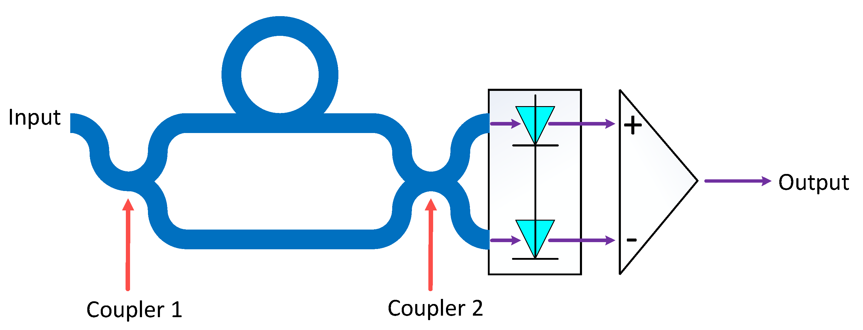
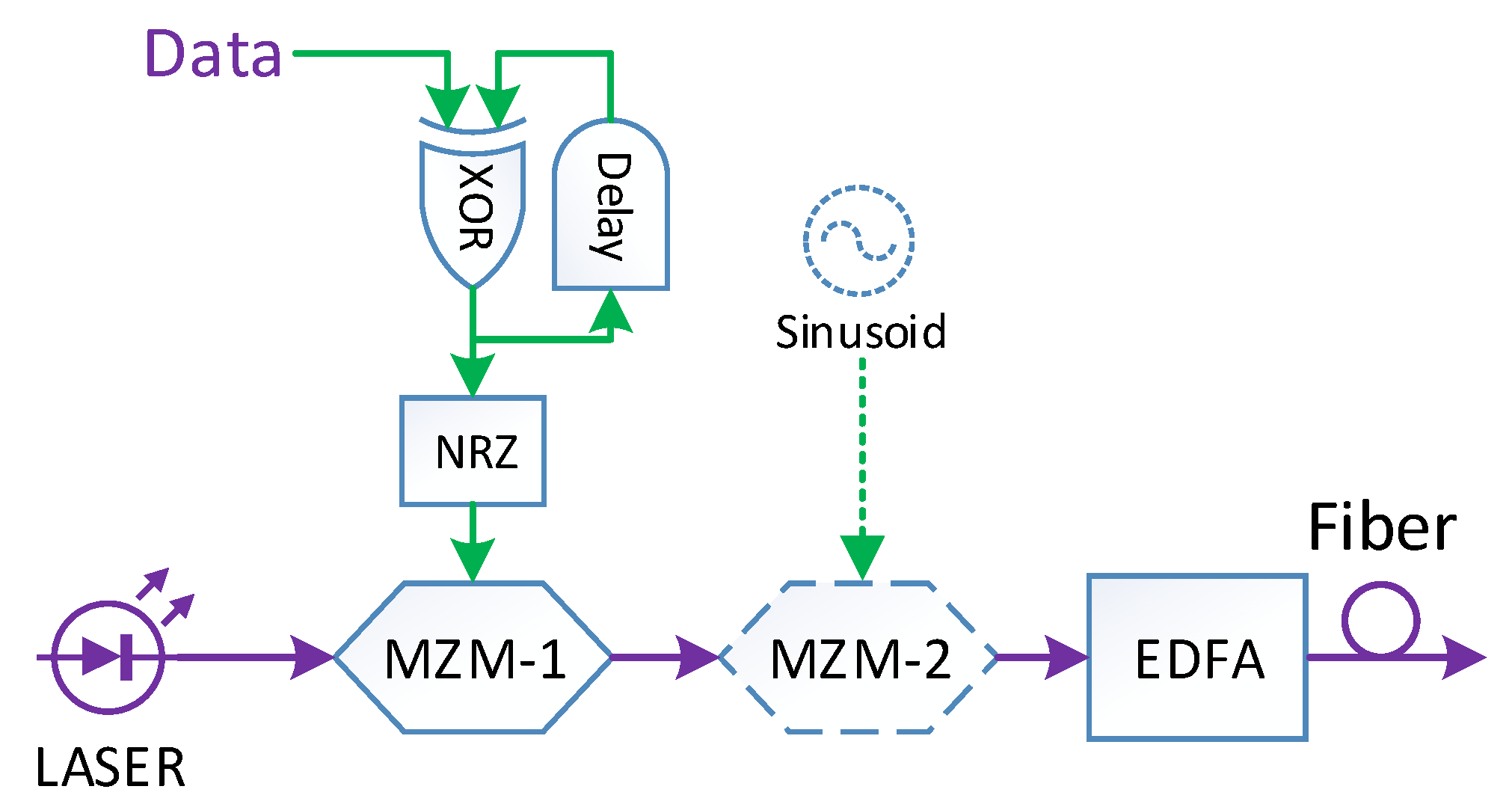
3.1. DPSK Modulation and Balanced Detection

Figure 1 shows a schematic diagram of a DPSK modulation process based on Mach–Zehnder modulators (MZM), which are most widely used in DPSK transmission systems.
The optical electric field of the laser is represented as E i n = | E 0 | exp ( j ω c t ) , where ω c denotes the frequency of the optical carrier emitted by the laser. Two MZMs are applied to achieve return-to-zeros (RZ) or non-return-to-zero (NRZ) DPSK modulations. The first MZM (represented as MZM-1 in Figure 1) generates a phase-shift that is controlled by the pre-encoded data bits. For NRZ-DPSK formats, the second MZM (represented as MZM-2 in Figure 1) is not required. In RZ-DPSK transmission systems, the second MZM is used as an additional modulator, called a pulse carver [25], to implement RZ transmitters by carving out pulses from an NRZ signal. The sinusoid component in Figure 1 is implemented to generate the RZ signals, and the frequency of the sinusoid is half of the frequency of the NRZ signal.
MZMs work by means of the principle of interference. An MZM consists of an input Y-branch waveguide, two phase-modulated arms with independent drive electrodes, and an output Y-branch waveguide [26,27]. If we ignore the machining error and nonlinear effects of the MZM, the optical field transfer function of the MZM can be simply represented as follows:
T = cos [ π 2 V π ( V 1 V 2 ) ] e j π 2 V π ( V 1 + V 2 ) ,
where V1 and V2 are the control voltage of the two phase modulated arms, respectively, V π is the voltage that is required to change the phase in one modulator arm by π and thereby lets the MZM switch from full transmission to full extinction. V π is a constant corresponding to each MZM, and V1 and V2 are used to control the MZM to achieve amplitude or phase modulations. In practice, Equation (1) is always written as follows [26]:
T = cos [ π 2 V π ( V d V b i a s ) ] e j π 2 V π V b i a s .
where V b i a s = V 1 + V 2 is denoted as the bias voltage of the MZM, and V d = 2 V 1 is called the driver voltage of the MZM.
At the first MZM, we let the bias voltage V b i a s = V π , and V d is controlled by the pre-encoded NRZ data. The output optical field transfer function of the first MZM is represented as follows:
E 1 = E i n T = | E 0 | e j ω c t cos [ π 2 V π ( a ( t ) V π ) ] e j π 2 = { j | E 0 | e j ω c t , a ( t ) = V π j | E 0 | e j ω c t , a ( t ) = 3 V π ,
where a(t) denotes the voltage controlled by the pre-encoded NRZ data corresponding to the bit stream to be transmitted, a ( t ) = V π represents the information “0” to be transmitted, and a ( t ) = 3 V π represents the information “1” to be transmitted.
Equation (3) can be written as follows:
E 1 = { | E 0 | e j ( ω c t + π / 2 ) , a ( t ) = V π | E 0 | e j ( ω c t + 3 π / 2 ) , a ( t ) = 3 V π .
Different NRZ signal amplitudes cause the phase shift on the original optical wave from the laser, and the phase difference between information “0” and information “1” is π . Therefore, the amplitude of the pre-encoded NRZ signal is transferred to the differential phase-modulated signal.
RZ-DPSK-modulated signals have better performance than NRZ-DPSK signals [28], so the second MZM is always needed to carve out pulses from an NRZ signal to achieve RZ-DPSK modulation in most practical transmission systems. There are several different carving methods, such as 33% RZ-DPSK, 66% RZ-DPSK, and CSRZ-DPSK. Here, we take the 33% RZ-DPSK as an example to briefly show the RZ carving procedure. The other carving methods are described in detail in plenty of other references [2,25,28,29].
At the second MZM, which works on 33% RZ-DPSK, the bias voltage V b i a s = V π , and the driver voltage is a sinusoidal signal with a frequency of half that of the NRZ signal clock. As such, the output of the second MZM is
E 2 = E 1 cos [ π 2 V π V π sin ( π f t ) ] = ± j | E 0 | cos [ π 2 sin ( π f t ) ] e j ω c t ,
where f is the frequency of the NRZ signal.
After modulation, the optical signal is transmitted via an erbium-doped optical fiber amplifier (EDFA).
Figure 2 shows a balanced demodulation process based on a DLI. It consists of two fiber couplers. The input optical signal is split into two parts in the coupler. A portion of the received signal has a delayed one-bit-length and is reinserted into the signal path in the second coupler. Therefore, the signal interferes with a delayed version of itself upon detection to produce a constructive interference if the phase difference between the two interfering portions of the signal is zero and destructive interference if it is π .
According to coupling theories [30], the output optical field of the DLI can be represented as follows:
{ E o u t 1 = [ e j Δ ϕ ρ 1 ρ 2 ( 1 ρ 1 ) ( 1 ρ 2 ) ] E r E o u t 2 = [ j ( 1 ρ 1 ) ρ 2 + j e j Δ ϕ ρ 1 ( 1 ρ 2 ) ] E r ,
where Eout1 and Eout2 denote the first output and the second output of the DLI, respectively, Er denotes the received optical signal, Δ ϕ is the phase difference of the two waveguide paths, and ρ 1 and ρ 2 are the proportions of them, respectively. The ideal proportion configuration is 50–50%; hence, ρ 1 = ρ 2 = 0 . 5 . If we ignore the machining error of the DLI, Equation (6) can be simplified as follows:
{ E o u t 1 = 1 2 [ e j Δ ϕ 1 ] E r E o u t 2 = j 2 ( 1 + e j Δ ϕ ) E r .
We assume that chrome dispersion is compensated and can ignore the nonlinear effects on the transmission fibers, so the optical field of the received signal can be simply represented as follows:
{ E r = α E 1 , NRZ-DPSK E r = α E 2 , 33 %   RZ-DPSK ,
where α is a linear attenuation coefficient of the transmission, and E1 and E2 are the output of the NRZ-DPSK- and RZ-DPSK-modulated signals represented in Equations (4) and (5), respectively. Therefore, we have the outputs of a DLI represented in Equation (7), which can be calculated as follows:
{ E o u t 1 = 1 2 ( e j Δ ϕ 1 ) α E 1 = ± j α | E 0 | 2 ( e j Δ ϕ 1 ) e j ω c t NRZ-DPSK E o u t 2 = j 2 ( 1 + e j Δ ϕ ) α E 2 = ± j α | E 0 | 2 ( e j Δ ϕ 1 ) cos [ π 2 sin ( π f t ) ] e j ω c t 33 %   RZ-DPSK .
The function of DLI is a phase-to-intensity conversion at the receiver. Therefore, the balanced detector shown in Figure 2 detects the differential power between the two output signals of the DLI. According to Equation (9), the power of the two DLI outputs and the differential power Δ P are calculated as follows:
(1) The NRZ-DPSK case:
P o u t 1 = | E o u t 1 | 2 = 1 2 [ 1 cos ( Δ ϕ ) ] α 2 | E 0 | 2 ,
P out 2 = | E o u t 2 | 2 = = 1 2 [ 1 + cos ( Δ ϕ ) ] α 2 | E 0 | 2 ,
Δ P = P 1 P 2 = cos ( Δ ϕ ) α 2 | E 0 | 2 ,
(2) The 33% RZ-DPSK case:
P o u t 1 = | E o u t 1 | 2 = 1 2 cos 2 [ π 2 sin ( ω t 2 ) ] [ 1 cos ( Δ ϕ ) ] α 2 | E 0 | 2 ,
P out 2 = | E o u t 2 | 2 = = 1 2 cos 2 [ π 2 sin ( π f t ) ] [ 1 + cos ( Δ ϕ ) ] α 2 | E 0 | 2 ,
Δ P = P 1 P 2 = cos ( Δ ϕ ) cos 2 [ π 2 sin ( π f t ) ] α 2 | E 0 | 2 .
In the ideal case, Δ ϕ equals 0 when pre-encoded NRZ data “0” is transmitted and π when pre-encoded NRZ data “1” is transmitted. In this case, the differential power Δ P has the maximum distance between the “0” code and the “1” code to distinguish the differential phase of the delayed and non-delayed optical signals in DLI. However, Δ ϕ may not equal the integer multiplied by π . In this case, the possible value of cos ( Δ ϕ ) becomes η or 1 η ( η > 0 ) , and therefore, the distance of Δ P between the “0” and “1” code is reduced. This fact may cause bit errors to increase at the receiver.
Δ ϕ is represented as follows:
Δ ϕ = 2 π n Δ L / λ ,
where n is the effective refractive index of the fiber in a DLI, Δ L is the differential length of then two paths, and λ is the wavelength of the received optical signal. Equation (16) shows that Δ ϕ is determined by the delay length in the DLI and the wavelength (or carrier frequency) of the light emitted from the laser at the transmitter shown in Figure 1. Therefore, DLI devices should be able to be adjusted to reduce the influences of machining errors and adaptively match the received wavelength.

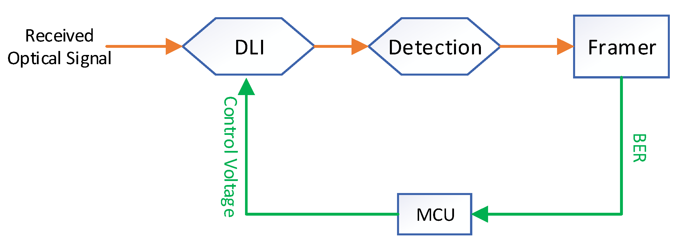
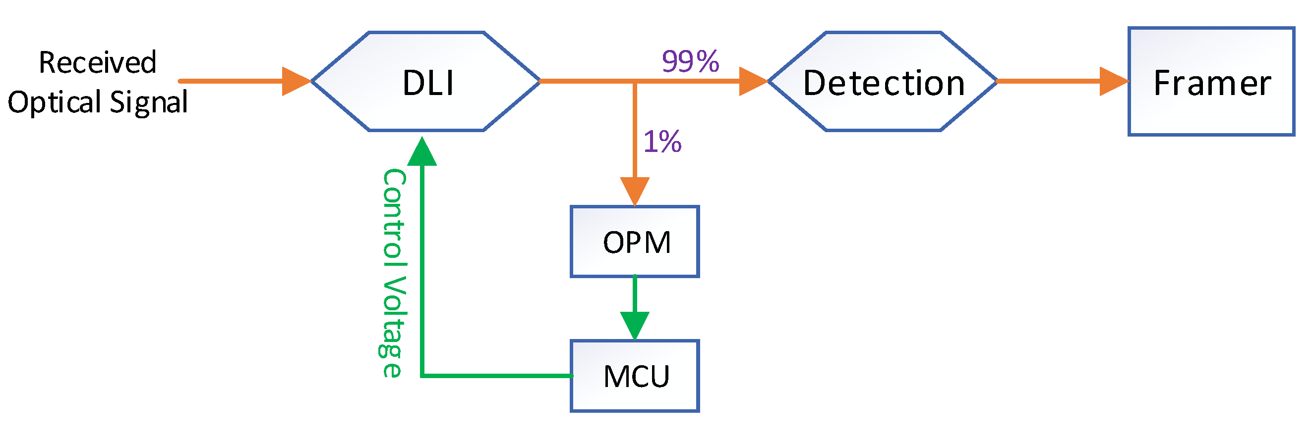
3.2. Phase-Shift Control of DLI

The phase-shift is controlled by adjusting the delay length of one of the paths in DLI. Many methods and corresponding commercial products can be applied to convert voltage signals to the delay length. Therefore, we can adjust the control voltage of a DLI to achieve the phase-shift.
However, the exact control voltage is always unknown because of the following facts:
(1) The wavelength of the received optical signal is uncertain. For different wavelengths, we must adopt different delay lengths so that Δ ϕ equals integer multiples of 2 π at constructive interference. If the received optical signal is unknown or changeable, the receiver must adaptively adjust the delay length to match the received optical signal.
(2) The machining errors affect the actual delay length of the DLI. Because of the machining errors, each individual DLI device has s different delay length compared to other individual DLI devices at the same control voltage.
(3) The machining errors and control errors of the modulator at the transmitter affects the delay length that is actually required.
(4) Residual dispersion, nonlinear effects, and other signal issues that occur during transmission [31] affect the delay length that is actually required.
Therefore, a dynamic adjustment scheme must be implemented in DPSK demodulations. Traditional methods usually scan the whole range of the control voltage and locate the optimum position that maximizes the output optical power of the DLI [8]. This method adopts a splitter to divide the output of the DLI into two parts. The main part is sent to the balanced detector to generate the electrical signal, and another part, which is only in small amounts, is sent to an optical power meter (OPM). A microprogrammed control unit (MCU) scans the whole range of the control voltage, records the optical power reed using the OPM on each step, and finally allows the DLI to work at the voltage that the OPM reading is at its maximum. The scheme is shown in Figure 3. Reference [18] presents a method that can be used to search the local optimum position, which indeed reduces the searching time. However, the proposed method in [18] still requires the scanning part of the control voltage range and the optical output power of the DLI that only indirectly reflects the demodulation quality. Another disadvantage of using the optical output power of the DLI as the feedback of the DLI control is that when the received signal is changed or deteriorated, finding MCU is usually difficult, as is re-adjusting the DLI.
In this paper, we consider the application of artificial intelligence algorithms as an effective method to observably reduce the search time and adopt the bit-error-rate (BER), which directly reflects the demodulation quality as the feedback to adjust the DLI. The improved dynamic DLI control voltage resolving scheme is shown in Figure 4. If the Framer is designed based on FPGA, the MCU can be removed, and the DLI control voltage is controlled by the FPGA directly. We only need to test a few points of the DLI control voltage to predict the optimal value based on the FNN. The proposed method does not require the MCU to scan the whole range of the DLI control voltage, so the searching time can be observably reduced. The details of the proposed algorithm are described in the following section.

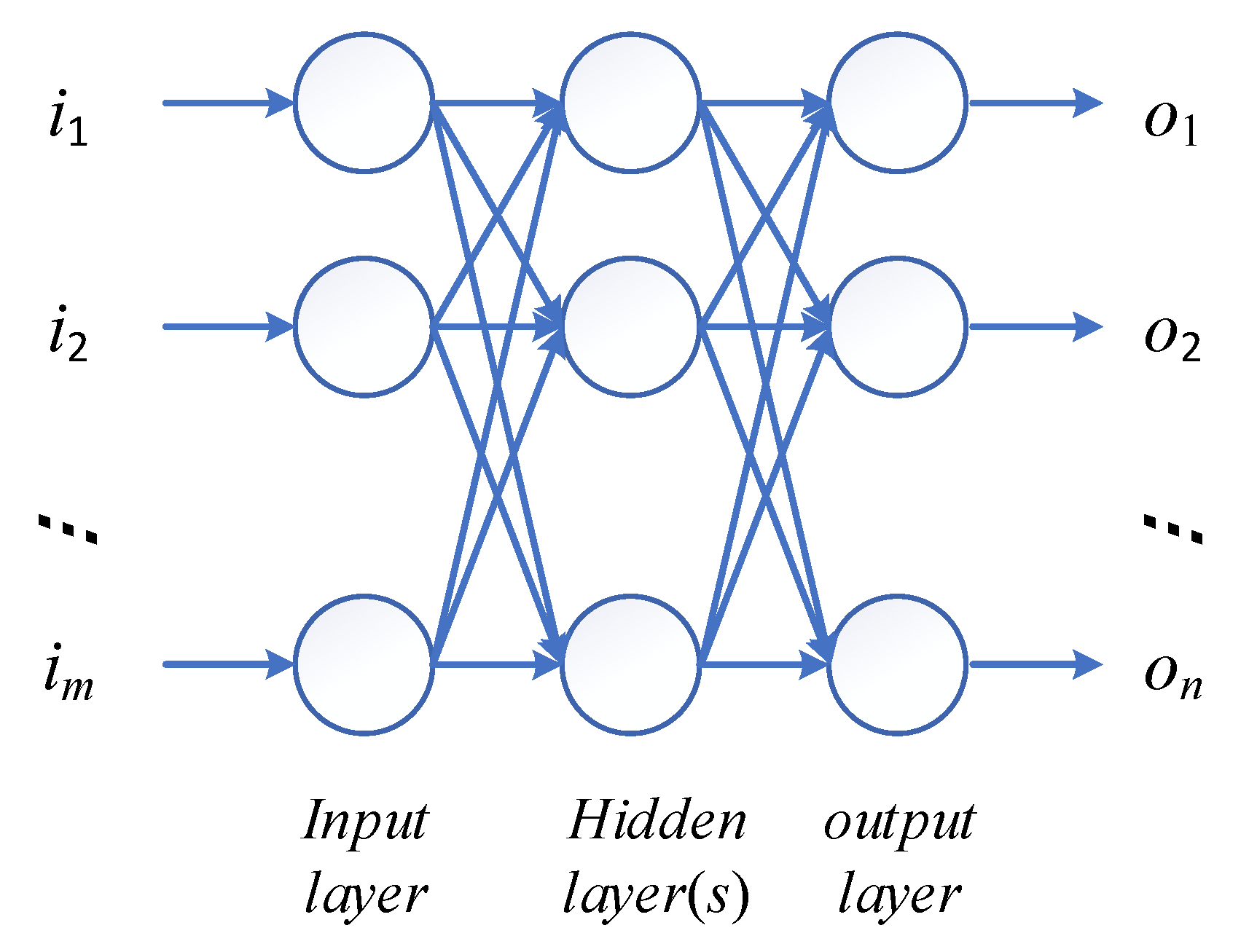
4. Optimal DLI Control Voltage Resolving Based on FNN

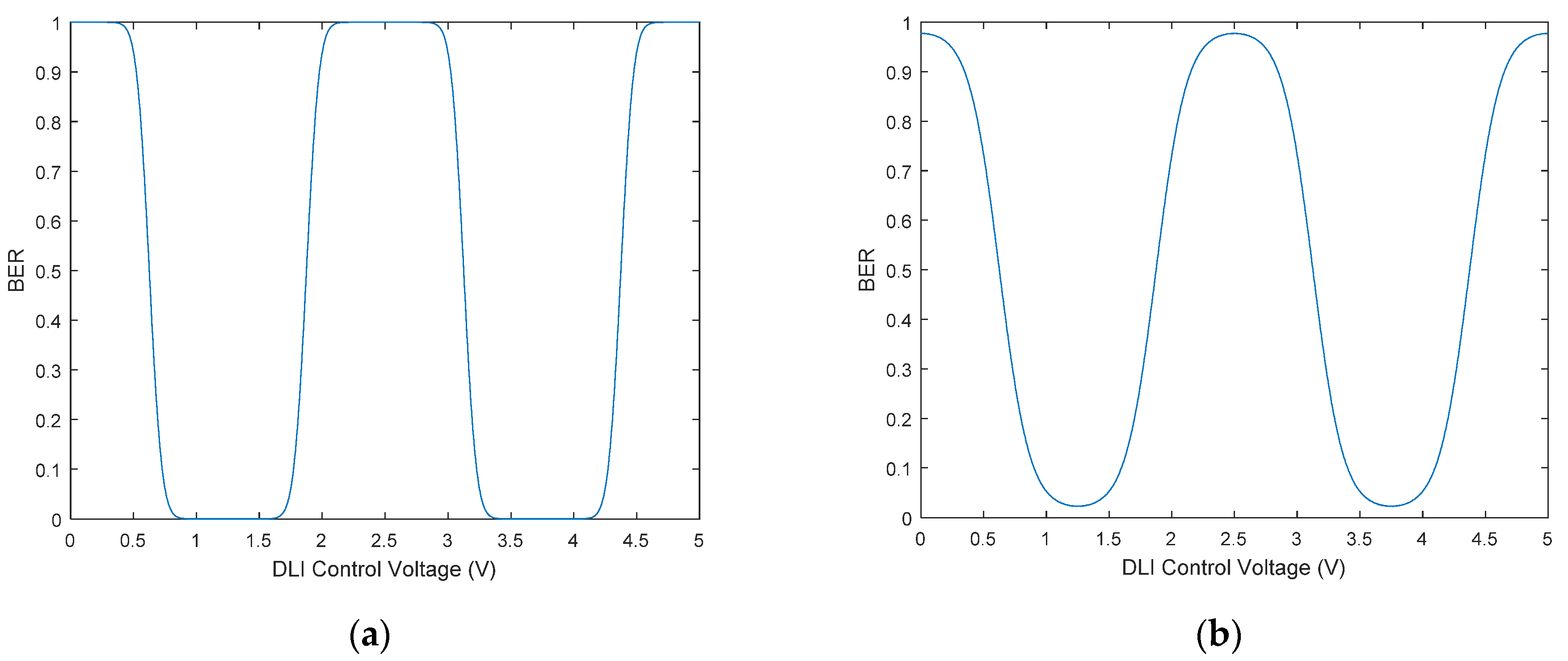
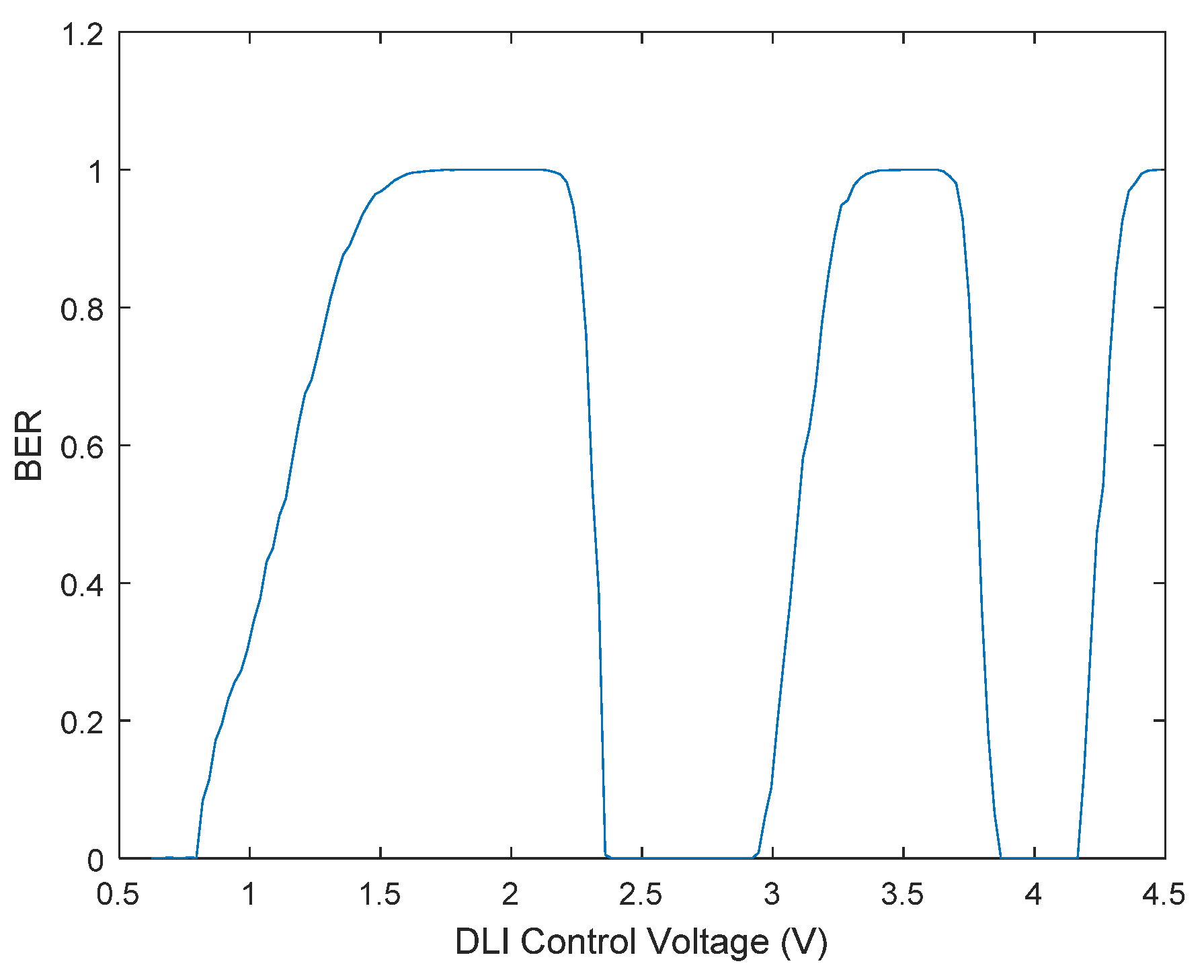
4.1. Feasibility Analysis

As shown in Equations (10)–(15), the demodulation performance is mainly affected by cos ( Δ ϕ ) , which is a continuous function of Δ ϕ . Δ ϕ is approximately linear to the control voltage of the DLI. For the reasons described in Section 3.2, the exact control voltage for different wavelengths and different individual DLI devices is difficult to resolve, especially when the wavelength of the received optical signal is changing.
An FNN has simple structures and wide applications and can approximate any continuous function and can square integrable functions with arbitrary precision. A feedforward network is a kind of static nonlinear mapping, and its complex nonlinear processing ability can be obtained through the compound mapping of simple nonlinear processing units. Therefore, an FNN has demonstrated good performance in solving nonlinear problems that are difficult to model using traditional methods.
If we ignore the nonlinearity between the control voltage and the delay length of the DLI device, we can simulate and draw the BER curve of the received signal while the DLI control voltage increases, as shown in Figure 5. Figure 5a represents cases with a high optical signal to noise ratio (OSNR), and Figure 5b represents the cases with a low OSNR. Theoretical analysis and simulation results both denote that the relationship between the BER and DLI control voltage is nonlinear and continuous. As such, the FNN is suitable to resolve the best control voltage.
Figure 6 shows a practical collected BER curve when the DLI control voltage increases. If we compare it with the simulated curves in Figure 5, we can see that the practical curve is not totally repeated periodically. This phenomenon is caused by the nonlinearity of the DLI devices. Unfortunately, the nonlinear phenomenon is determined by the product process and is different for each individual. Therefore, the best DLI control voltage is difficult to resolve using traditional methods, with the exception of scanning the whole range of the DLI control voltage. However, an FNN can be trained to match the relationship between the BER and the DLI control voltage, and it can then be used to predict the optimal control voltage that minimizes the BER based on very low testing points. This method avoids scanning the whole range of the DLI control voltage, so the elapsed time can be significantly reduced.

4.2. Algorithm Model

The structure of an FNN is shown in Figure 7. It usually consists of one input layer, one output layer, and several hidden layers [32]. The hidden layers can be trained to approximate the linear, nonlinear, or continuous functions.
In this paper, we consider using an FNN to match the relationship between the DLI control voltage and the BER. Based on the theoretical analysis in Section 3.1, the biggest primary factor that influences the demodulation performance is a cosine function, so we propose setting the parameters of the FNN as follows:
(1) Input Layer Nodes:
We propose using three positions in a single descending part of the BER curve to predict the minimal BER followed by the previously referred to descending curve section, so we set up the input layer to constitute three nodes. The input values of the three inputs are the three tested BER results corresponding to the selected control voltage values. The differences among the selected control voltage values are equal.
(2) Structure of the Output Layer:
The purpose of the proposed method is to predict the minimal BER and to resolve the corresponding DLI control voltage, so we set the output be the differential voltage between the mean voltage of the three input nodes and the expected control voltage.
(3) Structure of the Hidden Layers:
The settings of the hidden layers of a neural network are usually unexplainable, so the accurate theoretical analysis of an FNN is difficult. We set the number of nodes in the hidden layer according to the experiments and simulation experiments. According to the literature [33], when the number of nodes in the hidden layer is between the number of nodes in the input layer and the number of nodes in the output layer, and especially when it is closer to the number of nodes in the input layer, the network convergence speed is faster. When the number of hidden nodes is too small, the learning process does not converge. However, when there are too many nodes in the hidden layer, the training of the network is easy to overfit, and the training results are seriously affected by noise. The number of the input layer nodes is three, and the number of the output layer nodes is one, so the optimal number of the nodes in the hidden layer should be between one and three if we adopt the idea proposed in [33].
We also studied the training performance achieved by computer simulations based on the Levenberg–Marquardt training method when the number of the hidden layers is increased from one to five. Performance is denoted by the average training time and mean squared error. The simulation results are shown in Table 1. When the number of hidden nodes is three, the training performance is relatively superior. Therefore, we set the number of the nodes in hidden layer to be three.

4.3. Tranning the FNN

In this section, we propose the following procedure to train the FNN described in Section 4.2.
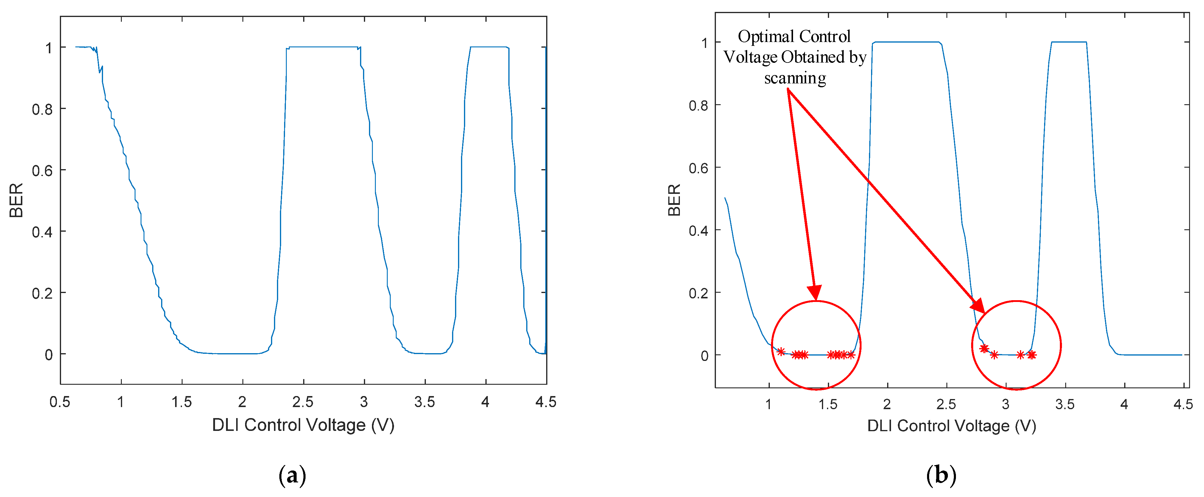
  • Scan the whole range of the DLI control voltage and obtain the BER values on all of the test points. The control voltage values and the corresponding BER values are represented by the vector v and e, respectively.
  • Select the data in v and e to construct the training sets X and Y, respectively, and follow the rules below:
(1) X consists of some vectors, each of which has three elements. We represent X as follows:
X = [ x 11 x 12 x 13 x 21 x 22 x 23 x n 1 x n 2 x n 3 ] .
(2) The three elements of each line in X are increasing and have the same interval as shown in Equation (18). For most commercial DLI devices, 100 mV is a generally suitable interval value.
x i 3 x i 2 = x i 2 x i 1 = 100 mV ,   1 i n .
(3) Y consists of the BER values corresponding to the control voltage values collected in X and defined in Equation (17).
Y = [ y 11 y 12 y 13 y 21 y 22 y 23 y n 1 y n 2 y n 3 ] .
(4) The three elements of each line in Y are descending, i.e.,
y i 3 < y i 2 < y i 1 ,   1 i n .
Equations (18) and (20) should both be satisfied. Otherwise, the vector pair should be removed from X and Y.
3.
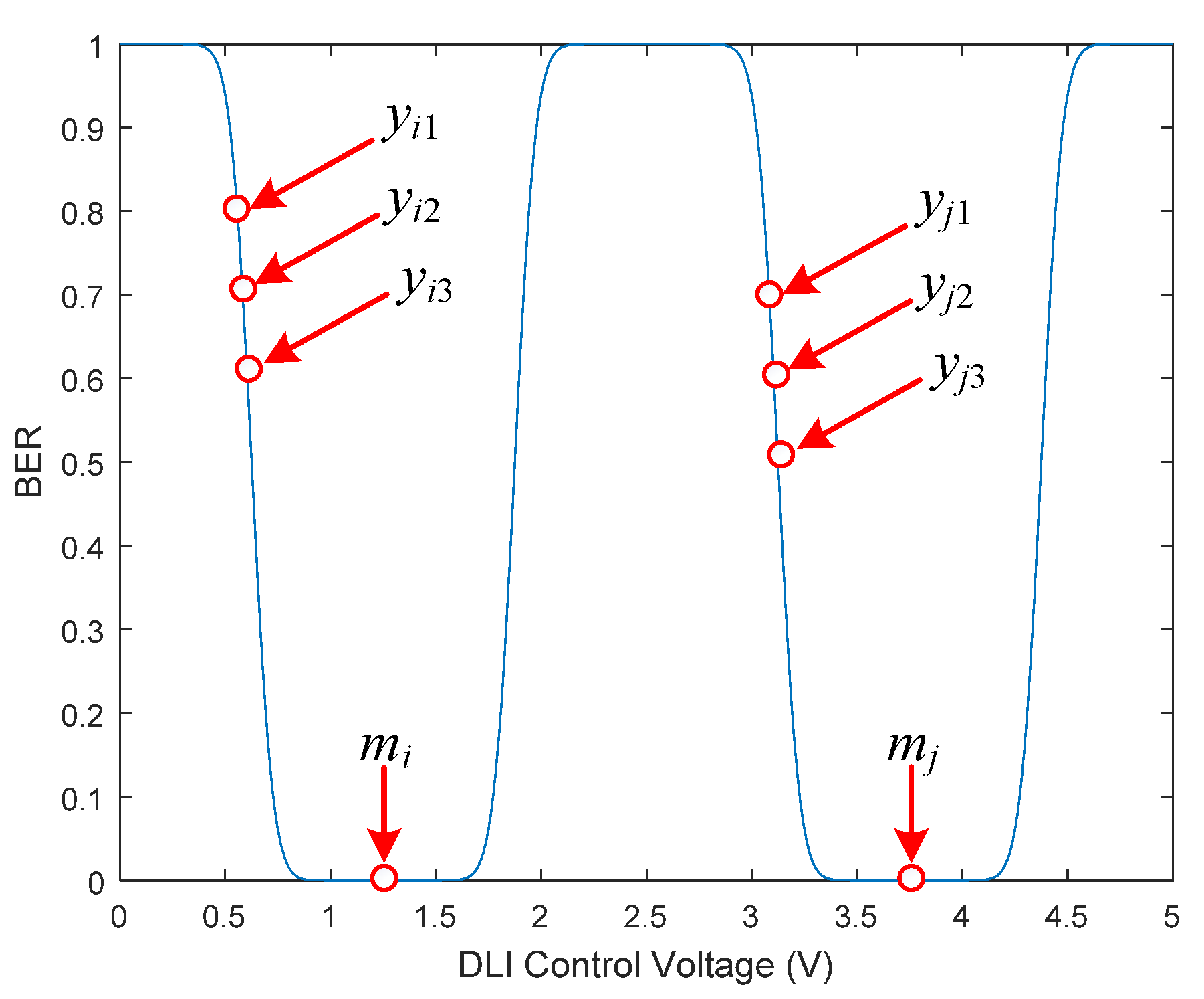
Mark the local minimum values in y nearest to each row in Y, as shown in Figure 8. The marked values consist of a vector, which is represented by M as follows:
M = [ m 1 m 2 m n ] .
4.
Make the target vector T according to the marked points as follows:
T = [ Δ v 1 Δ v 2 Δ v n ] ,
where
Δ v i = x m i x i 2 , 1 i n ,
where x m i denotes the control voltage corresponding to the marked BER value m i .
5.
Train the FNN described in Section 3.2 based on matrix Y and vector T, where each row in Y is an input vector and the corresponding element in T is the respective target. The training data pairs are also shown in Table 2.

4.4. Implementaion of the Trained FNN

After training, the FNN can be applied to quickly predict the optimal control voltage by searching and testing very low points. The proposed procedure can be described as follows:
1.
Set a starting control voltage to start a searching procedure. Most commercial DLI devices have better linearity and performance in the middle part of the whole control voltage range, so we suggest setting the starting position at 1/4 of the maximum control voltage. For example, if the control voltage of a DLI is 0 to 5 V, we can set the starting position at about 1.2 to 1.5 V.
2.
Scan the DLI control voltage with the fixed interval, which is set the same as it was in the training procedure. For most commercial DLI devices, 100 mV is a generally suitable interval value.
3.
Test the BER at each control voltage while scanning. If three continuous tested BER values are descending, we use the corresponding three control voltage values (represented by the vector [ v 1 v 2 v 3 ] ) as the inputs of the FNN and obtain the output (represented by Δ v ).
4.
Let v = v 2 + Δ v and set the control voltage of the DLI by v .
5.
Check the BER on the control voltage v to judge whether the demodulation performance satisfies the system requirements. If the BER is higher than the threshold, we make minor adjustments to the control voltage near v to revise the predicted value.

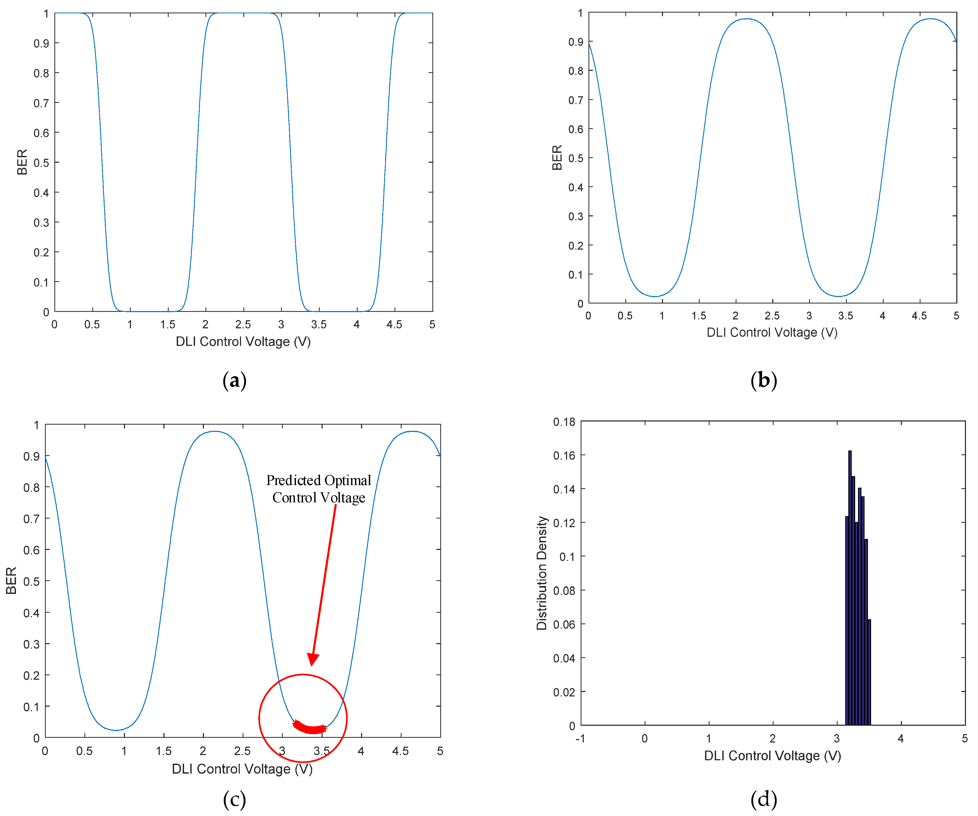
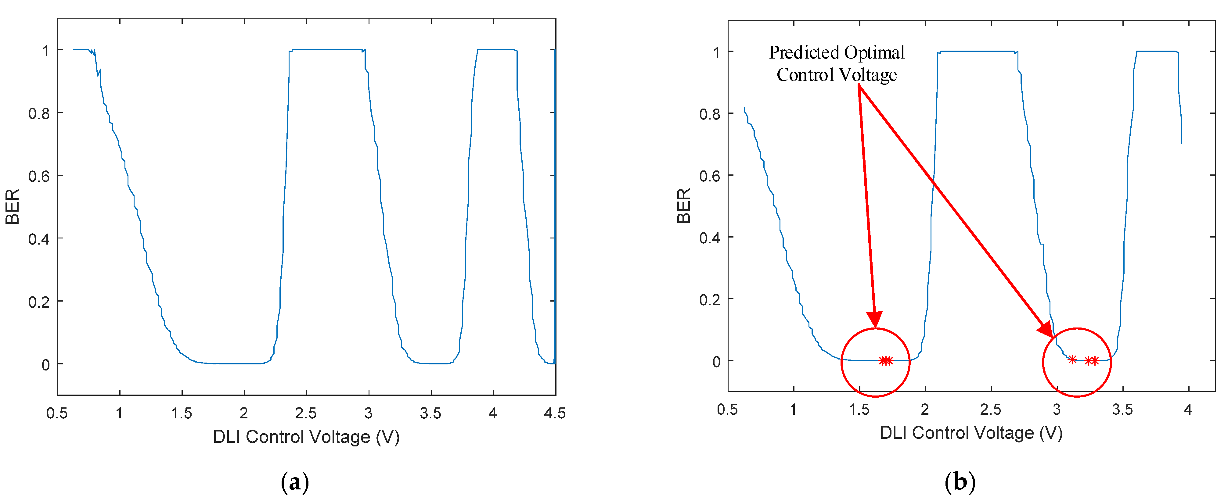
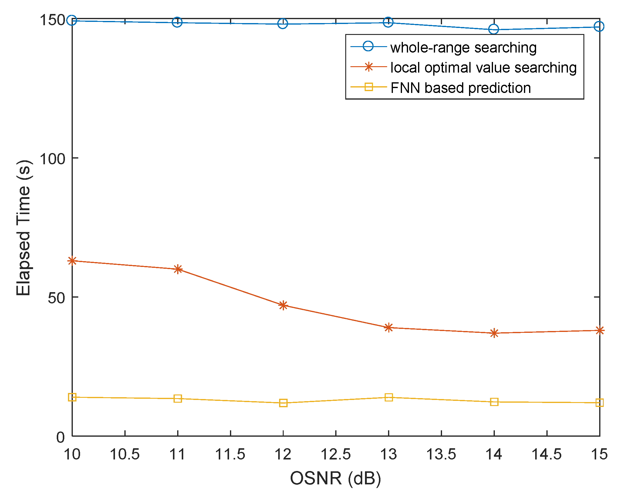
5. Simulation and Implementation

5.1. Simulation Results

In this section, we present some simulation experiments to show the efficiency of the method proposed in this paper.
First, we prepared the data to train the FNN. We assume that the whole range of the DLI control voltage to be 0 to 5 V and that the fiber transmission channel is a binary symmetric channel. The data are generated by following the steps below:
Step 1. Generate a random data sequence that consists of 100,000 bits.
Step 2. Modulate the generated sequence according to Figure 1 and transmit it in a noisy fiber channel. We used the binary symmetric and additive white gaussian noise channel model to simplify the transmission model.
Step 3. Let the DLI control voltage increase from 0 V to 5 V with an interval 0.005 V for each step. We assume that the base phase shift ϕ 0 at 0 V is π . We demodulate the received optical signal and calculate the BER at each step. This procedure generates the vectors v and e, which were defined in Section 4.3.
Step 4. Construct the FNN algorithm model described in Section 3.1 and generate the training data X and T defined in Section 4.3 based on the vectors v and e.
Second, we trained the FNN algorithm model following the steps given in Section 4.3.
Finally, we generated new data sets to test the trained FNN and validate the efficiency of the proposed method. The test data are generated by following the steps below:
Step 1. Randomly shift the base phase by Δ ϕ and change the noise level and re-generate the vectors v and e, which were defined in Section 4.3. The generation procedure is similar to method used to prepare the training data that was described above.
Step 2. Randomly set a start control voltage value and obtain three test points with the interval 100 mV. If the corresponding BER values, which are obtained by searching the vector e, at such three test points are descending, implement the trained FNN to calculate the offset voltage Δ v and set the predicted minimal control voltage to the DLI. The detailed process is listed in Section 4.4.
Step3. Make minor adjustments to the control voltage near the predicted value if necessary.
In Step 1, the purpose of randomly shifting the base phase by Δ ϕ is to simulate the algorithm performance on the different wavelengths of the received optical system because the phase shift is different when the wavelength is changed, as shown in Equation (16). Additionally, we set a different noise level to check the adaptability of the proposed method in different transmission conditions.
Figure 9 shows the simulation results of when we executed the simulation steps described above. Figure 9a shows the BER curve of the training data sets when the DLI control voltage increases from 0 V to 5 V. The base phase shift, i.e., the phase shift occurring when the control voltage equals 0, is set as π . We trained the FNN algorithm model based on this data set.
After training, we generated the test data set and drew the BER curve in Figure 9b. It is shown that the base shift changed and that the noise is enhanced. We randomly selected a voltage value to start a searching procedure and predicted the optimal DLI control voltage to demodulate the received optical signal base on the method proposed in Section 3. We tested the model 10,000 times and marked the predicted optimal DLI control voltage with “*”, as shown in Figure 9c. It is easy to see that the predicted voltage values converge well and are distributed near the real optimal value. We also draw the distribution density of the predicted voltage values, as shown in Figure 9d.
The results show that the proposed method can predict the optimal DLI control voltage to minimize the BER even though the noise level and base phase shift are different from the training data sets, which is equivalent to the changes that occur in the wavelength and transmission conditions in practical telecommunication systems.

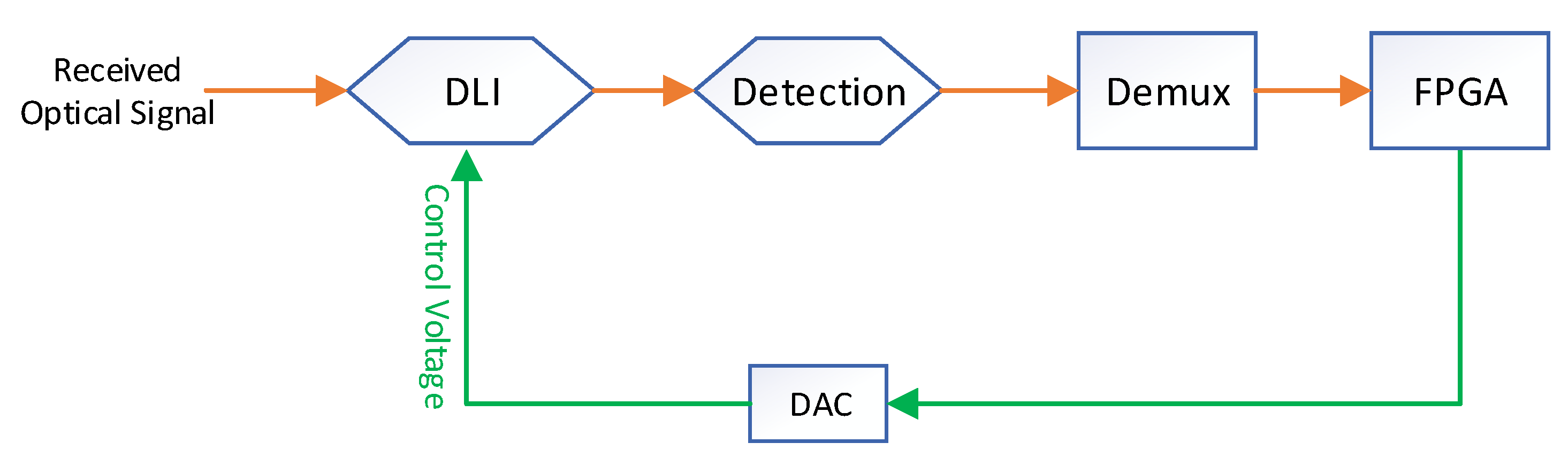
5.2. Implementations on FPGA

In this section, we briefly show an implementation of the proposed method and compare its performance with traditional methods based on search time.
One of our designed DPSK receivers is shown in Figure 10. This receiver was applied in a DWDM transmission system, and the symbol rate was 43 Gbps. An FPGA device was applied to process the received frames. Therefore, the FNN can be implemented in FPGA, and the DLI control voltage can also be controlled by the FPGA.
During training, the receiver analyzes the statistics and collects the BER data by scanning the control voltage. The BER data can be obtained by checking the frame alignment signals (FAS), which are known by the receiver. FAS is a fixed segment in the transmitted stream and appears periodically. Using the statistics of the FAS errors to estimate BER can avoid the need for the transmitter to send training data. Figure 11a shows the BER curve collected by a practical receiver. The measurement error is limited to ± 1 bit per second. For example, if the optical signal has 50,000 frames at each second, the measurement error is limited to ± 1 / 50,000 .
The training process can be implemented using a software on a computer or an embedded operation system in FPGA. Training on a computer is faster and is more flexible to adjust the structure and the parameters of the FNN model.
After training, we can obtain the weight coefficients between the layers of the FNN and can generate a memory file following the format supported by the FPGA development toolkit. Then, we can compile the FPGA program, which is combined with the memory file, and can implement it in the FPGA. The structure of the FNN is designed in the FPGA program based on fixed digital signal process (DSP) units and logical gates, and the trained weight coefficients are read out from a specified memory.
We change the received optical signal to another channel of the DWDM system and start scanning the DLI control voltage from a fixed starting point (1.25 V). We tested the system 1000 times and marked the predicted optimal control voltage values, as shown in Figure 11b.
To compare the performance of the proposed method with traditional scan-based methods, we also ran the scan-based methods proposed in [8,18] and show their performance in Figure 12. Figure 12a represents the BER curve of the test data, and Figure 12b marks the optimal control voltage obtained by scanning. Compared to the method proposed in this paper, the scan-based methods do not converge well.
We also compared the average elapsed time needed to lock to the optimal DLI control voltage based on the different methods shown in Table 3. We compared the performance of the proposed method and the traditional methods [8,18]. The results show that the proposed method can significantly reduce the search time. It resolves the optimal DLI control voltage quickly. Furthermore, we determined the elapsed time needed for the search procedure when the OSNR increased.
As shown in Figure 13, the average elapsed time of the whole-range search method [8] is approximately 150 s for all of the OSNR values. The elapsed time of the local optimal value searching method [18] was reduced when the OSNR increased. However, the average elapsed time was still above 35 s. While applying the FNN-based prediction method, the elapsed time for all of the OSNR values was lower than 15 s.

6. Discussion

In this paper, we presented a problem that prevents the implementation of balanced detection demodulations for DPSK optical transmission systems. DPSK is an advanced modulation method that is widely used in modern optical communications. However, in low-cost, balanced detection-based applications, it is difficult to resolve the phase control rapidly. In our work, we found that the optimal DLI control voltage can be rapidly predicted by several test points based on the FNN. We presented the theoretical analysis and algorithm model of the proposed method in this paper and validated the efficiency of the proposed method using computer simulations and experiments in telecommunication systems.
Through the computer simulations, it was validated that the proposed algorithm can accurately predict the optimal control voltage of a DLI based on just three valid test points by following some specific rules. Furthermore, we implemented the proposed method in FPGA, the core device of a telecommunication system and compared the performance of the proposed method with the performance of the traditional scan-based methods in the literature. The comparison experiments were run in different OSNR conditions. According to the analysis of the experiments, the method proposed in this paper has two major advantages: First, the resolved optimal control voltage converges better than the scan-based methods. Second, the elapsed time needed to locate the optimal control voltage is significantly lower.
The proposed method can be expanded to applications in many of low-cost and short-reach telecommunications that implement phase shift keying-modulated signals. However, further research may improve the performance or extend the applications ulteriorly, for example, the applications in differential quadrature phase shift keying (DQPSK) modulation systems.

7. Conclusions

In this paper, we proposed a new method to quickly locate the optimal DLI control voltage based on an FNN. The simulation results and implementation performance show that the proposed method requires less search time and can correctly predict the optimal DLI control voltage to minimize the BER even though the noise level and wavelength are different from the training data sets. This is an efficient method to optimize the response time for phase shift keying modulated telecommunication systems.

Author Contributions

J.Z. was responsible for the analysis and simulations of the proposed method. D.L. implemented the proposed method in practical telecommunication systems and validated the performance. All authors have read and agreed to the published version of the manuscript.

Funding

This research received no external funding.

Institutional Review Board Statement

Not applicable.

Informed Consent Statement

Not applicable.

Data Availability Statement

Not applicable.

Acknowledgments

This research was supported by the foundation for young scholars of the National University of Defense Technology.

Conflicts of Interest

The authors declare no conflict of interest.

References

  1. Gnauck, A.H.; Liu, X.; Wei, X.; Gill, D.M.; Burrows, E.C. Comparison of modulation formats for 42.7-gb/s single-channel transmission through 1980 km of SSMF. IEEE Photonics Technol. Lett. 2004, 16, 909–911. [Google Scholar] [CrossRef]
  2. Golovchenko, A.E.; Rahman, L.; Bakhshi, B.; Kovsh, D.; Idrovo, F.; Abbott, M. Using RZ DPSK-Based Transponders for Upgrades on Existing Long-Haul Submarine WDM Systems. J. Lightwave Technol. 2008, 26, 204–208. [Google Scholar] [CrossRef]
  3. Dai, Y. Optical Signal Processing of Phase-Modulated Signal for Communication. Ph.D. Thesis, The Chinese University of Hong Kong, Hong Kong, China, 2011. [Google Scholar]
  4. M’Sallem, Y.B.; Park, C.S.; LaRochelle, S.; Rusch, L.A. Multi-Format Wavelength Conversion Using Quantum Dash Mode-Locked Laser Pumps. Photonics 2015, 2, 527–539. [Google Scholar] [CrossRef]
  5. Cai, J.X.; Foursa, D.G.; Liu, L.; Davidson, C.R.; Cai, Y.; Patterson, W.W.; Lucero, A.J.; Bakhshi, B.; Mohs, G.; Corbett, P.C.; et al. RZ-DPSK Field Trial Over 13,100 km of Installed Non-Slope-Matched Submarine Fibers. J. Lightwave Technol. 2005, 23, 95–103. [Google Scholar]
  6. Wang, J. Performance Evaluation of DPSK Optical Fiber Communication Systems. Ph.D. Thesis, University of California, Berkeley, CA, USA, 2004. [Google Scholar]
  7. Zhang, S. Control of A Nonlinear Mach-Zehnder Interferometer for Optical Regeneration Using Digital Signal Processing. Ph.D. Thesis, Queen’s University, Kingston, ON, Canada, 2014. [Google Scholar]
  8. Lu, J. Research on High Speed Laser Communication Experiment System Based on DPSK/Self-Homodying Detection. Master’s Thesis, Harbin Institute of Technology, Harbin, China, 2018. [Google Scholar]
  9. Sudheer, V.R.; Seena, R.; Sankararaman, S. DPSK Based Low Cost Radio Fiber System for Communication. Opt. Quantum Electron. 2019, 51, 150. [Google Scholar] [CrossRef]
  10. Zhang, S.; Cartledge, C. A DSP-Based Control Method for a Nonlinear Mach–Zehnder Interferometer DPSK Regenerator. J. Lightwave Technol. 2015, 33, 3788–3795. [Google Scholar] [CrossRef]
  11. Xu, T.; Jacobsen, G.; Popov, S.; Li, J.; Liu, T.; Zhang, Y.; Bayvel, P. Analytical Investigations on Carrier Phase Recovery in Dispersion-Unmanaged n-PSK Coherent Optical Communication Systems. Photonics 2016, 3, 51. [Google Scholar] [CrossRef] [Green Version]
  12. Rodrigo Navarro, J.; Kakkar, A.; Pang, X.; Iglesias Olmedo, M.; Ozolins, O.; Da Ros, F.; Piels, M.; Schatz, R.; Zibar, D.; Jacobsen, G.; et al. Two-Stage n-PSK Partitioning Carrier Phase Recovery Scheme for Circular mQAM Coherent Optical Systems. Photonics 2016, 3, 37. [Google Scholar] [CrossRef] [Green Version]
  13. Wang, Y. Research on DPSK Demodulation Technology in Coherent Optical Communication System. Master’s Thesis, Xi’an University of Technology, Xi’an, China, 2019. [Google Scholar]
  14. Bayvel, P.; Behrens, C.; Millar, D.S. Digital Signal Processing (DSP) and Its Application in Optical Communication Systems. In Optical Fiber Telecommunications, 6th ed.; Kaminow, I.P., Li, T., Willner, A.E., Eds.; Academic Press of Elsevier: Oxford, UK, 2013; pp. 163–219. [Google Scholar]
  15. Kong, M.; Li, X.; Zhang, J.; Wang, K.; Xin, X.; Zhao, F.; Yu, J. High Spectral Efficiency 400 Gb/s Transmission by Different Modulation Formats and Advanced DSP. J. Lightwave Technol. 2019, 37, 5317–5325. [Google Scholar] [CrossRef]
  16. Buchali, F.; Aref, V.; Dischler, R.; Chagnon, M.; Schuh, K.; Hettrich, H.; Bielik, A.; Altenhain, L.; Guntermann, M.; Schimid, R.; et al. 128 GSa/s SiGe DAC Implementation Enabling 1.52 Tb/s Single Carrier Transmission. J. Lightwave Technol. 2021, 39, 763–770. [Google Scholar] [CrossRef]
  17. Recommendation ITU-T G.694.1: Spectral Grids for WDM applications: DWDM Frequency Grid. 3.0 ed. Available online: http://handle.itu.int/11.1002/1000/14498-en (accessed on 19 July 2021).
  18. Zhou, J.; Huang, Z.; Liu, C.; Su, S. Design of Adaptive Dispersion Compensation and Demodulation System for 40 Gbps RZ-DQPSK Optical Fiber Communication Receivers. Optik 2014, 2015, 370–373. [Google Scholar] [CrossRef]
  19. Xu, Z.; Sun, C.; Ji, T.; Manton, J.H. Feedforward and Recurrent Neural Network-Based Transfer Learning for Nonlinear Equalization in Short-Reach Optical Links. J. Lightwave Technol. 2021, 39, 475–480. [Google Scholar] [CrossRef]
  20. Xu, Z.; Sun, C.; Manton, J.H.; Schieh, W. Joint Equalization of Linear and Nonlinear Impairments for PAM4 Short-Reach Direct Detection Systems. IEEE Photonics Technol. Lett. 2021, 33, 425–428. [Google Scholar] [CrossRef]
  21. He, Y.; Liu, J.; Wang, P.; Xiong, W.; Wu, Y.; Zhou, X.; Cheng, Y.; Gao, Y.; Li, Y.; Chen, S.; et al. Detecting Orbital Angular Momentum Modes of Vortex Beams Using Feed-Forward Neural Network. J. Lightwave Technol. 2019, 37, 5848–5855. [Google Scholar] [CrossRef]
  22. Liang, Y.; Jiang, J.; Chen, Y.; Zhu, R.; Lu, C.; Wang, Z. Optimized Feedforward Neural Network Training for Efficient Brillouin Frequency Shift Retrieval in Fiber. IEEE Access 2019, 7, 68034–68042. [Google Scholar] [CrossRef]
  23. Li, S.; Zhou, J.; Huang, Z.; Sun, X. Modulation Format Identification Based on an Improved RBF Neural Network Trained With Asynchronous Amplitude Histogram. IEEE Access 2020, 8, 59524–59532. [Google Scholar] [CrossRef]
  24. Shen, F.; Zhou, J.; Huang, Z.; Li, L. Going Deeper into OSNR Estimation with CNN. Photonics 2021, 8, 402. [Google Scholar] [CrossRef]
  25. Winzer, P.J.; Essiambre, R.J. Advanced Optical Modulation Formats. In Optical Fiber Telecommunications V B, 5th ed.; Kaminow, I.P., Li, T., Eds.; Academic Press of Elsevier: Oxford, UK, 2008; pp. 23–93. [Google Scholar]
  26. Conradi, J. Bandwidth-efficient modulation formats for digital fiber transmission systems. In Optical Fiber Telecommunications IV B, 4th ed.; Kaminow, I.P., Li, T., Eds.; Academic Press of Elsevier: Oxford, UK, 2002; pp. 862–901. [Google Scholar]
  27. Fatemeh, S. Investigation of Low-Power Integrated Optical Modulators. Ph.D. Thesis, McGill University, Montreal, QC, Canada, 2018. [Google Scholar]
  28. Cao, H.; Shu, X.; Atai, J.; Gbadebo, A.; Xiong, B.; Fan, T.; Tang, H.; Yang, W.; Yu, Y. Optimally-Designed Single Fiber Bragg Grating Filter Scheme for RZ-OOK/DPSK/DQPSK to NRZ-OOK/DPSK/DQPSK Format Conversion. Optics Express 2014, 22, 30442–30460. [Google Scholar] [CrossRef]
  29. Gnauck, A. 40-Gb/s RZ-Differential Phase Shift Keyed Transmission. In Proceedings of the OFC 2003 Optical Fiber Communications Conference, Atlanta, GA, USA, 28 March 2003; pp. 450–451. [Google Scholar]
  30. Zhu, X.; Yuan, L.; Liu, Z.; Yang, J.; Guan, C. Coupling Theoretical Model Between Single-Core Fiber and Twin-Core Fiber. J. Lightwave Technol. 2009, 27, 5235–5239. [Google Scholar]
  31. Wang, J.; Kahn, J.M. Impact of Chromatic and Polarization-Mode Dispersions on DPSK Systems Using Interferometric Demodulation and Direct Detection. J. Lightwave Technol. 2004, 22, 362–371. [Google Scholar] [CrossRef]
  32. Buduma, N.; Lacascio, N. Fundamentals of Deep Learning, 1st ed.; O’Reilly Media, Inc.: Sebastopol, CA, USA, 2017; pp. 17–38. [Google Scholar]
  33. Ye, B.; Lei, Y. Analysis of Choosing the Number of the Hidden layers and Its Nodes Number in Block Propagation Network. J. Shangqiu Vocat. Tech. Coll. 2004, 6, 52–54. [Google Scholar]
Figure 1. DPSK modulation.
Photonics 08 00428 g001
Figure 2. DLI-based demodulation.
Photonics 08 00428 g002
Figure 3. Dynamic DLI control voltage adjusting.
Photonics 08 00428 g003
Figure 4. Improved dynamic DLI control voltage adjusting.
Photonics 08 00428 g004
Figure 5. Simulated BER curve while DLI control voltage is increasing: (a) represents the cases with a high OSNR; (b) represents the cases with a low OSNR.
Photonics 08 00428 g005
Figure 6. Improved dynamic DLI control voltage adjusting.
Photonics 08 00428 g006
Figure 7. Structure of an FNN.
Photonics 08 00428 g007
Figure 8. Mark the target points.
Photonics 08 00428 g008
Figure 9. Simulation results: (a) represents the BER curve of the training data; (b) represents the BER curve of the test data; (c) marks the predicted optimal control voltage; (d) shows the distribution density of the predicted voltage values.
Photonics 08 00428 g009
Figure 10. A DPSK receiver.
Photonics 08 00428 g010
Figure 11. Implementation performance of the proposed method in FPGA: (a) represents the BER curve of the training data; (b) marks the predicted optimal control voltage.
Photonics 08 00428 g011
Figure 12. Implementation performance of the scan-based method in FPGA: (a) represents the BER curve of the test data; (b) marks the optimal control voltage obtained by scanning.
Photonics 08 00428 g012
Figure 13. Average elapsed time of the search procedure when the OSNR increased.
Photonics 08 00428 g013
Table 1. Training performance simulation on different number of hidden nodes.
No. of Hidden NodesTraining Time (Millisecond)Mean Squared Error
115.47.9
219.61.7
324.80.2
433.81.3
516.80.9
Table 2. Training data pairs.
InputsTargets
[ x 11 x 12 x 13 ] Δ v 1
[ x 21 x 22 x 23 ] Δ v 2
[ x n 1 x n 2 x n 3 ] Δ v n
Table 3. Average search time statistics.
Whole-Range SearchingLocal Optimal Value SearchingFNN Based Prediction
147 s38 s12 s
Publisher’s Note: MDPI stays neutral with regard to jurisdictional claims in published maps and institutional affiliations.

