1. Introduction
A grating is a periodic array of lines, slits, grooves, or other variations that split and diffract light into several beams travelling in different directions. One example of the natural phenomenon caused by the surface grating is the structural coloration in various animals [
1,
2]. However, the first manmade grating was reported in 1785 by Rittenhouse and a major breakthrough was achieved in 1821 by Fraunhofer in both fabrication and optical characterization of diffractive gratings. Since then, there have been many types of diffractive gratings designed for a wide range of applications, such as an amplitude grating, a blazed grating, an echelle grating, a laminar grating, and an interference grating [
3]. A diffractive grating is recognized as one of the essential components in the spectroscopy systems. At the same time, it is also utilized in laser systems, astronomical applications, and synchrotron radiation beamlines [
4].
A subwavelength grating, also known as a surface-relief grating or an anti-reflection grating, is one kind of diffractive grating whose period is smaller than the illuminating wavelength. Unlike a typical diffractive grating, the subwavelength grating allows only the reflected and transmitted zeroth-order modes to propagate, while higher diffraction orders are evanescent [
5,
6]. Besides being birefringent, the optical properties, including its refractive index, of a subwavelength grating could be engineered by varying grating parameters [
7,
8]. As a result, these grating were used as an anti-reflection surface, a polarization-selective device, and a guided-mode resonance filter [
9]. Recently, one of the applications of the subwavelength grating is to improve the efficiency of photovoltaic devices, such as solar cell [
10,
11,
12]. In this work, we explore a new application of an anti-reflective subwavelength grating by incorporating its structure in a photoconductive antenna (PCA) of a terahertz time domain spectroscopy (THz-TDS) system.
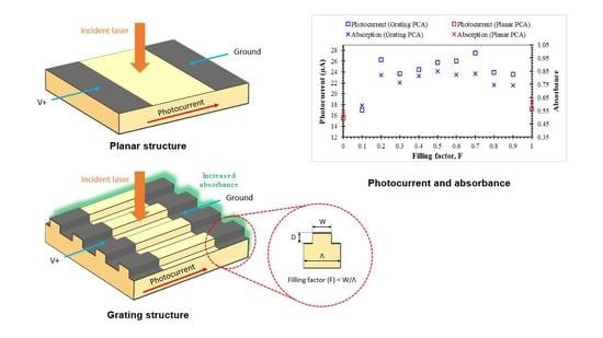
A PCA is an optoelectronic device which could be employed as both emitter and detector in a THz-TDS system [
13]. Their components and functions are shown in
Figure 1. The PCAs based THz-TDS system has an advantage of being able to operate at room temperature, while still achieving a coherent detection. These allow us to obtain broadband, high signal-to-noise ratio (SNR) signals containing both amplitude and phase information. While THz-TDS systems serve as potential equipment for future research and applications [
14], the main drawback of the PCA is its low optical-to-THz conversion efficiency, thus limiting the applications only in examining thin or low-absorbing specimens.
In recent decades, the significant advancement in nanotechnology has brought attention to the study of the nanostructured PCAs in order to improve their performance. Some examples are metallic nanoislands, plasmonic contact electrodes, and plasmonic nanostructures on the PCA structure [
15,
16,
17,
18,
19,
20,
21,
22,
23,
24]. Researchers have proved that the optical-to-THz conversion efficiency of the plasmonic based PCA greatly increases due to the local field enhancement and the reduction in thermal and carrier screening effects [
25,
26]. Another approach in improving the PCA output power is by depositing an anti-reflection coating, such as silicon nitride, titanium oxide, aluminum oxide, and zinc oxide nanorods, on the PCA surface [
27,
28,
29,
30,
31]. By estimation, a PCA on GaAs substrate with a perfect anti-reflection surface can totally suppress Fresnel reflection thus result in a 48% higher absorption and consequently enhance the THz power. Similarly, the anti-reflection effect of a PCA could be achieved by incorporating a grating structure into the photoconductive substrate. Compared to the anti-reflection coatings, a subwavelength grating has an advantage as the spatial distribution of the electric field could be optimized by engineering its geometrical parameters. Furthermore, it could also avoid the adhesion problem and other limitations induced from the exotic coating materials.
In this work, a new design of PCA consisting of the antenna electrodes deposited on a subwavelength grating low-temperature grown GaAs (LT-GaAs) substrate is proposed. The optical induced photocurrent of the proposed structure is simulated by using COMSOL Multiphysics, a commercially available finite element method (FEM) solver. The geometrical parameters of a grating PCA, such as period (Λ), filling factor (
F), and depth (
D), were varied and investigated through their electrical and optical responses. Based on the simulation results, this new design would improve the optical-to-THz efficiency up to 63%, compared to a conventional PCA. Besides, the proposed design also has an advantage in terms of fabrication as the fabrication techniques of both grating and antenna electrodes are already well-explored and formulated. In this article,
Section 2 explains the theory supporting this work,
Section 3 shows the developed simulation model,
Section 4 discusses the results, and conclusions of the work is given in
Section 5.
2. Theory
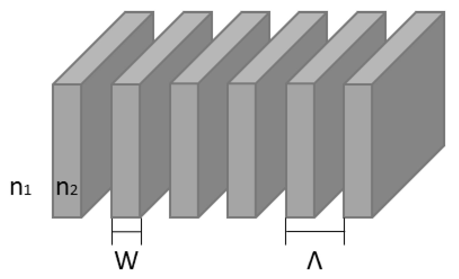
The effective medium theory (EMT) is applied to describe the interaction of light with a subwavelength grating as the grating structure (as illustrated in
Figure 2) can be well approximated as a homogeneous uniaxial layer posing an effective refraction index,
neff [
32,
33]. The effective index is affected by the grating parameters, the polarization of the incident light, and the refractive index of the surrounding medium. If polarization is not taken into account,
neff of the grating structure is represented by
where
n1 and
n2 are the refractive indices of the surrounding medium and the grating material, respectively. The filling factor,
F =
W/Λ, represents the volume fraction of the material with index
n2 whereas
W and Λ are the grating slab width and the grating period, respectively.
Equations (2) and (3) are used in estimating the
neff of the grating in the case where the incident light is polarized.
where
neff,|| and
neff,⊥ are the effective indices where the incident electric field vector is parallel and perpendicular to the grating slabs, respectively.
The following mathematical equations describe how the PCA performs. First, the electric field distribution in the simulation entity can be described and derived (in frequency domain) from Maxwell’s equations:
where
E is the complex electric field vector.
μr,
ϵr, and
σ are the relative magnetic permeability, electrical permittivity, and electrical conductivity of the material, respectively.
k0,
ϵ0, and
ω are the free-space propagation constant, the free-space permittivity, and the angular frequency of the incident wave, respectively. Note that
ϵr and
σ are based on Drude-Lorentz model, which includes the interband transition with Lorentz oscillation.
The incident electric field (4) with the total power
P is absorbed by the substrate and then free carriers are generated. Assuming that the laser has a Gaussian shape in a temporal dimension, the generation rate
RGEN can be defined as the following proportionality relation:
where
α is the spatially-dependent effective photon absorption coefficient of the substrate,
tc is the center of the Gaussian peak,
wt is the Gaussian width of the laser pulse,
h is Planck’s constant,
f is the incident frequency, and
Eg is the bandgap of the semiconductor substrate.
Although the laser illumination is uniform across the substrate, this does not imply that the generation rate is also constant due to the structure of the substrate. The refractive index mismatch between the substrate and air could cause the absorption and reflection of the incident electric field, which could change the electric field power and generation rate subsequently.
Once free carriers are generated, they will move along the direction of the bias electric field. The carrier dynamics can be solved by using Poisson’s Equation (6) and the continuity equations for electrons and holes, in time domain (7) and (8).
where
V represents the voltage distribution in the substrate,
n and
p are the electron and hole concentration,
q is the electron charge,
NA and
ND are the acceptor and donor ion concentration,
Jn and
Jp are the electron and hole current density, and
RGEN and
RREC are the generation and recombination rates, respectively, of both electrons and holes. Note that these rates are the same for both electrons and holes, as the generation/recombination of one carrier will induce the same effect for the opposite charge.
The current density of electrons and holes can be calculated by the drift-diffusion equations as:
where
μn and
μp are electron and hole mobilities,
Dn and
Dp are electron and hole diffusion coefficients, and
VDC represents a bias voltage. When the effective mass of the hole is much larger than the effective mass of the electron (which is usually the case), electron carriers will be much more sensitive to the external stimuli including substrate structure. The THz field,
ETHz, can be approximated from the magnitude of electron current density, ‖
Jn‖, by the following relation [
34]:
Note that changing the substrate structure could potentially induce the change of Jn which is affected by the generation rate, as seen from Equations (6)–(8). Therefore, the THz field intensity also depends on the structure of substrate.
3. Simulation Model and Methods
In this study, an FEM was applied to simulate a time-dependent current generated in a 3D grating PCA structure. In our approach, a commercial FEM-based computation tool, COMSOL Multiphysics Version 5.4 was used. The Semiconductor and Wave Optics modules were utilized and coupled to study the optical and electrical responses of a PCA. A single period of the grating PCA was modeled and solved by using periodic condition, as it would greatly reduce the computational burden. The incident laser field was specified in the Wave Optics module, and the bias voltage was defined in the Semiconductor module.
Figure 3 illustrates the proposed grating THz emitter structure and the developed simulation model. The geometrical parameters of the model are summarized in
Table 1. As defined previously,
F is the ratio of
W to Λ. There are two materials defined in the simulation model, i.e., GaAs (blue) domains and air (transparent) domains, with their material properties imported from an existing library of the simulation software. To be specific, the intrinsic properties of GaAs were used, where
μn and
μp were equal to 8500 cm
2/V·s and 400 cm
2/V·s, respectively. No doping profile is added to the material; hence,
NA and
ND are equal to zero. To ensure numerical stability, the coarsest mesh was set as 6 elements per GaAs refractive index per wavelength.
The incident wave was defined as a periodic port at the air surface with a wavelength of 780 nm, a peak power of 10 mW, and a Gaussian time profile of 100 fs pulse width with 300 fs delay time. In the port setting, the electric field mode was selected, and the incident wave was set to be perpendicular to the grating groove by enabling only the z-component of the electric field, Ez. A continuity periodic condition was set for the side walls of the grating in parallel with the x-axis to make the electric field equal on both the source and destination boundaries. This was done to simulate the behaviors of other grating periods without significantly increasing computation. The antenna was defined as two ideal ohmic contacts with a bias voltage of 20 V. A Shockey-Read-Hall (SRH) model trap-assisted recombination with an ultrashort lifetime of 1 ps was added to imitate the well-known material behavior of PCA, LT-GaAs. The Optical Transitions node in the interface configured the coupling between two interfaces to compute the carrier generation and recombination rates.
By using a frequency-transient study in time domain, the photocurrent generated in grating PCA model was computed in a range of 5 ps with a time step of 20 fs. In order to observe the grating effect, the absorbance, reflectance, and transmittance were measured at the port on top and bottom of the designed PCA. A conventional planar PCA was modeled by setting F to 1 and compared with the proposed grating PCA structure. The parametric study of the grating PCA was carried out by varying Λ, D, and F. Note that only one parameter was varied at a time, while the other two were fixed.
4. Result and Discussion
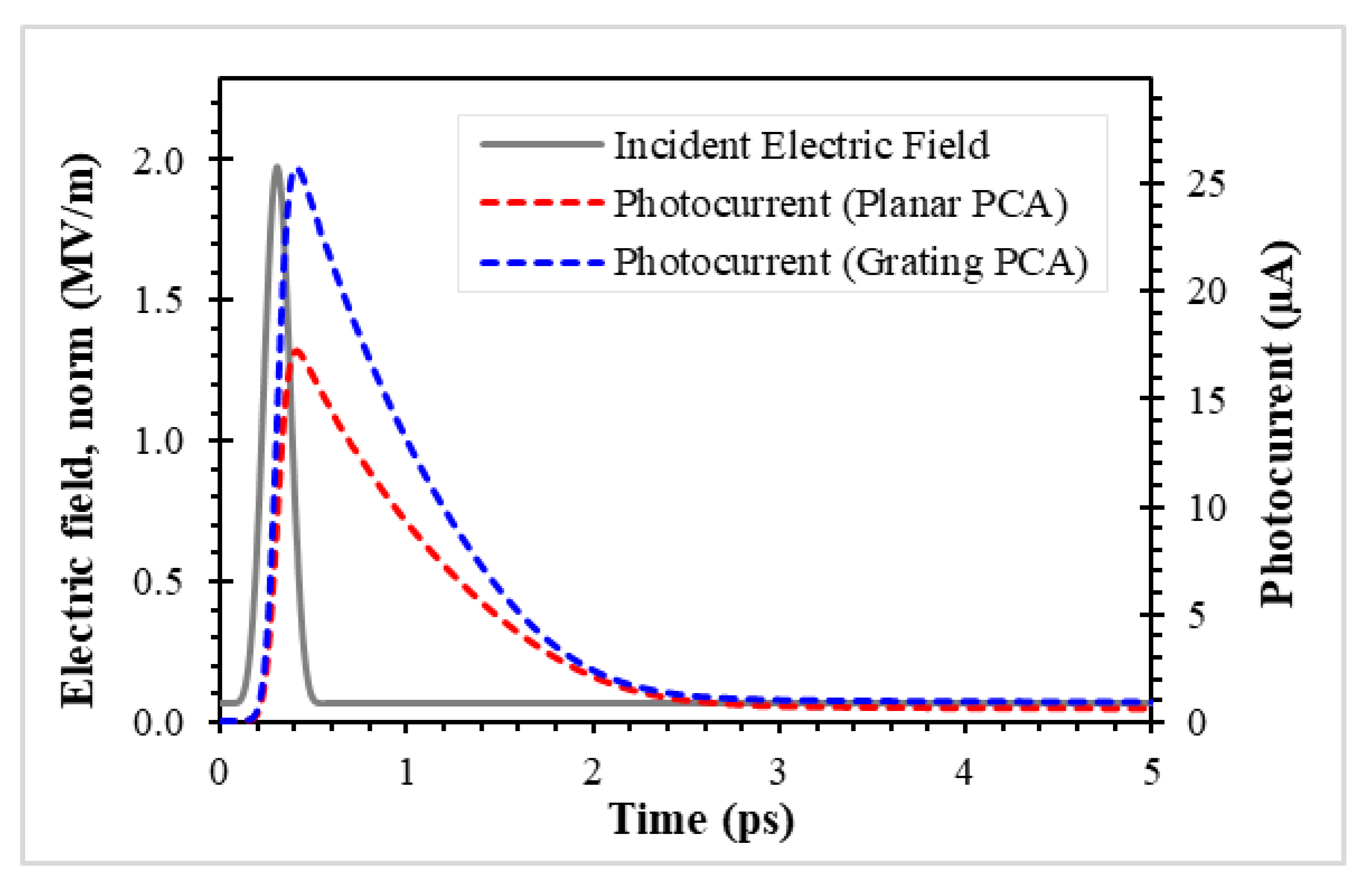
The THz signal generated by a PCA emitter is indirectly observed via induced photocurrent from a simulation as mentioned earlier in this study.
Figure 4 shows the computational results of the simulated grating and planar PCA models. For both PCAs, the magnitude of electric field (i.e., norm) of a 780 nm-incident pulse, probed at the center of excitation port, shows a maximum amplitude of approximately 2 MV/m with a peak position at 300 fs. The induced transient photocurrent drastically increases at a rate approximately proportional to the optical pulse and decreases afterward by the effects of trap-assisted recombination. In both PCAs, there is no significant difference in the pulse width of the photocurrent as it is determined by the recombination lifetime and the photoconductive gap between the electrodes. Based on simulation results, the calculated peak photocurrent of the grating PCA is 25.75 µA, which is approximately 50% larger than that of the planar PCA (peaked at 17.19 µA).
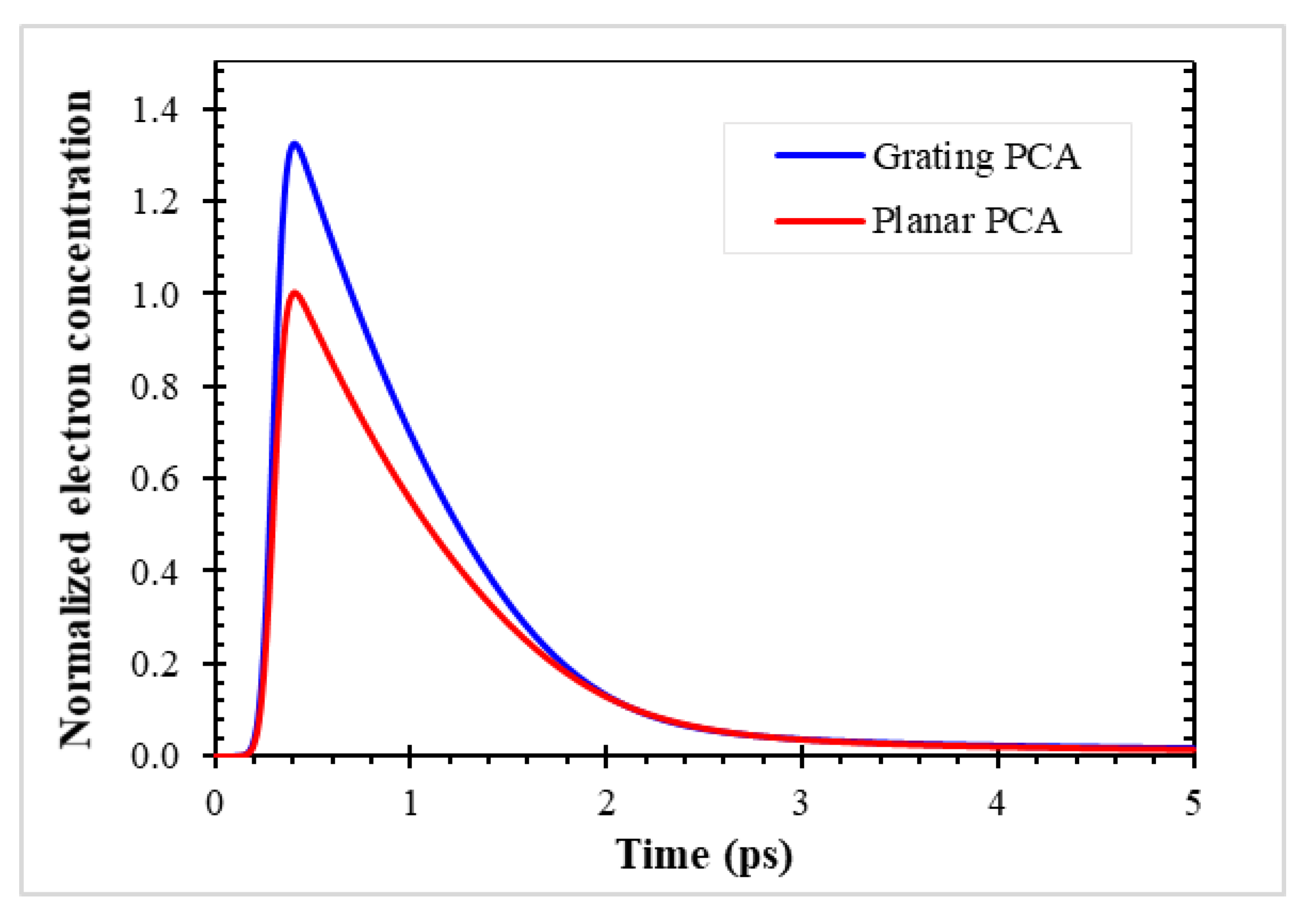
The enhancement of the induced photocurrent is explained through the increase in generated carrier concentration,
n, in the grating PCA.
Figure 5 shows the normalized total free electron carriers in both PCA models with respect to time. Observe that their rise times are similar: the peak amplitudes are located at approximately
t = 400 fs, which is shortly after the peak amplitude of incident wave. This is due to the same photocarrier generation time in both PCAs.
Figure 5 suggests that the grating PCA yields 32% more free electron carriers compared to that of the planar PCA. By comparing
Figure 5 to the photocurrent in
Figure 4, the decay of the photocurrent appears to correspond to the changes in
n.
As explained in
Section 2, the electrical responses of the PCA are results from its optical response. The optical response of the simulated PCA is illustrated by the electric field distribution in the model.
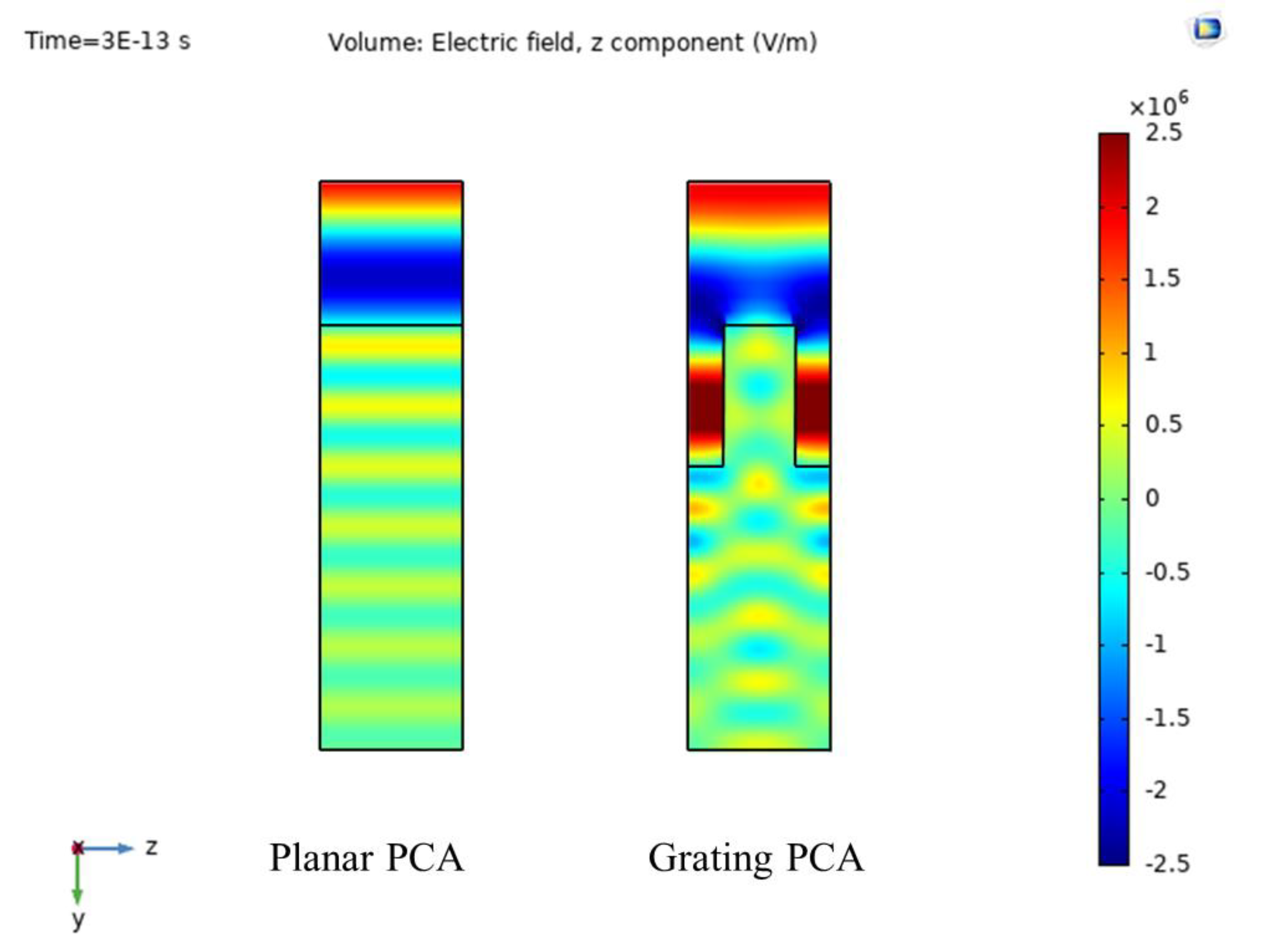
Figure 6 shows the spatial distribution of the z component of the electric field,
Ez, in the planar and the grating PCA models. For both structures, a higher magnitude of
Ez is found in the air domains compared to the substrate. Unlike the planar PCA, a diffraction pattern appears in the grating structure. Based on the results, a higher intensity of
Ez with a maximum magnitude around 1.69 MV/m is found in the grating PCA substrate, compared to the planar PCA. The maximum magnitude of
Ez in the planar PCA is 0.74 MV/m. The results indicate that the planar PCA has a lower optical absorbance, despite its larger active area.
The grating PCA yields a higher photocurrent compared to the planar PCA because of their corresponding absorbance. Here, the optical property of a grating structure is investigated. The absorption in LT-GaAs and the reflection at the interface can be explained by the following Fresnel’s reflection equation:
where
A is the absorbance, and
R is the reflectance at the interface. By substituting
n1 = 1 (air) and
n2 = 3.685 (LT-GaAs at 780 nm), the reflectance and absorbance of a planar PCA are 0.328 and 0.672, respectively. By using Equation (3), where the electric field is perpendicular to the grating slabs,
neff,⊥ of a grating PCA is equal to 1.3648 for a grating structure with
F = 0.5 (as shown in
Figure 7). Note that the values of
n1 and
n2 used in the calculation are the same as those in COMSOL simulation model, however only the real part of the refractive index is used in the calculation.
Table 2 lists the reflectance and absorbance obtained by a calculation and a simulation. Both results show that the grating PCA has a smaller reflectance and a larger absorbance than those of the planar PCA. These results confirm a higher laser absorbance due to the anti-reflection effect from
neff in the grating structure.
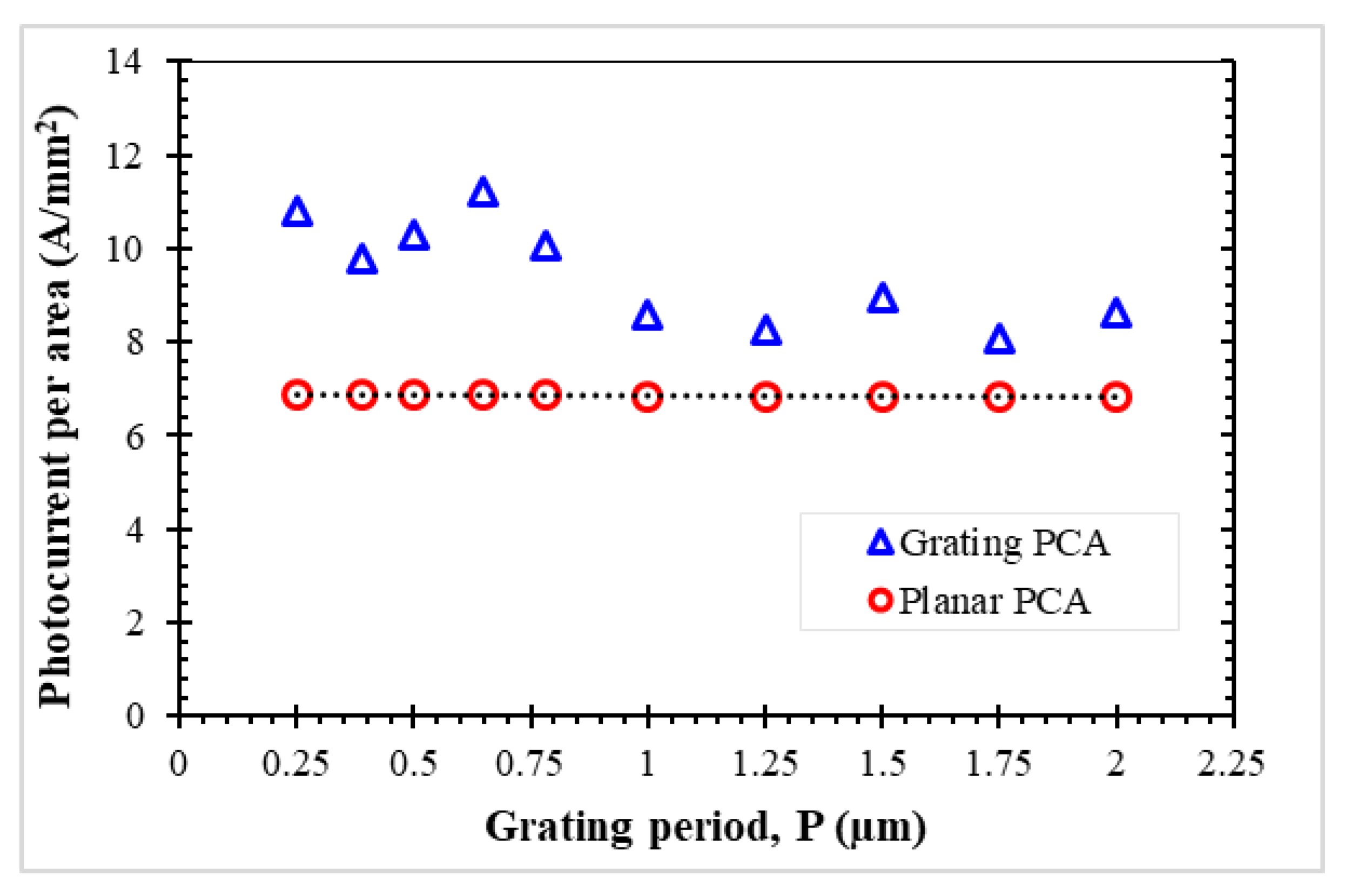
The effects of Λ in the grating PCA are investigated by varying the value of Λ from 0.25 µm to 2.0 µm. To ensure the same peak intensity applied, for all cases, the power of the incident laser is normalized by the area of the air domain, i.e., a larger Λ structure is excited with a higher laser power.
Figure 8 represents the induced photocurrent per laser illuminating area in the grating PCAs and the corresponding planar structures. Apparently, the photocurrent of a planar PCA is not influenced by the parameter Λ. As such, the value of photocurrent per area is ranging from 6.85 A/mm
2 to 6.88 A/mm
2. Based on the simulation, the resulting photocurrent of a grating PCA is always higher than that of the planar PCA. Contrary to the planar PCA, Λ greatly affects the THz output signal of a grating PCA, especially the cases of Λ smaller than the incident laser wavelength. The increment factor is defined as a ratio of the induced photocurrent in the grating PCA to that of the planar PCA. For the cases of Λ ≤ 780 nm, the increment factor is ranging from 1.43 to 1.63. The increment factor when Λ > 780 nm is ranging from 1.18 to 1.31. This indicates that a smaller Λ structure can better enhance the THz emission of a PCA.
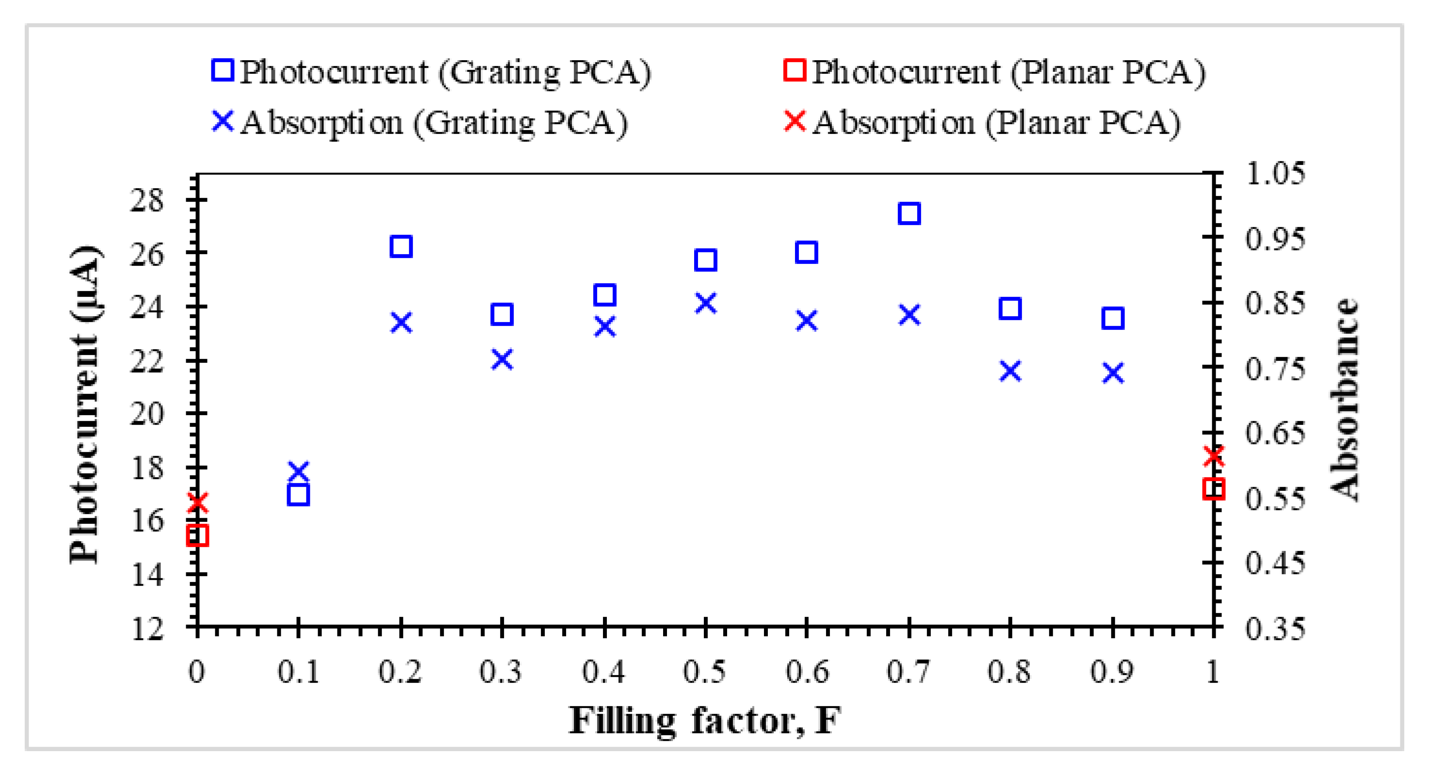
Next, the effects of parameter
F in a Λ = 0.5 µm grating PCA are investigated by varying
F in
Table 1, from 0.1 to 0.9, with a step size of 0.1. Cases of
F = 0 and
F = 1 are the planar PCA with a substrate thickness of 1.0 µm and 1.5 µm, respectively.
Figure 9 shows the photocurrent and the optical absorbance of the grating PCA with all values of
F. The simulation results show that the case of
F = 0.5 exhibits the best absorbance of 0.851 of the incident wave. The optical absorbance of 0.831 at
F = 0.7 is slightly less than that at
F = 0.5, and it has the highest photocurrent among all studied cases, 27.46 µA. Compared to the planar PCA (
F = 1), all the grating PCAs, except at
F = 0.1, exhibit a significantly better absorbance and, thus, photocurrent, with the increment factors of 1.37 to 1.60.
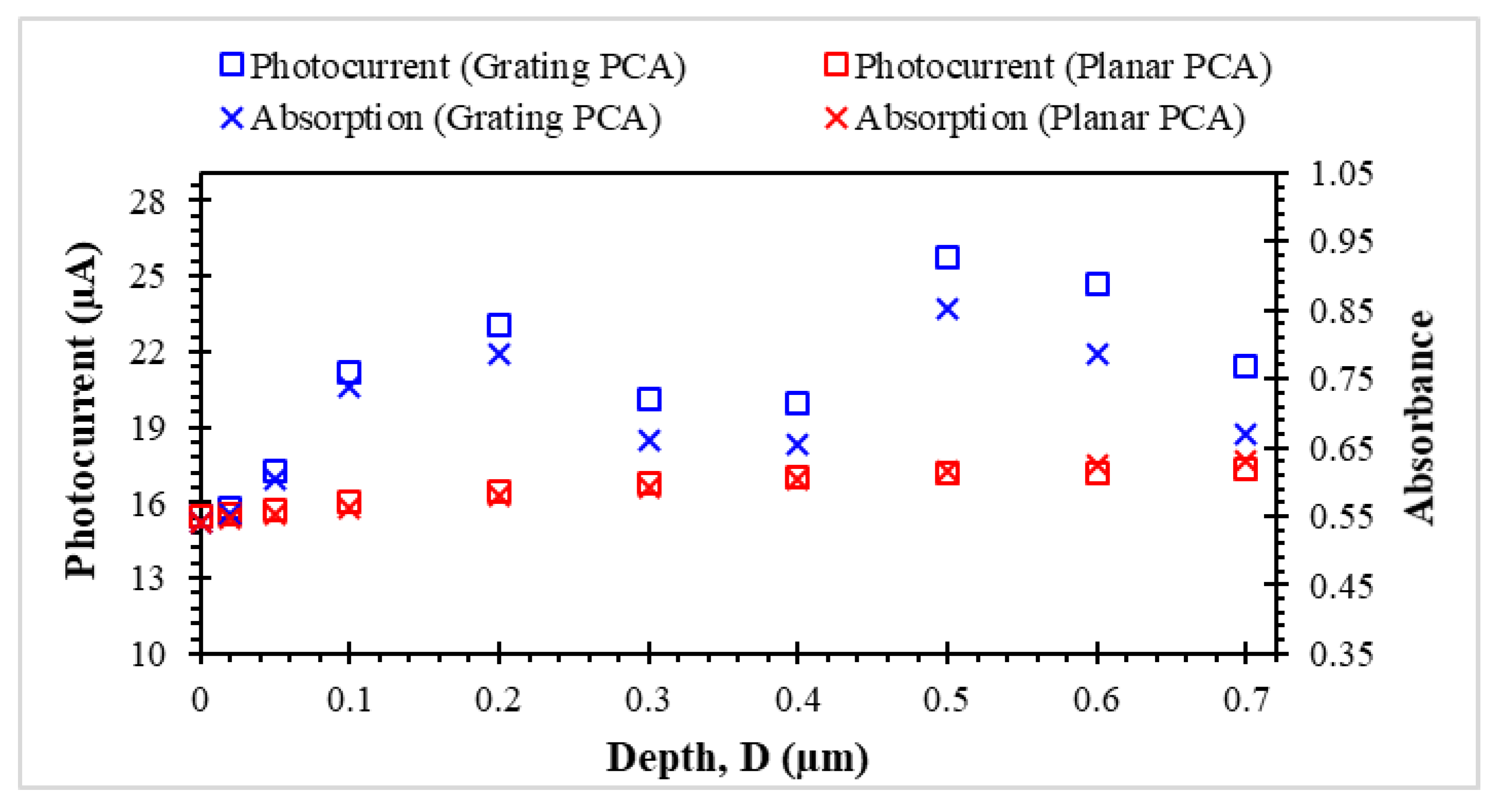
The last parameter of our interest,
D, is studied for the grating structure by varying
D in
Table 1, from 0 µm to 0.7 µm, where 0 µm is the planar PCA with a thickness of
H only. Note that Λ = 0.5 µm and
F = 0.5 are used here. According to
Figure 10, for the planar PCA, the photocurrent tends to increase with respect to the increase of the LT-GaAs substrate thickness. This increment becomes less significant when
D is large enough. For example, there is only 0.007 µA difference between
D = 0.6 µm and
D = 0.7 µm, whereas there is 0.59 µA difference between
D = 0 µm and
D = 0.1 µm. For the grating PCA, there is always an apparent improvement in the induced current compared to that of the planar PCA, especially when
D ≥ 0.5 µm. The increment factor for
D ≥ 0.5 µm is observed to range from 1.10 to 1.50.
Nonetheless, the increase in
D for a grating PCA shows a non-descriptive trend in the simulated photocurrent, unlike the planar PCA. However, we can see a strong correlation between the photocurrent and the absorbance of a grating. This confirms that the increase in the photocurrent is due to the increment in the incident wave absorption. Still, the results show that the optical properties of a grating PCA are greatly influenced by the geometrical structure of grating. The earlier research work has proved that the reflected intensity of a dielectric surface-relief grating strongly depends on the groove depth [
35].


