1. Introduction
Shining metal nanoparticles (NP) with light of much greater wavelength than the NP size lets the free electrons in the metal generate oscillations called localized surface plasmons (LSPs) that restrict the geometry of NP [
1]. The momentum of the photons is not required to match the free electron momentum and direct illumination at any angle can induce the LSPs in the metal NP [
1]. At resonance, the amount of intensity or wavelength of the resonance peak is sensitive to any change in the dielectric property of the NP’s surrounding medium, as explained by Mie scattering theory [
1]. So, this direct excitation mechanism makes this type of sensor far less complex than the regular SPR sensor that works under the total internal reflection (TIR) principle [
2]. Furthermore, exciting in the normal angle helps in miniaturization of the localized surface plasmonic resonance (LSPR) sensor system and lower costs are expected compared to the SPR sensor. In addition to that, the LSPR sensor system offers better local detection of dielectric property changes than the regular SPR sensor [
3]. Simplicity in the excitation mechanism, and sensing setup, and the lower cost of the LSPR sensor make it superior to the SPR sensor and for decades this attracted this researcher’s attention.
When the refractive index of the medium surrounding the metal NP changes, the amount of absorption and the resonance wavelength alter as confirmed by Mie scattering theory [
1]. The performance of LSPR sensor then can be assessed by measuring how much shift (either in resonance intensity or resonance wavelength) resulted due to change in the refractive index of the metal NP’s proximity, as in Equations (1) and (2) [
4].
where
and
are sensitivity-based on wavelength and intensity shift respectively.
,
, and
are the change in the sensing medium’s refractive index, the resonance wavelength (nm), and the resonance intensity, respectively.
The figure of merit of the LSPR sensor can be assessed using Equations (3) and (4) [
4].
where
are figures of merit based on wavelength and intensity shift respectively and FWHM is the full width at half maximum of the resonance band.
Though the LSPR sensor has a good advantage over a regular SPR sensor, its low performance restricts its commercialization. Reduction in sensing performance is due to an increase in resonance peak width resulting from the damping process in the localized plasmons modes [
4,
5,
6]. So far, researchers continue to try to enhance performance in different ways, through engraining the geometry of the NP and material type. However, recently, gold-graphene hybrid nanostructure has become a promising field in overcoming the performance issue of LSPR sensors, as briefly reviewed in our recently published review paper [
7]. In one of our published works [
8], it has been shown that a spherical gold-graphene core-shell NP array produces a sharp resonance mode in the near-infrared (NIR) region with FWHM of 8.1 nm. This sharp resonance enhances the figure of merit (FOM
λ) of the sensor up to 102.6, which is an extremely significant enhancement in the field of gold-graphene hybrid nanodevices. Another study, also conducted by our group at Waterloo, introduces an impeding graphene film between gold NPs arrays [
9] to enhance the sensor performance (FOM
I = 256) more than two-fold, compared to the core-shell structure, which is a fairly high improvement with respect to LSPR sensor performance. However, fabricating these nanostructures and others which are similar to those in existing literature, is still under development, especially in producing graphene in 3D (as in core-shell).
From an engineering point of view, the optimum choice is to design a device with high performance and low cost, and which is reproducible. As known, the main issue of the LSPR sensor is its performance, and higher performances are achievable either in a complex hybrid scheme or a simple one. By studying the effect on the sensing performance of randomly spin-coated graphene flakes on top of and between the gold NDs array, this article aims to answer the question of whether LSPR sensor performance can be improved using a simple hybrid scheme. This proposed hybrid scheme is fabricated in only three fabrication steps starting with gold film deposition, followed by direct milling using a focused ion beam technique, and then spin coating graphene solution using a spin coater. These fabrication steps are well studied in literature and have good controllability, as reported elsewhere [
10,
11]. Having few and controllable fabrication steps is the advantage of this proposed sensor and the resulting good performance of the sensor is described in this work. In the following sections, the method used to conduct this research is explained and the results obtained and applications of the sensors are also discussed. Finally, some considerations for further optimization work are discussed followed by the conclusion.
2. Methodology
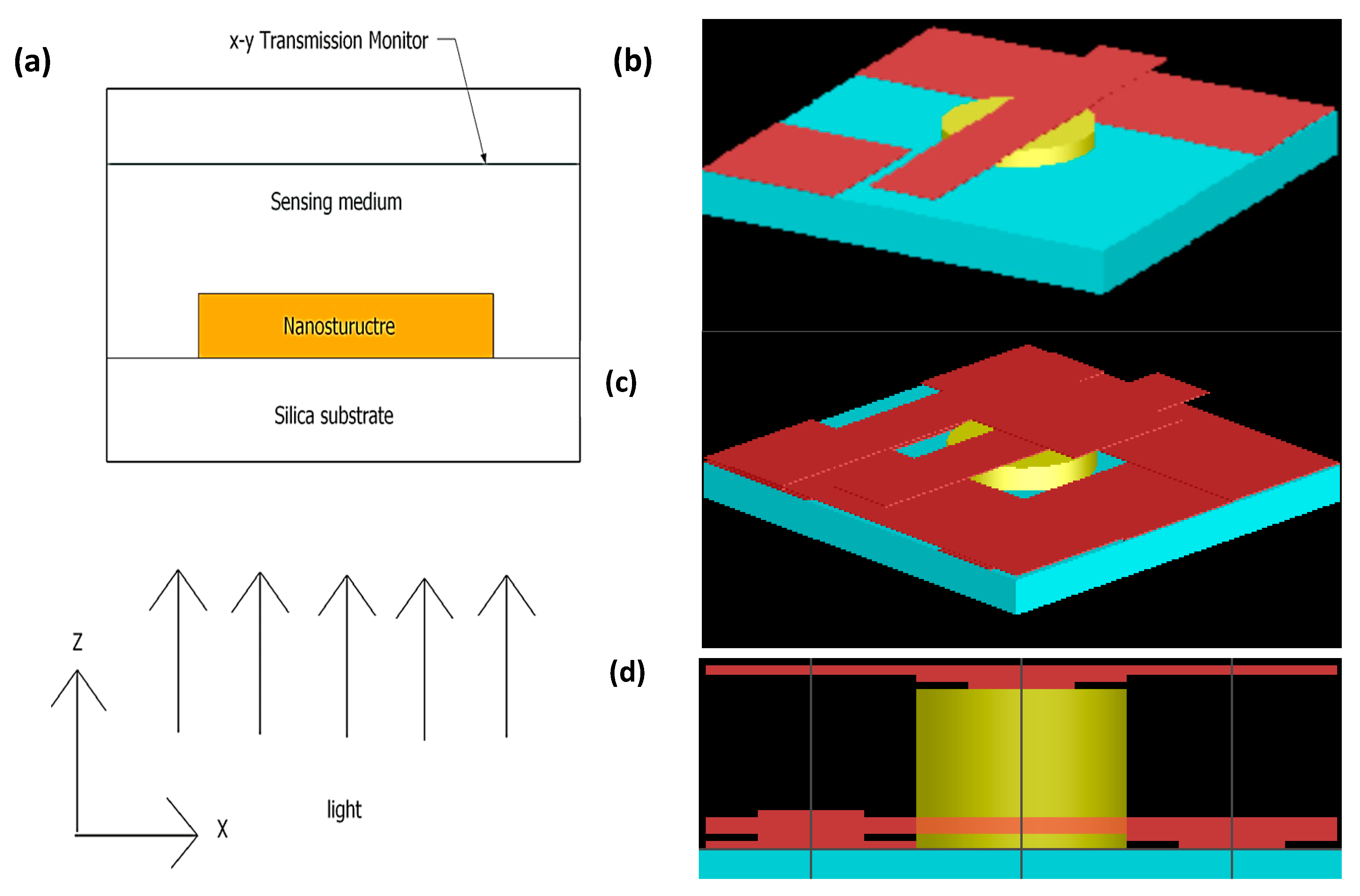
This study was performed by solving Maxwell’s equation using the 3D full wave vector finite difference time domain (FDTD) method to calculate the light absorption spectra of the Au-G hybrid nanostructure placed on top of quartz substrate, as schematically shown in
Figure 1a.
Figure 1b shows a 3D view with only three graphene flakes,
Figure 1c shows a 3D view with the total number of graphene flakes (10 flakes), and
Figure 1c shows a cross-section of one unit of Au-G hybrid nanostructure that repeated periodically in x and y directions. The hybrid nanostructure involves a Au NDs (diameter = 100 nm, height = 20 nm) array with periodicity of 300 nm placed on substrate and then graphene flakes with different shapes and sizes (rod (50 × 300 nm), square (100 × 100 nm), and rectangle (100 × 300 nm)) placed randomly on top and between Au NDs as shown in
Figure 1b,c. The thickness of the graphene flakes is 1 nm. The assumption is, that graphene flakes in solution do not come in similar shapes or sizes.
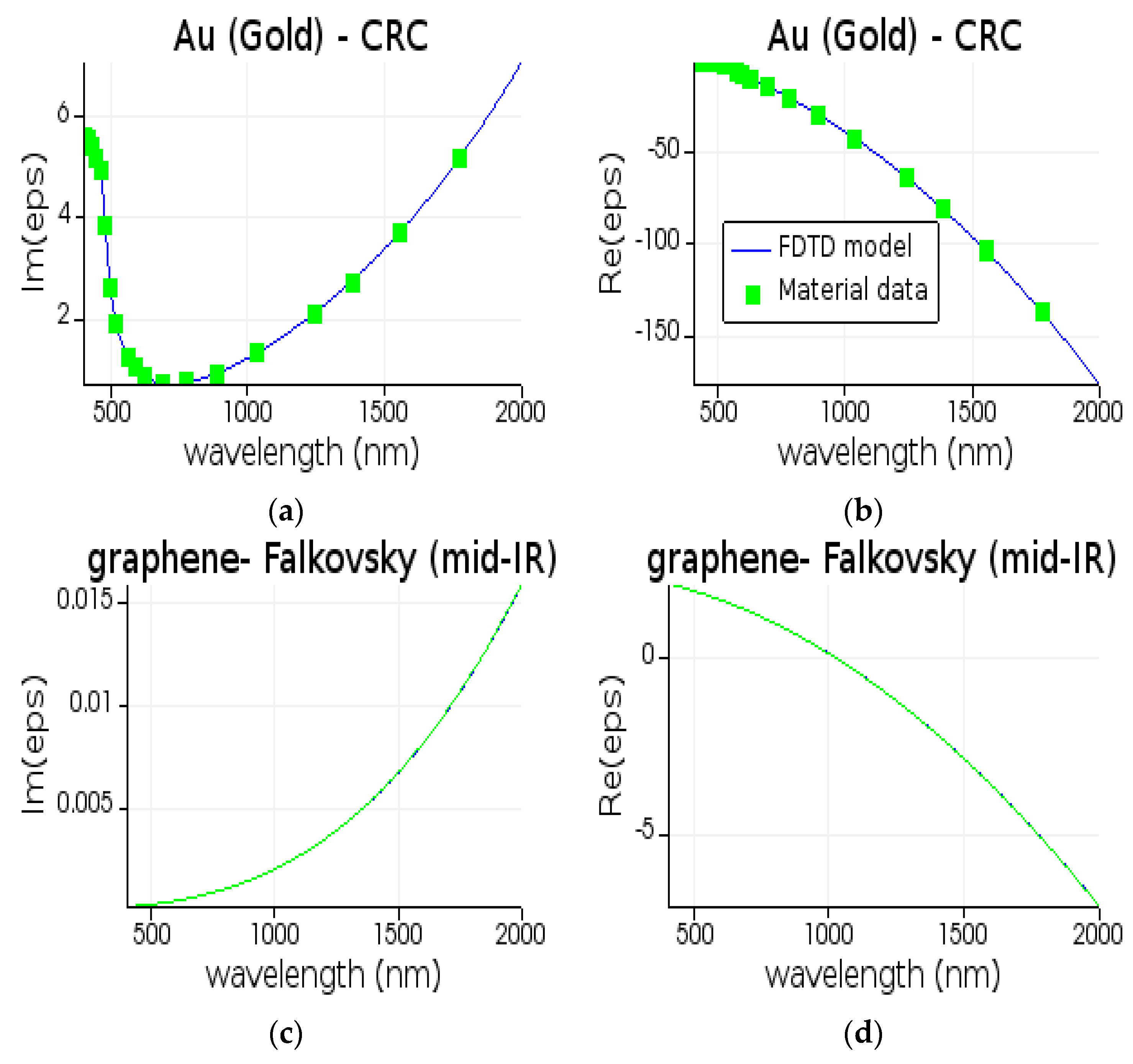
Dielectric properties (permittivity) of gold and graphene are calculated using the Drude-Lorentz model and fitted with experimental values of real and imaginary part of gold permittivity given by [
12] and graphene which was obtained from the Falkovsky model [
13], as shown in
Figure 2, where good fitting enhances the confidence level of obtained results. For the substrate, silica (quartz) with fixed refractive index of 1.45 is used and the background is set to n = 1 (air).
A commercial software package (Lumerical FDTD Solutions) is used to carry out the numerical analysis. All Au ND-G flake hybrid nanostructures, transmissions, and plane wave sources are co-planned with boundary conditions that made them infinite in the x- and y directions. Herein, as shown in
Figure 1a, the nanostructure is illuminated from the bottom by an unpolarized plane electromagnetic wave that is used as the light source. The electromagnetic wave propagates in the z-axis (as labeled by arrows in
Figure 1a) in the wavelength range of 0.4 to 2 μm with electric field amplitude of 1 V/m. Asymmetric and symmetric boundary conditions are used in the x and y axes, respectively, instead of periodic boundary conditions, to reduce calculation time, and perfect matched layer boundary condition is used in the z axis. The mesh cell size (calculation grid resolution) is very small (0.035 nm point-to-point distance) in the z direction to make sure that we get enough resolution due to the presence of graphene flakes with a thickness of 1 nm (~ three graphene layers). In x and y axes the mesh cell size was 5 nm. The simulation time is set to 500 fs. The source is placed 250 nm below the substrate-Au ND interface and to calculate absorption spectra, an x-y monitor is placed 150 nm above the Au ND-substrate interface. Another x-z monitor is used to calculate the cross-section electric field profile of the nanodevice. Air (n = 1) is chosen as the sensing medium for sensing measurement.
In this work, the effect of graphene flakes placed randomly on top of and between Au NDs arrays is studied by comparing the absorption spectra of only Au NDs arrays with Au ND-G flakes hybrid nanostructure where all the size and shape parameters of both of Au ND and G flakes are constant. Then, the sensitivity of the hybrid device is measured by monitoring the shift in resonance wavelength as the refractive index of the sensing medium changed from 1 to 1.04 with 0.01 steps. Sensitivity of the sensor is assessed by the ratio of wavelength resonance shift to refractive index change (Equation (1)). Further optimization suggestions and applicable applications for the proposed sensor are discussed below.
3. Results and Discussion
The absorption spectra of Au NDs arrays placed on top of quartz substrate are calculated in the wavelength range of 400–2000 nm (
Figure 3a). Then a number of graphene flakes with different shapes and sizes are distributed around Au NDs to a total thickness of 5 nm (each flake thickness = 1 nm) and only three flakes (total thickness of flakes = 3 nm) are placed on top of the Au ND, as shown in
Figure 1b. The absorption spectra for the Au ND-G flake’s hybrid nanostructure is then calculated and compared with spectra of Au NDs only as shown in
Figure 3a.
Absorption spectra of Au NDs arrays show strong resonances in the visible region (at λ = 642.4 nm), which could be attributed to the intrinsic absorption property of gold where red shift due to the geometrical dependence of the gold ND [
14], and other resonances may be attributed to different LSPR modes [
15]. After adding G flakes, changes take place in resonance intensity and wavelength and other new resonances are created. In the visible region, no enhancement in the absorption is recorded, while it is present in longer wavelength resonances (resonances between 750–1100 nm). This may be attributed to the optical graphene losses that increase in the visible region, and decrease in longer wavelength resonances [
16]. In addition, in the visible region, no apparent shift in the resonance’s wavelength is present after spin-coating graphene flakes, while it is clearly observed in longer wavelength resonances. In the visible region, absorption of gold is due to intrinsic absorption, while in longer wavelength resonances (750–1100 nm) it is due to interaction between NPs, and thus, it is expected that shifting in the resonance’s position will occur due to change in the size and shape of the nanostructure. As reported by Mu et al. [
17], the resonances in the NIR could be blue-shifted due to the charge transferred between graphene and gold, which is observed here in the resonances between 750–1100 nm. The more interesting observation here, is obtaining new resonances in the region ~1100–2000 nm, where there are no resonances recorded for Au ND array. Two resonances observed here are: a sharp one at 1203.81 nm and a broad one at 1882.28 nm. These two resonances result from the coupling of Au and graphene flakes resonances as shown in the electric field profile,
Figure 3b,c at λ = 1203.81 nm.
Figure 3b illustrates the cross-sectional electric field profile for Au ND, while
Figure 3c shows the profile for Au ND-G flakes hybrid nanostructure. There is ~200% enhancement in the electric field after adding of graphene flakes on top of gold NDs at λ = 1203.81 nm. The observed enhancement is due to strong localization of the field which is clearly observed at the bottom side (right and left) of gold ND is in good agreement with literature, as, for example, reported by Benjamin et al. [
18]. They introduced a large-scale self-organized gold nanostructures fabrication technique and studied the nanoparticles plasmonic resonances for SERS application. They found that significant enhancement in the SERS signal (~1200 times) contributed to absorption observed through spectroscopy ellipsometry measurements due to LSPR effect. Strong localization is a good indication of a highly sensitive sensor. Therefore, a sensitivity measurement is conducted by changing the refractive index of the sensing medium and monitoring the shift in resonance mode A and B to calculate the sensor sensitivity as detailed in the following section.
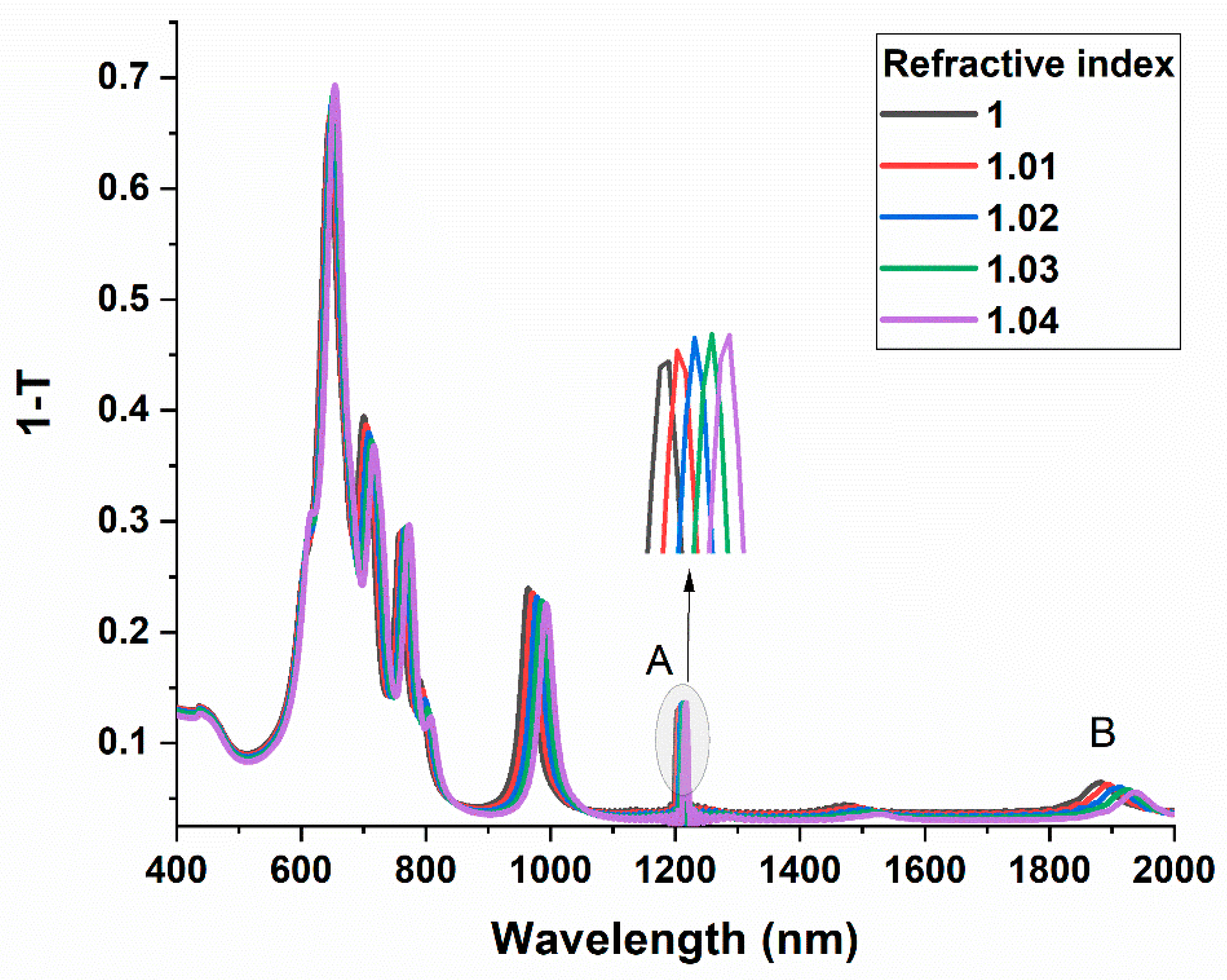
Sensing measurement is done by calculating the absorption spectrum of the hybrid nanostructure at different values of the refractive index of the sensing medium and monitoring the shift in resonances modes A and B, as indicated in
Figure 4. The sensitivity of the sensor under study is then calculated using Equation (1). The refractive index of the sensing medium increased from 1 to 1.04 with 0.01 step.
Figure 4 represents the spectrums of the gold-graphene flakes hybrid nanostructure at different refractive indices, and clearly shows resonance shift in intensity and wavelength for all resonances in the spectrum. Shifting in the resonance can be explained using Mie scattering [
1]. According to Equation (5), when permittivity of the medium of NP proximity changes, the resonance changes linearly. As shown in
Figure 4, mode A redshifted from 1203.81 nm to 1217.35 nm when the refractive index of the sensing medium increased from 1 to 1.04.
Multispectral properties (different plasmonic modes) of our proposed sensor as shown in
Figure 4, can improve the sensor performance better than devices with only one resonance mode. From
Figure 5, resonance mode A shifted by an amount of ~2.6 nm, and resonance mode B by an amount of ~8.9 nm, when the refractive index of the sensing medium increased from 1 to 1.04. This leads to different sensitivities for different plasmonic resonance modes.
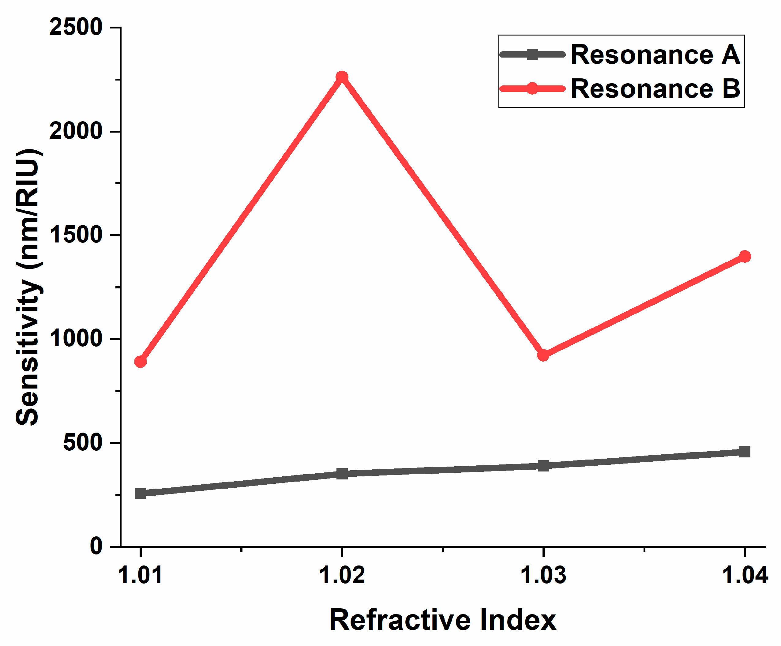
Figure 6 illustrates the sensitivity of the proposed nano-device for each change in the refractive index of the sensing medium using resonances A and B. The sensitivity is calculated using Equation (1). As mentioned, longer resonances exhibit greater resonance shift, and thus higher sensitivity results. The resonance A at λ = 1203.81 nm demonstrates a shift of approximately 3 nm for each change in the refractive index, and maximum sensitivity of 457 nm/RIU results when the refractive index of the sensing medium is changed from 1.03 to 1.04. However, the resonance B at λ = 1882.28 shows larger shifts for refractive index changes, and maximum sensitivity is recorded for resonance B at 2262 nm/RIU when the refractive index is changed from 1.01 to 1.02, where the resonance shift is approximately 21 nm. Using Equation (3), the figures of merit for both resonances A and B were calculated. The FWHM for resonance A is 6.5 nm and results in FOM of 70.3, while in resonance B the wide resonance peak width with FWHM of 54.9 nm yields an FOM of 41.2. Even though resonance B is associated with higher sensitivity, increase in the FWHM of the resonance band results in ~40 % reduction in the FOM compared to resonance A. Thus, mode A shows a better detection limit than mode B due to higher FOM; and moreover, in terms of sensitivity, mode B is more enhanced and further optimization in the structure aimed at reducing linewidth of the resonance B could enhance its FOM. The gold-graphene core-shell hybrid NPs array studied earlier [
8] shows 350 nm/TIU sensitivity and 102.6 FOM. The sensors undertaken in this work show more than 6 fold enhancement in the sensitivity using mode A, and ~ 40% reduction in the FOM using mode B. Thus, enhancing resonance B by reducing its FWHM by further optimization gives our sensor another advantage in addition to simplicity in fabrication, compared to core-shell structure.
The proposed gold-graphene hybrid nano-device shows competitive sensing performance in the field of LSPR sensors, in addition to its fabrication simplicity and controllability in comparison to those sensors that include continuous graphene film. The sensor discussed in this research can be manufactured through three main steps using pre-prepared graphene solutions [
19,
20]. The first, is gold film deposition followed by direct-milling, using well-known and widely used focused ion beam (FIB) technology [
21]. Then graphene solution is spin coated using a spin coater on top of the fabricated Au ND array. Significant improvement in sensing performance is observed numerically here; and the simplicity and controllability of the proposed nanostructure make this sensor superior for number of applications and, thus, enhance the commerciality of the LSPR sensors.
The sensing mechanism in SPR sensors is based on resonance angle shift due to refractive index change in the sensing medium. There is a similar scenario in the LSPR sensors, but instead of resonance angle there will be a shift in resonance wavelength or resonance intensity. Therefore, any application using the SPR sensors could use the LSPR sensors with different sensing mechanisms. The LSPR sensors can be used as immunosensors that are able to detect human growth hormone (hGH) in real serum samples. Makaraviciute et al. studied the application of SPR immunosensor using protein G based site-directed antibody capture technique (where protein G is a common used affinity capture reagent [
22]). Addressing direct repeated real sample measurements [
23]. Makaraviciute et al. performed the immobilization on top of the gold film. This can also be done on top of Au ND-G flakes hybrid nanostructure studied here, and the shift in the resonance wavelength or intensity after capturing hGH monitored. Furthermore, the SPR sensors show pretty good applicability in detecting DNA hybridization [
24], and in early cancer detection [
25]. Thus, immobilization and functionalization of Au ND-G flakes nanostructure instead of Au film as in SPR sensors, makes the proposed LSPR sensor studied here a good platform for biomolecular interaction detection that helps in detecting cancer diseases in early stages.
So far, the results of the proposed device are merely to prove that by spin-coating graphene flakes randomly on top and between Au NDs arrays, the sensing performance of the LSPR sensors can be increased. However, there are several points that need to be considered in further optimization of these sensors at the fabrication stage. The size and the shape, and the periodicity of gold NPs are effective parameters used to optimize sensing performance. Furthermore, size, shape, and thickness of graphene flakes are also effective optimization parameters that can be included in an apparent rule of optimization. For example, according to our previous study of gold graphene core-shell hybrid NPs [
8], increased thickness of graphene could enhance the resonance intensity and thus sensor performance. So, increasing graphene flakes thickness is one of the further optimization steps for the proposed sensor. In the fabrication stage, both the periodicity of the Au NPs and dimensions of graphene flakes should be carefully considered. In this work, the graphene flakes dimensions are in range of 100s nm, and periodicity of the gold NPs array is 300 nm. It is, therefore, possible that graphene flakes can be inserted between gold NPs, and that this insertion will enhance the interaction with light through increasing absorption. If the graphene flakes are larger than their periodicity, the effect of hybridizing may not give the expected results shown here. Therefore, optimizing periodicity according to produced graphene flakes dimensions is important to ensure better results in sensor sensitivity. In this study, the total size of graphene flakes is kept constant (fixed number of flakes) and incorporating more graphene flakes could enhance the absorption of the sensors and result in better sensing performance.


