Article

Design Investigation of 4 × 4 Nonblocking Hybrid Plasmonic Electrooptic Switch

1
Institute of Laser for Postgraduate Studies, University of Baghdad, Baghdad 10, Iraq
2
College of Engineering, Al-Nahrain University, Baghdad 10, Iraq
*
Author to whom correspondence should be addressed.
Photonics 2019, 6(2), 47; https://doi.org/10.3390/photonics6020047
Submission received: 23 February 2019 / Revised: 27 April 2019 / Accepted: 28 April 2019 / Published: 3 May 2019

Abstract

:
This paper proposes a compact, plasmonic-based 4 × 4 nonblocking switch for optical networks. This device uses six 2 × 2 plasmonic Mach-Zehnder switch (MZS), whose arm waveguide is supported by a JRD1 polymer layer as a high electro-optic coefficient material. The 4 × 4 switch is designed in COMSOL environment for 1550 nm wavelength operation. The performance of the proposed switch outperforms those of conventional (nonplasmonic) counterparts. The designed switch yields a compact structure ( 500 × 70   µ m 2 ) having V π L = 12   V · µ m , 1.5 THz optical bandwidth, 7.7 dB insertion loss, and −26.5 dB crosstalk. The capability of the switch to route 8 × 40 Gbps WDM signal is demonstrated successfully.

1. Introduction

Optical switches are key elements in advanced optical networks due to scalability, compactness, reliability, and ability to realize reconfigurable communication for on-chip optical networks [1]. They can be designed to perform different functions in the optical domain, including signal and wavelength-selective routing [2,3]. Generally, these functions require a high-order (N × N) optical switching platform, which relies on a matrix of 2 × 2 optical switching units [4,5]. Different configurations and material systems have been reported in the literature to design and implement the 2 × 2 optical switches but most of them stand heavily on silicon photonic-based Mach-Zehnder (MZ) configurations supported by thermo-optic [6,7] and electro-optic (EO) switching mechanisms [8,9]. The EO MZ switch (MZS) offers a robust structure, along with high-speed and wide-optical band operation [10]. Further, the silicon photonic platform enables the possibility of fabricating the switch in a complementary metal-oxide-semiconductor (CMOS) environment [11,12]. This makes the switch structure suitable for integration with electronic devices on the same platform [13,14]. For long haul networks, dense photonic integration may be favorable for reducing cost over current switching technologies by taking advantage of large-scale integration utilizing silicon-based manufacturing [15]. Unfortunately, the EO effect in silicon is relatively low and therefore a polymer with high EO coefficient may be embedded in the MZ configuration arms to reduce the required applied voltage (i.e., reduces the V π L parameter) [16,17].
There is increasing interest in silicon-based photonic integrated circuits (PICs), where a large number of photonic devices can be integrated on the same chip [18,19]. Silicon photonics enables largescale integration of photonic devices with low cost and higher volume production [20,21]. To take full advantage of this fabrication process, the lateral sizes of the optical and photonic devices should be scaled down to nanometers to be comparable with the process’ electronic-scale standard. This can be achieved by using plasmonic technology, which enables the fabrication of these devices with a subwavelength scale, while the diffraction limit is overcome by confinement of light waves at the metal-dielectric interface [22,23,24]. Different structures of lasers [25], waveguides [26], photodetectors [27,28,29], optical modulators [30,31], and optical switches [32,33] have been implemented in different material systems using plasmonic technology. It is worth mentioning here that conventional plasmonic waveguides based on metal/dielectric or metal-dielectric-metal structure are characterized by relatively high intrinsic loss [34,35]. To overcome this problem, hybrid plasmonic waveguide has been proposed, where a thin dielectric layer of low refractive index such as DLD164 (= 1.83   at   1550   nm operating wavelength) is sandwiched between the dielectric substrate (silicon) and the metal cladding [36,37,38].
Different research groups have reported the design and implementation of 2 × 2 plasmonic-based optical switches using MZ configuration [39,40]. The challenges here are how to design the MZS to achieve small footprint size, low insertion loss, low V π L parameter, and high extinction ration (ER). Another main challenge is designing the MZ input and output directional couplers (DCs) to achieve highly efficient coupling between the photonic mode and plasmonic mode (input coupler) and vice versa (output coupler). These issues have been addressed carefully in our recent work [41], where a 2 × 2 electro-optic MZS was designed on a silicon photonic platform using hybrid plasmonic waveguide embedded with JRD1 polymer ( r 33 = 390 pm/V) to form the two MZ arms. The DC is optimized for low-loss and high-coupling efficient between the photonic mode and plasmonic mode. Further, the switch offers 54 dB extinction ratio, 2.3 dB insertion loss, and V π L equals 12 V⋅µm. To our knowledge, these characteristics are the best published results related to plasmonic MZS.
To the authors’ knowledge, the design of a high-order plasmonic-based optical switch has not been reported in the literature. Most of the published papers dealing with 2 × 2 plasmonic-based optical switches offer suggestions future-work, to use the reported 2 × 2 switch as a building block for designing high-order switching configurations. Our literature survey shows that there are reported works related to plasmonic routers [42,43,44,45] that do not use a 2 × 2 plasmonic switch as the building block. In fact, designing a high-order plasmonic switch-based on 2 × 2 switching units is an essential engineering task, since one can directly reflect the reported design guideline and configurations of conventional (nonplasmonic) high-order optical switches [8,46,47,48] to the plasmonic counterparts.
This paper presents the design and performance evaluation of a nonblockig 4 × 4 plasmonic switch for 1550 nm and C-band optical communications. The switch uses a 2 × 2 hybrid plasmonic MZS as a building block [41] where JRD1 polymer is used as a highly EO-coefficient material in the two MZ phase shifter arms. Different from the hybrid plasmonic waveguides (HPWs), the propagation mode in the metal–insulator–metal (MIM) waveguide has the maximum value of the electric field at the interface between the insulator and the metal. Thus, the interaction between the electric field and the metal in the MIM waveguide is stronger than that in the HPWs. Therefore, the propagation loss of the HPWs is lower than that of the MIM waveguide [49].
The proposed 4 × 4 switch is built in a COMSOL ver. 5.2a environment after taking into account careful consideration to increase coupling efficiency between the used 2 × 2 MZSs. The simulation results reveal that the proposed switch has 1.5 THz optical bandwidth, 7.7 dB insertion loss, and −26.5 dB crosstalk. The ability of the switch to transfer 8 × 40 Gbps wavelength-division multiplexing (WDM) signal from one of the input ports to one of the output ports is demonstrated in optical network implemented using Optisystem ver. 14.1 software [50]. The main contributions of this paper (with regard to the results of Ref. [41]) are:
  • A plasmonic platform is used for the first time to design and simulate a 4 × 4 nonblocking photonic switch.
  • Although the design is used based on a 2 × 2 plasmonic switch (reported in Ref. [41]), the paper simulates the performance of the proposed 4 × 4 switch as a single element using a COMSOL environment. Coupling of the input/output interfaces between successive 2 × 2 switches are addressed carefully to achieve low-loss coupling.
  • A mathematical framework is developed to assess the performance parameters of the designed switch.
  • The capability of using the proposed switch as a routing node is investigated for high bit rate optical communication networks.

2. 2 × 2 Elementary Switching Cell

The design of the 4 × 4 optical switch considered in this paper is based on a 2 × 2 hybrid plasmonic elementary switching cell. In this section, an elementary switching cell based on Mach-Zehnder configuration is defined. The driving conditions as well as the insertion loss and the optical crosstalk performance expected in the case of plasmonic implementation are also discussed. The transfer function of the basic switch is derived in detail to include non-ideal characteristics of the sub-devices used in the implementation. This nonideality is expected due to the small footprint of the switch.

2.1. Model and Definitions

The fundamental switching element in this paper is a DC-based 2 × 2 hybrid plasmonic MZS, which is presented schematically in Figure 1. The device consists of an input 3-dB DC, two arms equipped with hybrid plasmonic phase shifters modulating optical phases Ø 1 and Ø 2 , and one output 3-dB DC.
The MZS optical transfer function can be expressed as a 2 × 2 matrix. The two output electric fields E o 1 and E o 2 are related to the two input fields E i 1 and E i 2 by:
[ E o 1 E o 2 ] = [ h 11 h 12 h 21 h 22 ]   [ E i 1 E i 2 ]
where
h 11 = τ 1 τ 2 e α 1 L 1 e j Ø 1 κ 1 κ 2 e α 2 L 2 e j Ø 2 ,
h 12 = j τ 1 κ 2 e α 1 L 1 e j Ø 1 + j τ 2 κ 1 e α 2 L 2 e j Ø 2 ,
h 21 = j τ 2 κ 1 e α 1 L 1 e j Ø 1 + j τ 1 κ 2 e α 2 L 2 e j Ø 2 ,
h 22 = κ 1 κ 2 e α 1 L 1 e j Ø 1 + τ 1 τ 2 e α 2 L 2 e j Ø 2 ,
The definitions of the parameters appeared in Equation (2a–d) are:
  • τ 1 : Transmission coefficient of the input DC
  • κ 1 : Coupling coefficient of the input DC
  • τ 2 : Transmission coefficient of the output DC
  • κ 2 : Coupling coefficient of the output DC
  • α 1 : Amplitude attenuation coefficient of the upper MZS arm
  • α 2 : Amplitude attenuation coefficient of the lower MZS arm
  • L 1 : Length of the upper MZS arm
  • L 2 : Length of the lower MZS arm
  • Ø 1 : Phase shift of the upper MZS arm
  • Ø 2 : Phase shift of the lower MZS arm
Few remarks related to the parameters appeared in Equation (2a–d) are given here:
(i)
The attenuation coefficient α i and the arm phase Ø i (i = 1 and 2) are related to the effective complex refractive index n e f f associated with the arm-waveguide mode. Let n e f f = ( n e f f ) r + j ( n e f f ) i , then:
Ø = 2 π ( n e f f ) r L / λ ,
α = 2 π ( n e f f ) i / λ ,
where λ is the operating wavelength. Note that the arm-waveguide loss (dB/µm) is related to α (in µ m 1 ) by α d B = 8.68 α . Note also that 2 π   n e f f / λ represents the effective complex propagation constant in the arm waveguide.
(ii)
The loss of the DC (in dB) is given by 10 log   [ 1 ( τ 2 + κ 2 ) ] = 10 log ( τ 2 + κ 2 ) = 20 log ( 2 τ 2 ) when τ = κ. For lossless 3 dB-coupler, τ 2 = κ 2 = 0.5 .
Each of the complex transfer function elements h m n (m = 1, 2 and n = 1, 2) can be split into real and imaginary parts, h m n = h m n r + j h m n i . The final results are:
h 11 r = τ 1 τ 2 e α 1 L 1 cos Ø 1 κ 1 κ 2 e α 2 L 2 cos Ø 2 ,
h 11 i = τ 1 τ 2 e α 1 L 1 sin Ø 1 + κ 1 κ 2 e α 2 L 2 sin Ø 2 ,
h 12 r = τ 1 κ 2 e α 1 L 1 sin Ø 1 + τ 2 κ 1 e α 2 L 2 sin Ø 2 ,
h 12 i = τ 1 κ 2 e α 1 L 1 cos Ø 1 + τ 2 κ 1 e α 2 L 2 cos Ø 2 ,
h 21 r = τ 2 κ 1 e α 1 L 1 sin Ø 1 + τ 1 κ 2 e α 2 L 2 sin Ø 2 ,
h 21 i = τ 2 κ 1 e α 1 L 1 cos Ø 1 + τ 1 κ 2 e α 2 L 2 cos Ø 2 ,
h 22 r = κ 1 κ 2 e α 1 L 1 cos Ø 1 + τ 1 τ 2 e α 2 L 2 cos Ø 2 ,
h 22 i = κ 1 κ 2 e α 1 L 1 sin Ø 1 τ 1 τ 2 e α 2 L 2 sin Ø 2 ,
Equation (4a–h) lead to the following expressions describing the square of the absolute value of the parameters h m n
| h 11 | 2 = τ 1 2 τ 2 2 e 2 α 1 L 1 + κ 1 2 κ 2 2 e 2 α 2 L 2 2 τ 1 τ 2 κ 1 κ 2   e α 1 L 1 e α 2 L 2 + 4 τ 1 τ 2 κ 1 κ 2   e α 1 L 1 e α 2 L 2 sin 2 ( Ø 1 Ø 2 2 ) ,
| h 12 | 2 = τ 1 2 κ 2 2 e 2 α 1 L 1 + τ 2 2 κ 1 2 e 2 α 2 L 2 2 τ 1 τ 2 κ 1 κ 2   e α 1 L 1 e α 2 L 2 + 4 τ 1 τ 2 κ 1 κ 2   e α 1 L 1 e α 2 L 2 cos 2 ( Ø 1 Ø 2 2 ) ,
| h 21 | 2 = τ 2 2 κ 1 2 e 2 α 1 L 1 + τ 1 2 κ 2 2 e 2 α 2 L 2 2 τ 1 τ 2 κ 1 κ 2   e α 1 L 1 e α 2 L 2 + 4 τ 1 τ 2 κ 1 κ 2   e α 1 L 1 e α 2 L 2 cos 2 ( Ø 1 Ø 2 2 ) ,
| h 22 | 2 = κ 1 2 κ 2 2 e 2 α 1 L 1 + τ 1 2 τ 2 2 e 2 α 2 L 2 2 τ 1 τ 2 κ 1 κ 2   e α 1 L 1 e α 2 L 2 + 4 τ 1 τ 2 κ 1 κ 2   e α 1 L 1 e α 2 L 2 sin 2 ( Ø 1 Ø 2 2 ) ,
The optical power is proportional to the square of the field amplitude, P | E | 2 . Then the powers at the switch output ports are related to the powers of the two input ports by:
P o 1 | E o 1 | 2 = | h 11 E i 1 + h 12 E i 2 | 2 = | h 11 | 2 P i 1 + | h 12 | 2 P i 2 + [ h 11 r h 12 r + h 11 i h 12 i ]   E i 1 E i 2 ,
P o 2 | E o 2 | 2 = | h 21 E i 1 + h 22 E i 2 | 2 = | h 21 | 2 P i 1 + | h 22 | 2 P i 2 + [ h 21 r h 22 r + h 21 i h 22 i ]   E i 1 E i 2 ,
Using Equations (4) and (5) into (6a,b) yields
P o 1 = [ A 1 + A 2 sin 2 ( Ø 1 Ø 2 2 ) ] P i 1 + [ A 3 + A 4 cos 2 ( Ø 1 Ø 2 2 ) ] P i 2 + A 5 sin ( Ø 1 Ø 2 ) E i 1 E i 2 ,
P o 2 = [ A 3 + A 4 cos 2 ( Ø 1 Ø 2 2 ) ] P i 1 + [ A 1 + A 2 sin 2 ( Ø 1 Ø 2 2 ) ] P i 2 A 5 sin ( Ø 1 Ø 2 ) E i 1 E i 2 ,
where the parameters A 1 , A 2 ,   A 3 , A 4 ,   and   A 5 depend on the MZS structural parameters and are given by:
A 1 = τ 1 2 τ 2 2 e 2 α 1 L 1 + κ 1 2 κ 2 2 e 2 α 2 L 2 2 τ 1 τ 2 κ 1 κ 2   e α 1 L 1 e α 2 L 2 ,
A 2 = 4 τ 1 τ 2 κ 1 κ 2   e α 1 L 1 e α 2 L 2 ,
A 3 = τ 1 2 κ 2 2 e 2 α 1 L 1 + τ 2 2 κ 1 2 e 2 α 2 L 2 2 τ 1 τ 2 κ 1 κ 2   e α 1 L 1 e α 2 L 2 ,
A 4 = 4 τ 1 τ 2 κ 1 κ 2   e α 1 L 1 e α 2 L 2 ,
A 5 = 2 e α 1 L 1 e α 2 L 2 ( τ 1 τ 2 2 κ 1 + τ 1 κ 1 κ 2 2 ) ,
Comparing Equation (7a,b) with Equation (6a,b) reveals that:
| h 11 | 2 = A 1 + A 2 sin 2 ( Ø 1 Ø 2 2 ) ,
| h 12 | 2 = A 3 + A 4 cos 2 ( Ø 1 Ø 2 2 ) ,
| h 21 | 2 = A 3 + A 4 cos 2 ( Ø 1 Ø 2 2 ) ,
| h 22 | 2 = A 1 + A 2 sin 2 ( Ø 1 Ø 2 2 ) ,
Note that the last term in Equation (7a,b) vanishes when the phase differences Ø Ø 1 Ø 2 equals zero or π, which are useful conditions to operate the switch in the cross or bar state, respectively
i
Cross state ( Ø = 0 )
P o 1 = A 1 P i 1 + ( A 3 + A 4 ) P i 2 ,
P o 2 = ( A 3 + A 4 ) P i 1 + A 1 P i 2 ,
ii
Bar state ( Ø = 180 ° )
P o 1 = ( A 1 + A 2 ) P i 1 + A 3 P i 2 ,
P o 2 = A 3 P i 1 + ( A 1 + A 2 ) P i 2 ,
From Equation (10a,b), the crosstalk corresponding to the cross-state operation is given by:
C T | c r o s s = A 1 A 3 + A 4 ,
The crosstalk in the bar state is deduced from Equation (11a,b) as:
C T | b a r = A 3 A 1 + A 2 ,
To achieve zero crosstalk in both states, the MZS should be designed with A 1 = A 3 = 0 . According to Equation (8a,c), this ideal design condition occurs when equal arm loss ( α 1 L 1 = α 2 L 2 = α L ) and identical 3dB-DCs are used ( τ 1 = τ 2 = κ 1 = κ 2 = τ ). According to this ideal condition, Equation (7a,b) are simplified to:
P o 1 = [ 4 τ 4 e 2 α L sin 2 ( Ø 1 Ø 2 2 ) ] P i 1 + [ 4 τ 4 e 2 α L cos 2 ( Ø 1 Ø 2 2 ) ] P i 2 [ 4 τ 4 e 2 α L sin ( Ø 1 Ø 2 ) ] E i 1 E i 2 ,
P o 2 = [ 4 τ 4 e 2 α L cos 2 ( Ø 1 Ø 2 2 ) ] P i 1 + [ 4 τ 4 e 2 α L sin 2 ( Ø 1 Ø 2 2 ) ] P i 2 + [ 4 τ 4 e 2 α L sin ( Ø 1 Ø 2 ) ] E i 1 E i 2 ,
For the cross-state operation ( Ø = 0 ), Equation (13a,b) reduce to:
P o 1 = [ 4 τ 4 e 2 α L ] P i 2 ,
P o 2 = [ 4 τ 4 e 2 α L ] P i 1 ,
For the bar-state operation ( Ø = 180 ° ), Equation (13a,b) become:
P o 1 = [ 4 τ 4 e 2 α L ] P i 1 ,
P o 2 = [ 4 τ 4 e 2 α L ] P i 2 ,

2.2. Hybrid Plasmonic 2 × 2 MZS Implementation

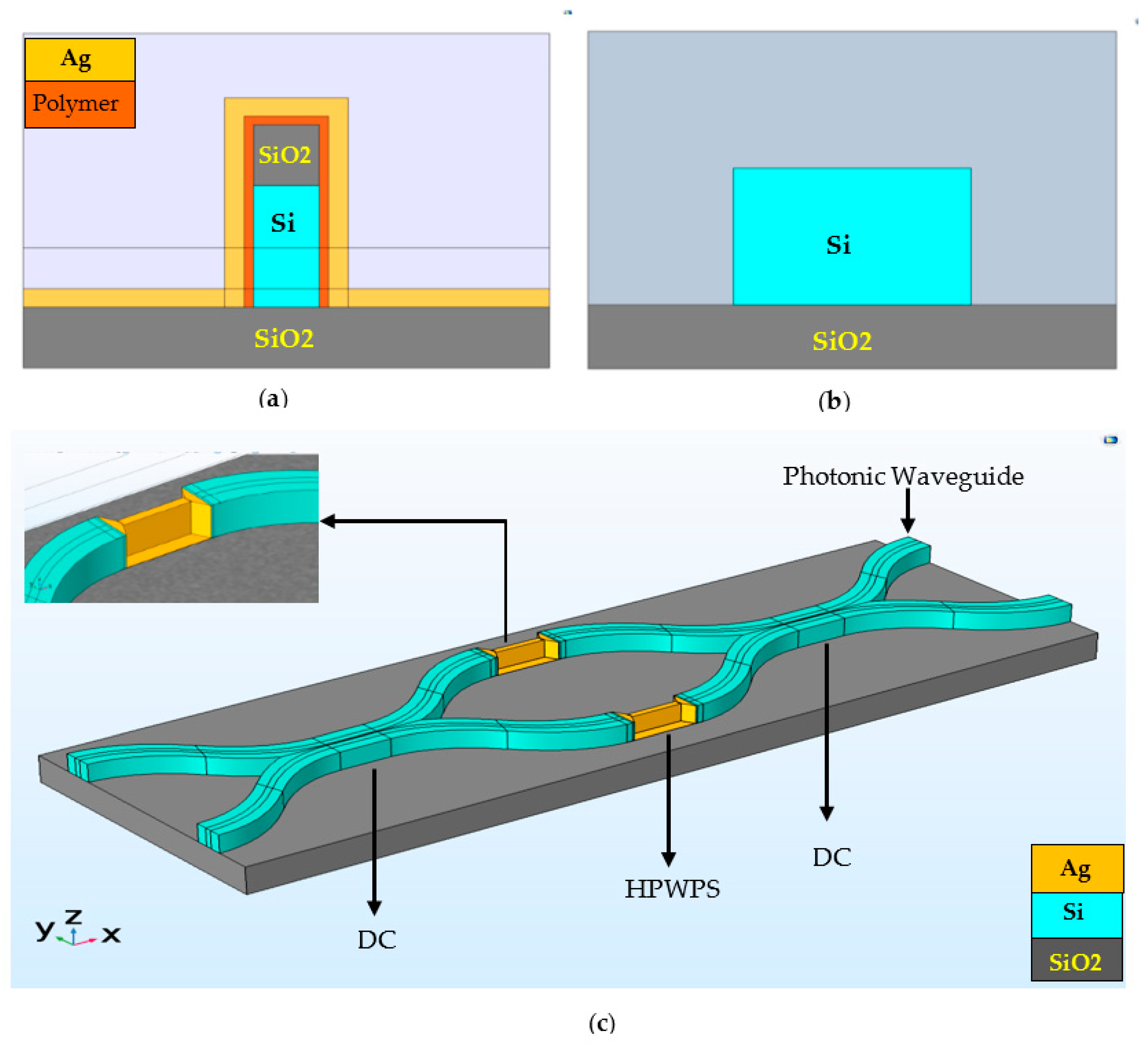
A miniaturized 2 × 2 electro-optic plasmonic MZS has been designed based on a metal-polymer-silicon hybrid waveguide, as shown in Figure 1. The design issues of this switch have been reported in our previous work [41] and only a summary of switch performance characteristics is given here. Adiabatic tapers are designed carefully to efficiently couple the light between the plasmonic phase shifter, implemented in each of the MZS arms, and the 3-dB input/output DCs. For a 6 µm-long hybrid plasmonic waveguide supported by JRD1 polymer ( r 33 = 390 pm/V), a π-phase shift voltage of 2 V is obtained. The switch is designed for 1550 nm operation wavelength using COMSOL software and characterized by 2.3 dB insertion loss, 9.9 fJ/bit power consumption, and 640 GHz electric bandwidth. These results indicate that the designed switch outperforms the nanoplasmonic MZSs reported in the literature and can be used as a basic–switch unit for implementing N × N plasmonic switches. The hybrid plasmonic waveguide phase shifter consists of silicon (Si), silica ( SiO 2 ), polymer (JRD1), and silver (Ag) layers (as shown in Figure 2a) and it extends to the tapers. Figure 2b shows the cross section of the switch photonic waveguide, while a three-dimensional (3D) view of the designed MZS is shown in Figure 2c. The excited surface plasmon waves appear at the sidewall of the metal-polymer interface. As the plasmonic mode is confined to the sidewall of the polymer layer, rather than in the metal/dielectric interface, the top of the waveguide is covered by a thick SiO 2 layer to reduce the absorption loss associated with a plasmonic mode.
The structural parameters and material layer refractive indices used to design the switch for 1550 nm-operation wavelength are listed in Table 1.
JRD1 is chosen as the polymer layer, since it has a high EO coefficient as compared to other polymer materials used in plasmonic waveguides reported in the literature.

3. Scaling to a 4 × 4 Nonblocking Plasmonic Switch

This section presents design issues and characteristics of a 4 × 4 nonblocking optical switch incorporating the designed 2 × 2 hybrid plasmonic MZS as the basic switching cell. The analysis and simulation results can be used as a guideline to design N × N optical switches with N = 2 n and n 3 .

3.1. Switch Model

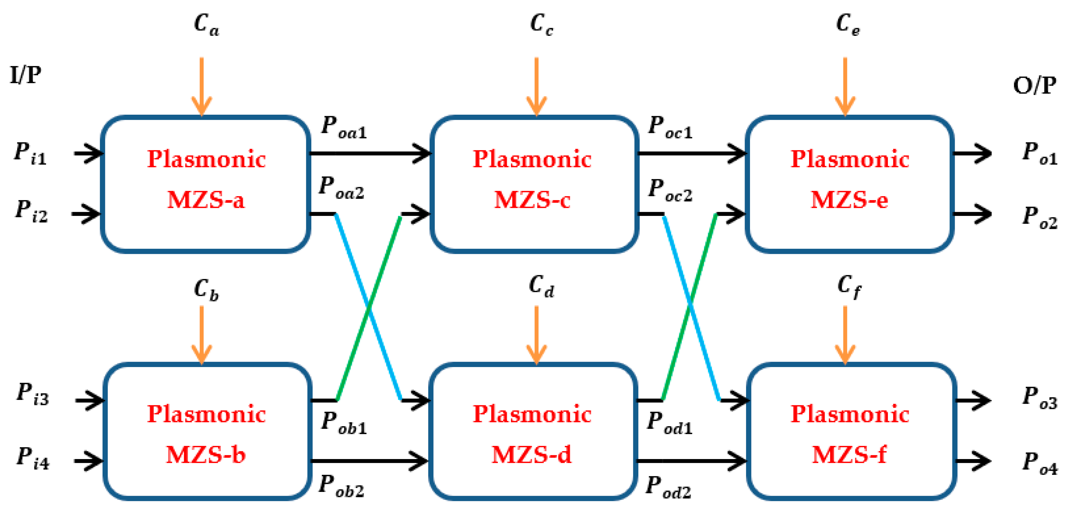
Figure 3 shows a simplified configuration of the 4 × 4 switch under investigation. The switch consists of six 2 × 2 plasmonic MZSs, denoted by MZS-a to MZS-f, which are controlled by six binary signals, C a to C f . Each control signal is applied to one of the six MZSs to control its arm-phase difference, Ø a to Ø f . The phase difference Ø is switched between 0 and π to operate the switch operation in the cross-state or bar-state mode, respectively.
Assuming the six MZSs are identical and designed with identical 3dB-DCs (τ = κ) and equal arm loss, then the 4 × 4 switch is characterised by a 4 × 4 power transfer matrix T b
[ P o 1 P o 2 P o 3 P o 4 ] = T b [ P i 1 P i 2 P i 3 P i 4 ]
The 16 elements of the matrix T b are given by:
t 11 = Q 3   [ sin ( Ø a 2 ) sin ( Ø c 2 ) sin ( Ø e 2 ) ] 2
t 12 = Q 3   [ cos ( Ø a 2 ) sin ( Ø c 2 ) sin ( Ø e 2 ) ] 2
t 13 = Q 3   [ cos ( Ø a 2 ) sin ( Ø c 2 ) sin ( Ø e 2 ) ] 2
t 14 = Q 3   [ cos ( Ø a 2 ) sin ( Ø c 2 ) sin ( Ø e 2 ) ] 2
t 21 = Q 3   [ sin ( Ø a 2 ) sin ( Ø c 2 ) sin ( Ø e 2 ) ] 2
t 22 = Q 3   [ cos ( Ø a 2 ) sin ( Ø c 2 ) sin ( Ø e 2 ) ] 2
t 23 = Q 3   [ cos ( Ø a 2 ) sin ( Ø c 2 ) sin ( Ø e 2 ) ] 2
t 24 = Q 3   [ cos ( Ø a 2 ) sin ( Ø c 2 ) sin ( Ø e 2 ) ] 2
t 31 = Q 3   [ sin ( Ø a 2 ) sin ( Ø c 2 ) sin ( Ø e 2 ) ] 2
t 32 = Q 3   [ cos ( Ø a 2 ) sin ( Ø c 2 ) sin ( Ø e 2 ) ] 2
t 33 = Q 3   [ cos ( Ø a 2 ) sin ( Ø c 2 ) sin ( Ø e 2 ) ] 2
t 34 = Q 3   [ cos ( Ø a 2 ) sin ( Ø c 2 ) sin ( Ø e 2 ) ] 2
t 41 = Q 3   [ sin ( Ø a 2 ) sin ( Ø c 2 ) sin ( Ø e 2 ) ] 2
t 42 = Q 3   [ cos ( Ø a 2 ) sin ( Ø c 2 ) sin ( Ø e 2 ) ] 2
t 43 = Q 3   [ cos ( Ø a 2 ) sin ( Ø c 2 ) sin ( Ø e 2 ) ] 2
t 44 = Q 3   [ cos ( Ø a 2 ) sin ( Ø c 2 ) sin ( Ø e 2 ) ] 2
where Q = [ 4 τ 4 e 2 α L ]
Equation (17a–p) are valid when the phase deference Ø for each switch takes 0 or π and therefore, the mixing between the two inputs of the MZS does not appear at the output. Further, deriving general expressions for the power transfer matrix elements when the six MZS do not have identical characteristics with τ ≠ κ is straightforward and it is not given here owing to space limitations.
Note that signal transition between each of the switch inputs to one of its outputs passes through three MZSs. Each of these three switches operates in a binary state, either in the bar or cross state. The states of the other three switches, which are not involved in the signal transition path, do not affect the switching operation and can be considered in the “do not-care state”. This state is denoted in the binary logic circuits and systems by the letter X to distinguish it from the effective state (0 or 1). According to these remarks, the operation of the 4 × 4 switch covers 24 switching states, as listed in Table 2. Note that 24 = 2 3 × 3 ( 1 ) , where the numbers 2 and 1 refer, respectively, to the binary state and X state.

3.2. Simulated and Calculated Results

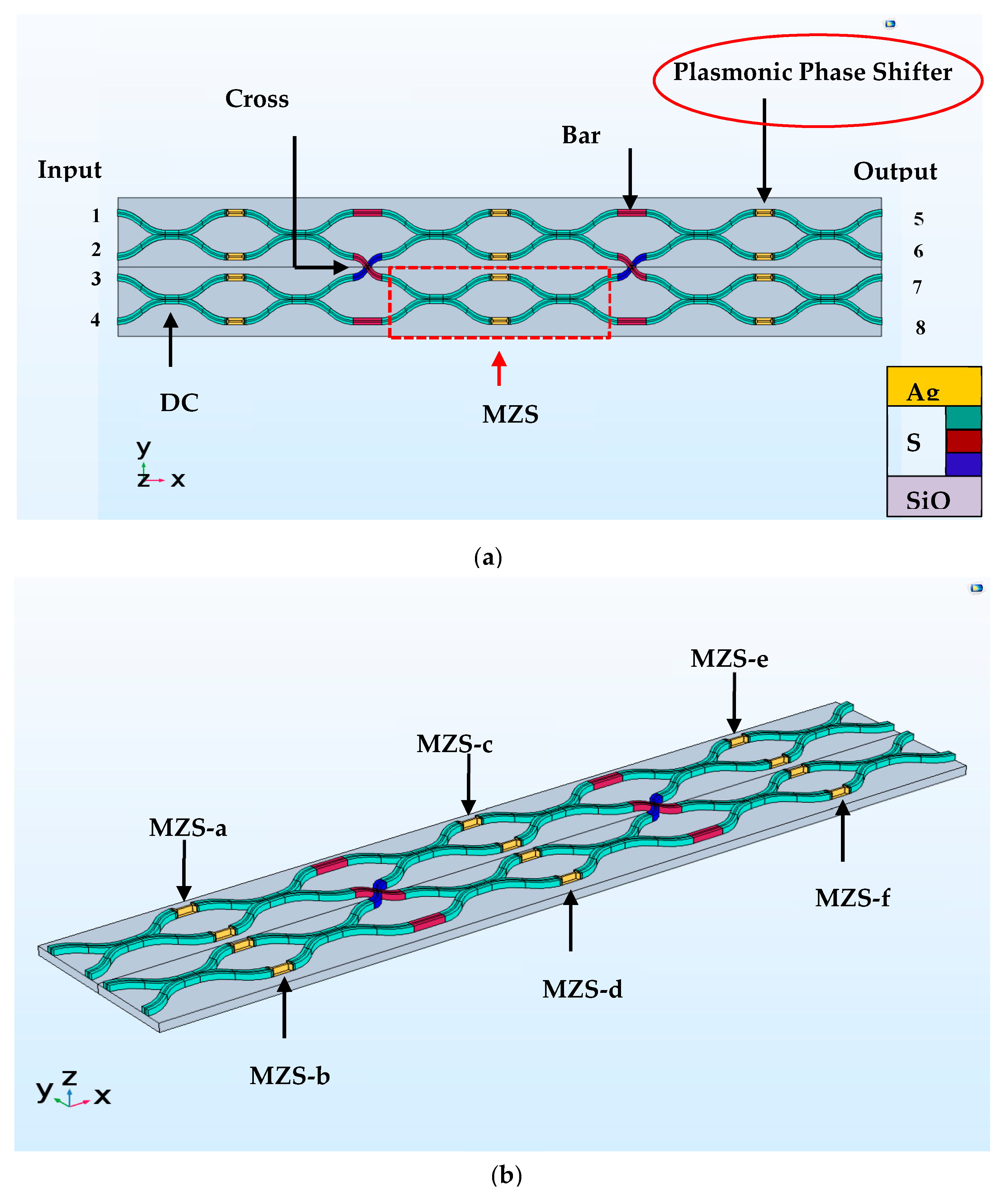
Figure 4 shows 2D and 3D schematic diagrams of the 4 × 4 plasmonic-based optical switch, as presented in the COMSOL environment. The switch is designed for 1550 nm-wavelength operation and has CMOS compatibility. The switch covers 550   µ m × 70   µ m area and uses single-derived MZSs that operate with 0 and 2 V control signals.

3.2.1. Simulated Results

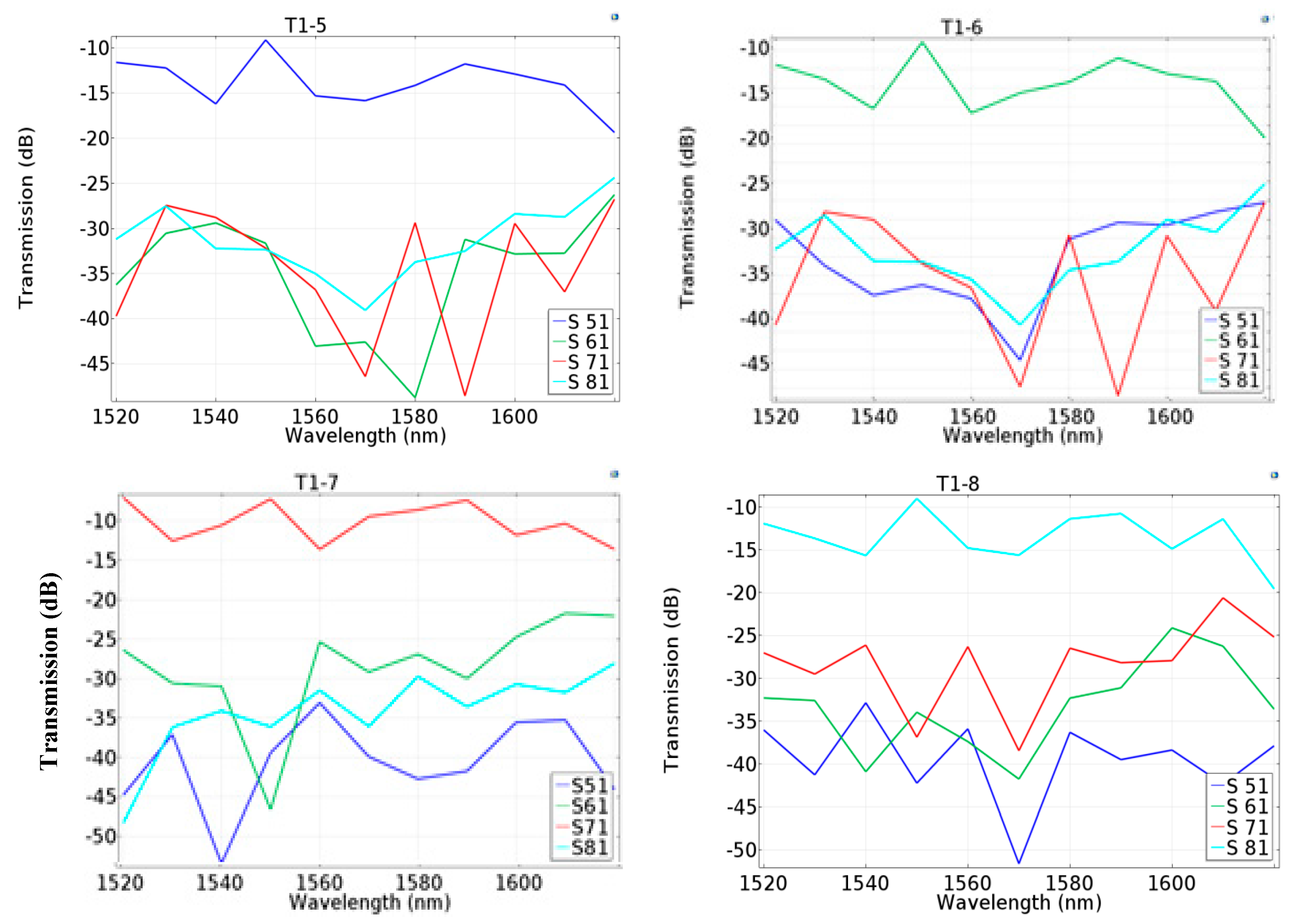
The transmission characteristics of the switch is simulated over 1520–1620 nm signal-wavelength range using COMSOL. The spectra of the scattering parameters (S-parameters) that represent the transmission coefficients from each of the input ports to each of the output ports are recorded. Example of the results corresponding to input port 1 are shown in Figure 5. The switch has four input ports and four output ports. The input ports are labeled by numbers 1–4 to denote inputs 1–4, respectively. The output ports are labeled by numbers 5–8 to denote outputs 1–4, respectively (see Figure 4). Figure 5 contains four plots, each corresponds to the switching state for one of the four output ports describing the related S-parameters. The scattering parameter S i j denote the transmission coefficient from port j (j = 1, 2, 3 and 4) to port i (i = 1, 2, 3 and 4).
Note that S 51 has the highest value compared with S 61 , S 71 , and S 81 which represents the crosstalk in this case under observation. Note that the required transmission coefficient S 51 peaks at the desired wavelength (1550 nm).
The simulation is carried further to record the field distribution at the four output ports when one of the input ports is excited by a signal. A sample of the results is presented in Figure 6 when the signal is applied at input port 1. The figure shows the case when the input signal is switched from input port 1 to output port 6. The results reveal that the field intensity at the required output is much higher than the field intensity at the other three output ports. This demonstrates the capability of the switch to operate with very low crosstalk level at the three non-required output ports.

3.2.2. Calculated Performance Parameters

This subsection presents the crosstalk and loss characteristics of the designed 4 × 4 switch at 1550 nm wavelength. The results are obtained from the scattering parameters depicted in Figure 5.
a. Crosstalk
The crosstalk parameter (CT) of the switch is deduced using the following procedure. An optical signal of certain power (say 0 dBm) is applied only at one of the input ports and then the power at each of the four output ports is recorded. Then the crosstalk is calculated using the following expression:
C T = M a x   ( P o u P o d ) u d u , d = 1 , 2 , 3   and   4 ,
where P o d is the power at the desired output port and P o u is the power at the unwanted port. Using dB measure, Equation (18a) can be rewritten as:
C T d B = M a x   [ P o u ( dBm ) P o d ( dBm ) ] u d u , d = 1 , 2 , 3   and   4 ,
According to Equation (18a,b), the observer looks at the highest power among the undesired ports to estimate the crosstalk corresponding to the switching state under investigation.
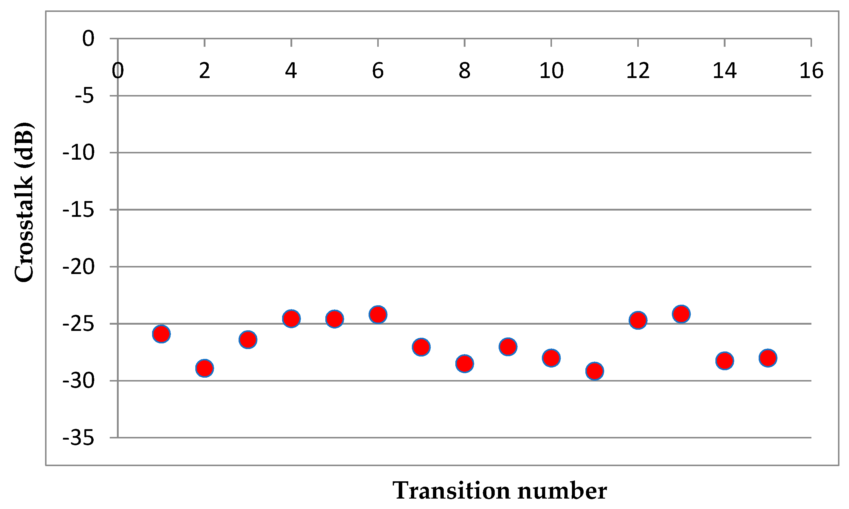
Table 3 lists the crosstalk associated with each of the 16 required transitions corresponding to the switching from one of the four input ports to one of the four output ports. Numbers 1–16 are used to distinguish these transition states, as shown in Table 3.
Figure 7 displays the CT as a function of the transition number. The crosstalk is characterized by −26.5 dB average and 1.9 dB standard deviation.
b. Losses
One of the main performance parameters of the optical switch is the loss along the desired transition path. This path connects one of the input ports, at which the signal is applied, to the desired output port. The path loss in dB between an input port to an output port can be calculated as L p d ( dB ) = P i p ( dBm ) P o d ( dBm ) where p and d = 1, 2, 3 and 4. This loss measure concept gives 16 values corresponding to the 16 desired transitions. Table 2 gives the desired output power for each of the 16 transitions (highlighted by green color) when the input power is 0 dBm. Therefore, the transition path loss can be deduced form this table as L p d ( dB ) = P o d   ( dBm ) | P i p = 0 dBm . The average and standard deviation of the transition path loss are found to be 7.4 dB and 0.25 dB, respectively.
It is worth mentioning here that the six 2 × 2 MZSs used to design the 4 × 4 optical switch have identical structures. Therefore, it is expected that their cross losses (and bar losses) should also be identical. To check this point, the cross and bar losses for each of the six elementary MZSs used in the COMSOL-environment design of the 4 × 4 switch are deduced from the simulation. The results are given in Table 4.

3.2.3. Performance Comparison with Related Published Works

Table 5 compares the performance parameters of the proposed switch with those of the conventional (nonplasmonic) switches reported in the published literature. The four switches in this table reflect common characteristics where each of them is a 4 × 4 nonblocking switching configuration designed on a silicon photonic platform using a matrix of MZSs. One of the performance parameters in this table is the power consumption required to change the phase difference of each of the three 2 × 2 MZSs involved in the transition switching path by π radian. This parameter estimates the maximum power consumption occurring during the switching operation. The 2 × 2 MZS used in our proposed switch consumes 9.9 fJ/bit according to the investigation reported in Ref. [41]. Assuming a 100 Gbps operation, the proposed switch consumes 3 × 9.9 × 10−5 × 100 × 109 ≅ 3 mW.
An investigation of the results in Table 5 reveals that:
(i)
The proposed switch has the smallest area, which equals 1/127, 1/390, and 1/12.5 of the area of the switches reported in Refs. [8,47,48], respectively.
(ii)
The proposed switch consumes the lowest power. The other three switches consume about 11, 8, and 7 times the power consumed by the proposed switch, respectively.
(iii)
The proposed switch has the lowest V π L parameter, which is about 1/21 and 1/18 of that of the switches reported in the Ref. [47,48], respectively.
(iv)
The proposed switch has an insertion loss almost to that of Ref. [8], but higher than those reported in Ref. [47,48] by 4.7 and 1.9, respectively.
(v)
The proposed switch is characterized by the lowest crosstalk. The crosstalk of our switch almost matches that of Ref. [47], but outperforms those in Ref. [8,48] by −14.5 and −17.5 dB, respectively.

4. Using the Designed Plasmonic Switch in Optical Networks: Case Study

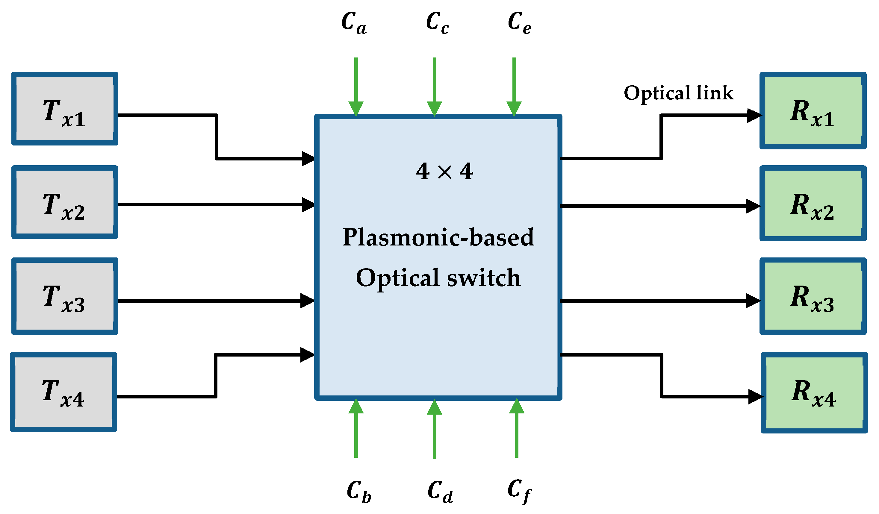
The aim of this section is to investigate the performance of the designed 4 × 4 switch when used as an optical node (or optical router) in optical networks; see Figure 8. Four advanced optical communication transmitters— T x 1 , T x 2 , T x 3 and T x 4 —are connected to the four switch inputs. Each one of the four switch outputs is connected to a multispan optical link to deliver the signal to one of the four receivers R x 1 , R x 2 , R x 3 , and R x 4 . The optical network under investigation is implemented using Optisystem software ver. 14.1 to cover two cases. The first case, wavelength-division-multiplexing (WDM) communication system, is transmitted over each optical link. Each of the four WDM transmitters (and hence each of the four WDM receivers) deals with a C-band multichannel system (C-band covers 1530–1565 nm wavelength). In the second case, the routing ability of the designed 4 × 4 switch is addressed.
The designed 4 × 4 switch is implemented in the Optisystem environment using six 2 × 2 MZSs. A library element is designed for the plasmonic MZS in the Optisystem software, which takes into account its structure and performance parameters. Among these parameters are coupling coefficient and loss of the input and output directional couplers, losses of the upper and lower arms of the MZS, and extinction ratios E R b a r   and   E R c r o s s corresponding to bar and cross states, respectively. These extinction ratios are reflected in the design by modifying the phase shift ∆Ø between the two MZS arms.
Ø = { 2 tan 1 E R b a r Bar   state 2 cot 1 E R c r o s s Cross   state ,
Equation (19) is deduced by noting that in the cross or bar state, one of the 2 × 2 switch output delivers sin 2 ( Ø / 2 ) power component, while the other port delivers cos 2 ( Ø / 2 ) power component.
It is worth mentioning here that in a high speed switching operation, the electrical bandwidth of the MZS plays a key role in determining the switching performance. This effect is included in the designed MZS-library element by passing the control signal through a low pass filter before applying it to the switch. The filter bandwidth matches the electrical switch bandwidth.

4.1. Case I: WDM Transmission

This case addresses the possibility of using the desired 4 × 4 switch to route WDM signals. Four WDM transmitters ( T x 1 , T x 2 , T x 3 , and T x 4 ) are connected to the four inputs of the switch. Each one of the switch output is connected to one of four WDM receivers ( R x 1 , R x 2 , R x 3 , and R x 4 ) through a multispan optical link. The WDM transmitter has an 8-channel system (with each channel carrying 40 Gbps nonreturn-to-zero (NRZ) signals) and 4 dBm-power semiconductor lasers. The frequencies of these lasers extend from 192.8 THz (1st laser) to 193.5 THz (8th laser). The fourth channel (193.1 THz, which corresponds to 1550 nm) is taken as the center channel. Each span of the optical link consists of 50 km SSMF ( α = 0.2 dB/km, D = 17 ps/(nm⋅km), and S = 0.075 ps/( nm 2 ⋅km)) followed by a 10 km dispersion-compensated fiber (DCF) having α = 0.5 dB/km, D = 85 ps/(nm⋅km), and S = 0.3 ps/( nm 2 ⋅km). 10 dB and 5 dB OAs are inserted after the SSMF and DCF sections, respectively, to compensate for the fiber loss. The WDM receiver uses a demultiplexer to split the received WDM waveform into eight channels using 80 GHz-bandwidth optical bandpass filters. Each of the eight outputs of the WDM multiplexer is applied to a direct detection optical receiver to recover the transmitted data associated with that channel.
Few remarks related to the used 4 × 4 plasmonic-based optical switch should be noted before simulating the WDM optical network under observation.
(i)
The optical bandwidth B o p t of the 2 × 2 MZS is assumed to be dominated by the photon transit time τ t r across the MZS. Thus, ( B o p t ) 2 × 2 = 1 / 2 π ( n e f f ) r τ t r = c / ( n e f f ) r L where c is the speed of the light in vacuum, L is the MZS arm length, and ( n e f f ) r is the real part of the effective refractive index of the propagating mode in the MZS arm. The 2 × 2 switch is designed here with L = 6 µm and has ( n e f f ) r = 2.69 . These values yield ( B o p t ) 2 × 2 = 3 THz. This limited optical bandwidth has been taken into account when the 2 × 2 MZS is designed as a library element in the Optisystem software. A second-order optical Gaussian bandpass filter with 3 THz bandwidth centered at 1550 nm wavelength is inserted at each of the two switch inputs.
(ii)
The transmission path between one of the switch inputs and one of its output ports consists of three cascaded 2 × 2 MZS. According to electrical filter theory, cascading in identical filter stages yields a higher-order filter whose bandwidth equals 2 1 / n 1 of the single-stage bandwidth. According to this concept, the optical bandwidth of the 4 × 4 switch, ( B o p t ) 4 × 4 equals 2 1 / 3 1 ( B o p t ) 2 × 2 ≅ 0.5 × 3 = 1.5 THz. Note that the optical bandwidth of the designed 4 × 4 switch is higher than the bandwidth of the 8 × 40 Gbps WDM signal (≅8 × 40 = 320 GHz).
(iii)
The 2 × 2 MZS is designed to operate at 1550 nm wavelength, which is almost the center of the 8-channel WDM spectrum. Thus, the maximum frequency deviation DF from the center frequency equals to 320/2 = 160 GHz, which corresponds to the lower (or upper) edge of the WDM spectrum. This frequency deviation, which yields a change δ Ø in the bar-state phase shift difference, equals 180 ° Df/ f c e n t e r = 0.15°, where f c e n t e r is the center frequency corresponding to λ = 1550 nm. Therefore δ Ø / 180 ° = 8.3 × 10 4 and hence the MZS can be treated to operate with ∆Ø = 180° in the bar state (and 0° in the cross state) over the whole WDM signal spectrum. This will simplify the simulation, since ∆Ø is not modified with each spectrum component and is fixed at 0 ° or 180° according to the operating state.
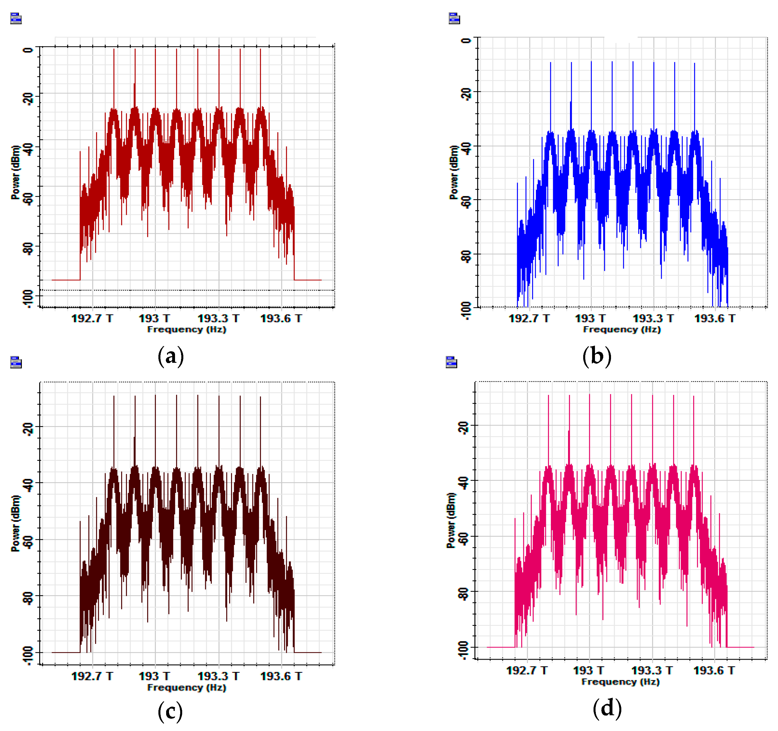
The 4 × 4 switch-based WDM optical network is simulated using the Optisystem software, where the switch is controlled to route T x 1 to R x 4 . Figure 9 shows the optical spectra at different points of the network. Parts a-c of this figure illustrate the spectra at the output of T x 1 , fourth output port of the switch, and input of the receiver R x 4 after 13-span transmission link, respectively. Part d of this figure displays the received optical spectrum at R x 4 when the effect of fiber nonlinear optics of the 13-span link is turned off in the used software. The results in Figure 9 highlight the following facts:
(i)
The optical switch is able to route the WDM signal from the input to the output without altering its frequency contents. This result is expected since the bandwidth of the WDM signal equals approximately 20% (≅320 GHz/1500 GHz) of the switch optical bandwidth.
(ii)
The spectrum level is reduced by 7.7 dB when the signal is routed from first input port to the fourth output port.
(iii)
The effect of fiber nonlinear optics is almost negligible, which makes the spectrum at the fiber output match that of the fiber input. This conclusion is confirmed further by noting that the spectrum at the fiber output does not change when the effect of fiber nonlinear optics is turned off in the software.
It is worth discussing here why the effect of fiber nonlinear optics is negligible in the simulated network. Each of the eight transmitters in the WDM system uses 4 dBm-semiconductor lasers. If the NRZ signaling contains an equal number of zeros (OFF states) and ones (ON states), then the average power at each channel transmitter equals half the laser power ( 4 + 10 log 0.5 = 1 dBm). The optical power of the WDM transmitter = 1 + 10 log 8 = 10 dBm.
The power of the WDM signal at the switch output that is launched into the fiber = 10 7.7 = 2.3 dBm. This power level is relatively low and cannot enhance the fiber nonlinearity optics.
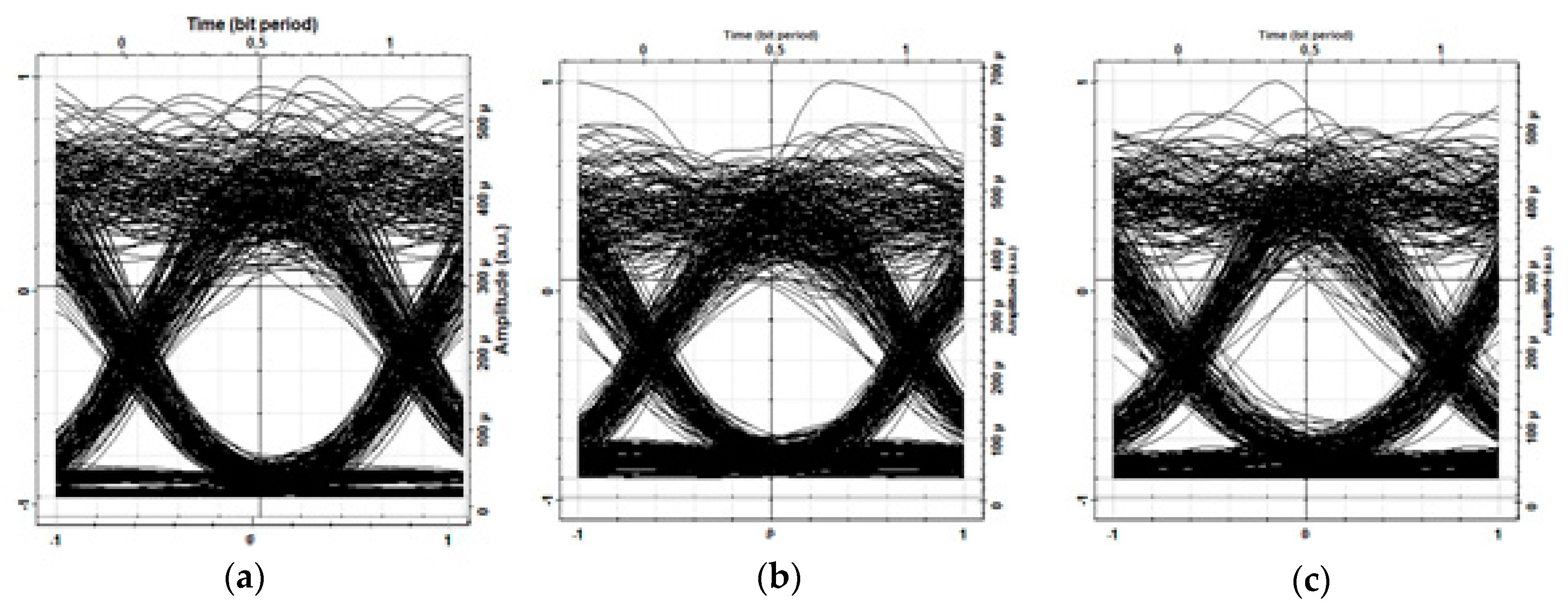
The eye diagrams of the WDM channels are recorded in R x 4 after 13-span transmission. Sample of results related to Channel 1, Channel 4, and Channel 8 are given in Figure 10 which give BERs of 3.0 × 10 12 , 1.2 × 10 11 , and 6.9 × 10 12 , respectively. Increasing the number of link spans to 4 gives BERs of 5.2 × 10 11 , 9.0 × 10 13 , and 2.9 × 10 9 , respectively. Note that in this case, Ch8 has a BER > 10 9 which is usually used as a threshold BER in WDM network.

4.2. Case II: Multi-Input Multi-Output Operation

The aim of this test is to address the ability of the designed 4 × 4 switch to route the four input signals simultaneously to the output ports. In this test, four WDM transmitters are connected to the four input of the switch.
  • T x 1 : 4 × 40 Gbps NRZ (lasers frequencies span from 193.0–193.3 THz).
  • T x 2 : Similar to T x 1 but with return-to-zero (RZ) signaling.
  • T x 3 : 8 × 40 Gbps NRZ (lasers frequencies span from 192.8–193.5 THz).
  • T x 4 : Similar to T x 3 but with return-to-zero (RZ) signaling.
All the six control logics are set to zero to ensure that all the switches operate at cross state. Under this condition, input 1, 2, 3, and 4 are switched to outputs 3, 4, 1, and 2, respectively. This is illustrated in Figure 11, which displays the optical spectrum at the input and output ports. Note that the switch is able to route the four inputs successfully to four outputs with conserved spectrum frequency contents. Such results are expected, since each arm of the six 2 × 2 MZSs used in the design of the 4 × 4 switch deals only with one of the input signals and is not affected by the others. To illustrate this point, the following notations are used in the following discussion. The bar and cross states corresponding to input i (i = 1 and 2 ) of switch “a” are denoted by a i and a i ¯ , respectively. Simillar notations are used for other five switches (switch “b” to switch “f”). When all the six control logics are zero, the following four paths are used:
  • a ¯ 1   d ¯ 1 f ¯ 2    From input 1 to output 3
  • a ¯ 2   c ¯ 1 f ¯ 1    From input 2 to output 4
  • b ¯ 1   d ¯ 2 e ¯ 2    From input 3 to output 1
  • b ¯ 2   c ¯ 2 e ¯ 1    From input 4 to output 2
Note that no arm path is common between two (or more) transitions.

5. Conclusions

A plasmonic-based 4 × 4 nonblocking switch has been successfully designed and investigated using COMSOL software. The switch has six 2 × 2 plasmonic MZSs with a total footprint of ( 500 × 70   µ m 2 ). The switch operates at 1550 nm with an optical bandwidth of 1.5 THz, V π L = 12   V · µ m , maximum insertion loss of 7.7 dB, and −26.5 dB crosstalk. These results outperform those reported in the literature using conventional (nonplasmonic) counterparts. The switch has been tested as a router in optical networks using Optisystem software, where two cases have been investigated successfully. The first case deals with routing one of four 8 × 40 Gbps WDM signals and transmit resultant switch output signal over 650 km over SSMF. These results confirm the successful switching function of the proposed switch, even for WDM input signals having 320 Gbps data rate. The second case has tested the designed 4 × 4 switch to simultaneously route signals from input ports to the output ports. The obtained results show the successful routing ability of the proposed switch. Future studies will be conducted in the future to cover the effect of temperature variation and fabrication error on the performance of the proposed 4 × 4 switch.

Author Contributions

Conceptualization, R.S.F. and S.K.T.; Methodology, R.S.F.; Software, M.S.J.; Validation, M.S.J., S.K.T. and R.S.F.; Formal Analysis, M.S.J.; Investigation, M.S.J.; Resources, M.S.J.; Data Curation, M.S.J.; Writing-Original Draft Preparation, R.S.F. and S.K.T.; Writing-Review & Editing, R.S.F. and S.K.T.; Visualization, M.S.J.; Supervision, S.K.T.; Project Administration, S.K.T.

Funding

This research received no external funding.

Conflicts of Interest

The authors declare no conflict of interest.

References

  1. Chen, K.; Duan, F.; Yu, Y. Performance-enhanced silicon thermo-optic Mach–Zehnder switch using laterally supported suspended phase arms and efficient electrodes. Opt. Lett. 2019, 44, 951–954. [Google Scholar] [CrossRef]
  2. Fan, G.; Orobtchouk, R.; Han, B.; Li, Y.; Li, H. 8 × 8 wavelength router of optical network on chip. Opt. Express 2017, 25, 23677–23683. [Google Scholar] [CrossRef] [PubMed]
  3. Guo, P.; Hou, W.; Guo, L.; Yang, Q.; Ge, Y.; Liang, H. Low Insertion Loss and Non-Blocking Microring-Based Optical Router for 3D Optical Network-on-Chip. IEEE Photonics J. 2018, 10. [Google Scholar] [CrossRef]
  4. Annoni, A.; Guglielmi, E.; Carminati, M.; Grillanda, S.; Ciccarella, P.; Ferrari, G.; Sorel, M.; Strain, M.J.; Sampietro, M.; Melloni, A.; et al. Automated Routing and Control of Silicon Photonic Switch Fabrics. IEEE J. Sel. Top. Quantum Electron. 2016, 22, 169–176. [Google Scholar] [CrossRef] [Green Version]
  5. Chen, C.P.; Zhu, X.; Liu, Y.; Wen, K.; Chik, M.S.; Baehr-Jones, T.; Hochberg, M.; Bergman, K. Programmable Dynamically-Controlled Silicon Photonic Switch Fabric. IEEE J. Lightwave Technol. 2016, 34, 2952–2958. [Google Scholar] [CrossRef]
  6. Mendez, M.; Okamoto, M.; Ito, Y.; Kita, T. Compact thermo-optic MZI switch in siliconon-insulator using direct carrier injection. Opt. Express 2019, 27, 899–906. [Google Scholar] [CrossRef] [PubMed]
  7. Rizal, C.S.; Niraula, B. Compact Si-based asymmetric MZI waveguide on SOI as a thermo-optical switch. Opt. Commun. 2017, 410, 947–955. [Google Scholar] [CrossRef]
  8. Lu, L.; Zhou, L.; Li, Z.; Li, X.; Chen, J. Broadband 4 × 4 Nonblocking Silicon Electrooptic Switches Based on Mach–Zehnder Interferometers. IEEE Photonics J. 2015, 7. [Google Scholar] [CrossRef]
  9. Lee, B.G.; Rylyakov, A.V.; Green, W.M.; Assefa, S.; Baks, C.W.; Rimolo-Donadio, R.; Kuchta, D.M.; Khater, M.H.; Barwicz, T.; Reinholm, C.; et al. Monolithic Silicon Integration of Scaled Photonic Switch Fabrics, CMOS Logic, and Device Driver Circuits. IEEE J. Lightwave Technol. 2014, 32, 743–751. [Google Scholar] [CrossRef]
  10. Soref, R. Design of low-energy on-chip electro-optical 1 × M wavelength-selective switches. Photonics Res. 2017, 5, 340–345. [Google Scholar] [CrossRef]
  11. Dupuis, N.; Lee, B.G. Impact of Topology on the Scalability of Mach–Zehnder-Based Multistage Silicon Photonic Switch Networks. IEEE J. Lightwave Technol. 2018, 36, 763–772. [Google Scholar] [CrossRef]
  12. Qiao, L.; Tang, W.; Chu, T. 32 × 32 silicon electro-optic switch with built-in monitors and balanced-status units. Sci. Rep. 2017, 7, 42306. [Google Scholar] [CrossRef] [Green Version]
  13. Jia, H.; Zhou, T.; Zhao, Y.; Xia, Y.; Dai, J.; Zhang, L.; Ding, J.; Fu, X.; Yang, L. Six-port optical switch for cluster-mesh photonic network-on-chip. Nanophotonics 2018, 7, 827–835. [Google Scholar] [CrossRef] [Green Version]
  14. Soref, R. Tutorial: Integrated-photonic switching structures. Am. Inst. Phys. 2018, 3. [Google Scholar] [CrossRef]
  15. Lee, B.G.; Dupuis, N. Silicon Photonic Switch Fabrics: Technology and Architecture. IEEE J. Lightwave Technol. 2019, 37, 6–20. [Google Scholar] [CrossRef]
  16. Sun, X.; Zhou, L.; Li, X.; Hong, Z.; Chen, J. Design and analysis of a phase modulator based on a metal–polymer–silicon hybrid plasmonic waveguide. Appl. Opt. 2011, 50, 3428–3434. [Google Scholar] [CrossRef]
  17. Tsareva, A.; Tazieva, R.; Hellerc, E.; Chalonyd, M. Polymer electro-optic modulator efficiency enhancement by the high permittivity dielectric strips. Photonics Nanostruct. Fundam. Appl. 2017. [Google Scholar] [CrossRef]
  18. Zhang, Y.; Ling, Y.; Zhang, Y.; Shang, K.; Yoo, S.B. High-Density Wafer-Scale 3-D Silicon-Photonic Integrated Circuits. IEEE J. Sel. Top. Quantum Electron. 2018, 24. [Google Scholar] [CrossRef]
  19. Kish, F.; Lal, V.; Evans, P.; Corzine, S.W.; Ziari, M.; Butrie, T.; Reffle, M.; Tsai, H.; Dentai, A.; Pleumeekers, J.; et al. System-on-Chip Photonic Integrated Circuits. IEEE J. Sel. Top. Quantum Electron. 2018, 24. [Google Scholar] [CrossRef]
  20. Minkenberg, C.; Farrington, N.; Zilkie, A.; Nelson, D.; Lai, C.P.; Brunina, D.; Byrd, J.; Chowdhuri, B.; Kucharewski, N.; Muth, K.; et al. Reimagining Datacenter Topologies with Integrated Silicon Photonics. J. Opt. Commun. Netw. Opt. Soc. Am. 2018, 10, 126–139. [Google Scholar] [CrossRef]
  21. Tanaka, S.; Simoyama, T.; Aoki, T.; Mori, T.; Sekiguchi, S.; Jeong, S.; Usuki, T.; Tanaka, Y.; Morito, K. Ultralow-Power (1.59 mW/Gbps), 56-Gbps PAM4 Operation of Si Photonic Transmitter Integrating Segmented PIN Mach–Zehnder Modulator and 28-nm CMOS Driver. IEEE J. Lightwave Technol. 2018, 36, 1275–1280. [Google Scholar] [CrossRef]
  22. Dabos, G.; Manolis, A.; Papaionnou, S.; Tsiokos, D.; Markey, L.; Weeber, J.-C.; Dereux, A.; Giesecke, A.L.; Porschatis, C.; Chmielak, B.; et al. CMOS plasmonics in WDM data transmission: 200 Gb/s (8 × 25Gb/s) transmission over aluminum plasmonic waveguides. Opt. Express 2018, 26, 12469–12478. [Google Scholar] [CrossRef] [PubMed]
  23. Heni, W.; Hoessbacher, C.; Haffner, C.; Fedoryshyn, Y.; Baeuerle, B.; Josten, A.; Hillerkuss, D.; Salamin, Y.; Bonjour, R.; Melikyan, A.; et al. High speed plasmonic modulator array enabling dense optical interconnect solutions. Opt. Express 2015, 23, 29746–29757. [Google Scholar] [CrossRef] [PubMed] [Green Version]
  24. Ozbay, E. Plasmonics: Merging Photonics and Electronics at Nanoscale Dimensions. Science 2006, 311, 189–193. [Google Scholar] [CrossRef] [PubMed] [Green Version]
  25. Song, J.; Tian, Y.; Ye, S.; Chen, L.; Peng, X.; Qu, J. Characteristic Analysis of Low-Threshold Plasmonic Lasers Using Ag Nanoparticles with Various Shapes Using Photochemical Synthesis. IEEE J. Lightwave Technol. 2015, 33, 3215–3223. [Google Scholar] [CrossRef]
  26. Rahman, M.Z.; Krishna, K.M.; Reddy, K.K.; Babu, M.V.; Mirza, S.S.; Fathima, S.Y. Ultra-Wide-Band Band-Pass Filters Using Plasmonic MIM Waveguide-Based Ring Resonators. IEEE Photonics Technol. Lett. 2018, 30, 1715–1718. [Google Scholar] [CrossRef]
  27. Dorodnyy, A.; Salamin, Y.; Ma, P.; Plestina, J.V.; Lassaline, N.; Mikulik, D.; Romero-Gomez, P.; Morral, A.F.; Leuthold, J. Plasmonic Photodetectors. IEEE J. Sel. Top. Quantum Electron. 2018, 24, 1–13. [Google Scholar] [CrossRef]
  28. Tomadin, A.; Polini, M. Theory of the plasma-wave photoresponse of a gated graphene sheet. Phys. Rev. B 2013, 88, 205426. [Google Scholar] [CrossRef]
  29. Viti, L.; Coquillat, D.; Politano, A.; Kokh, K.A.; Aliev, Z.S.; Babanly, M.B.; Tereshchenko, O.E.; Knap, W.; Chulkov, E.V.; Vitiello, M.S. Plasma-Wave Terahertz Detection Mediated by Topological Insulators Surface States. Nano Lett. 2016, 16, 80–87. [Google Scholar] [CrossRef] [PubMed]
  30. Koch, U.; Messner, A.; Hoessbacher, C.; Heni, W.; Josten, A.; Baeuerle, B.; Ayata, M.; Fedoryshyn, Y.; Elder, D.L.; Dalton, L.R.; et al. Ultra-Compact Terabit Plasmonic Modulator Array. IEEE J. Lightwave Technol. 2019, 37, 1484–1491. [Google Scholar] [CrossRef]
  31. Baeuerle, B.; Heni, W.; Hoessbacher, C.; Fedoryshyn, Y.; Josten, A.; Haffner, C.; Watanabe, T.; Uhl, C.; Hettrich, H.; Elder, D.L.; et al. Reduced Equalization Needs of 100 GHz Bandwidth Plasmonic Modulators. IEEE J. Lightwave Technol. 2019, 37, 2050–2057. [Google Scholar] [CrossRef]
  32. Wu, H.; Huang, Y.; Shen, P.; Lee, H.; Oketani, R.; Yonemaru, Y.; Yamanaka, M.; Shoji, S.; Lin, K.; Chang, C.; et al. Ultrasmall all-optical plasmonic switch and its application to superresolution imaging. Sci. Rep. 2016. [Google Scholar] [CrossRef] [PubMed]
  33. Singh, M.; Datta, A. Modeling of a Vertical Hybrid Plasmonic Switch with VO2 Fin Bragg Grating. IEEE Photonics Technol. Lett. 2018, 30, 997–1000. [Google Scholar] [CrossRef]
  34. Xiao, J.; Wei, Q.; Yang, D.; Zhang, P.; He, N.; Zhang, G.; Ren, T.; Chen, X. A CMOS-Compatible Hybrid Plasmonic Slot Waveguide with Enhanced Field Confinement. IEEE Electron. Device Lett. 2016, 37, 456–458. [Google Scholar] [CrossRef]
  35. Huong, N.T.; Chinh, N.V.; Hoang, C.M. Wedge Surface Plasmon Polariton Waveguides Based on Wet-Bulk Micromachining. Photonics 2019, 6, 21. [Google Scholar] [CrossRef]
  36. Haffner, C.; Heni, W.; Fedoryshyn, Y.; Josten, A.; Baeuerle, B.; Hoessbacher, C.; Salamin, Y.; Koch, U.; Dordevic, N.; Mousel, P.; et al. Plasmonic Organic Hybrid Modulators—Scaling Highest Speed Photonics to the Microscale. Proc. IEEE 2016, 104, 2362–2379. [Google Scholar] [CrossRef]
  37. Hoessbacher, C.; Josten, A.; Baeuerle, B.; Fedoryshyn, Y.; Hettrich, H.; Salamin, Y.; Heni, W.; Haffner, C.; Kaiser, C.; Schmid, R.; et al. Plasmonic modulator with >170 GHz bandwidth demonstrated at 100 GBd NRZ. Opt. Express 2017, 25, 1762–1768. [Google Scholar] [CrossRef] [PubMed]
  38. Heni, W.; Haffner, C.; Elder, D.L.; Tillack, A.F.; Fedoryshyn, Y.; Cottier, R.; Salamin, Y.; Hoessbacher, C.; Koch, U.; Cheng, B.; et al. Nonlinearities of organic electro-optic materials in nanoscale slots and implications for the optimum modulator design. Opt. Express 2017, 25, 2627–2653. [Google Scholar] [CrossRef] [PubMed]
  39. Pitilakis, A.; Kriezis, E.E. Longitudinal 2 × 2 Switching Configurations Based on Thermo-Optically Addressed Dielectric-Loaded Plasmonic Waveguides. IEEE J. Lightwave Technol. 2011, 29, 2636–2646. [Google Scholar] [CrossRef]
  40. Papaioannou, S.; Giannoulis, G.; Vyrsokinos, K.; Leroy, F.; Zacharatos, F.; Markey, L.; Weeber, J.; Dereux, A.; Bozhevolnyi, S.I.; Prinzen, A.; et al. Ultracompact and Low-Power Plasmonic MZI Switch Using Cyclomer Loading. IEEE Photonics Technol. Lett. 2015, 27, 963–966. [Google Scholar] [CrossRef]
  41. Jaber, M.S.; Tawfeeq, S.K.; Fyath, R.S. Design Investigation of 2 × 2 Mach-Zehnder Optical Switch Based on a Metal-Polymer-Silicon Hybrid Plasmonic Waveguide. Fiber Integr. Opt. 2019, 38, 21–42. [Google Scholar] [CrossRef]
  42. Sun, S.; Narayana, V.K.; Sarpkaya, I.; Crandall, J.; Soref, R.A.; Dalir, H.; El-Ghazawi, T.; Sorger, V.J. Hybrid Photonic-Plasmonic Nonblocking Broadband 5 × 5 Router for Optical Networks. IEEE Photonics J. 2018, 10, 1–13. [Google Scholar] [CrossRef]
  43. Papaioannou, S.; Vyrsokinos, K.; Kalavrouziotis, D.; Giannoulis, G.; Apostolopoulos, D.; Avramopoulos, H.; Zacharatos, F.; Hassan, K.; Weeber, J.; Markey, L.; et al. Merging Plasmonics and Silicon Photonics towards Greener and Faster “Network-on-Chip” Solutions for Data Centers and High-Performance Computing Systems. Semant. Sch. 2012. [Google Scholar] [CrossRef]
  44. Sun, S.; Narayana, V.K.; El-Ghazawi, T.; Sorger, V.J. High Performance Photonic-Plasmonic Optical Router: A Non-blocking WDM Routing Device for Optical Networks. Opt. Soc. Am. 2017. [Google Scholar] [CrossRef]
  45. Ge, Z.; Zhang, L.; Wang, G.; Zhang, W.; Liu, M.; Li, S.; Wang, L.; Sun, Q.; Ren, W.; Si, J.; et al. On-Chip Router Elements Based on Silicon Hybrid Plasmonic Waveguide. IEEE Photonics Technol. Lett. 2017, 29, 952–955. [Google Scholar] [CrossRef]
  46. Dupuis, N.; Rylyakov, A.V.; Schow, C.L.; Kuchta, D.M.; Baks, C.W.; Orcutt, J.S.; Gill, D.M.; Green, W.M.; Lee, B.G. Nanosecond-Scale Mach–Zehnder-Based CMOS Photonic Switch Fabrics. IEEE J. Lightwave Technol. 2017, 35, 615–623. [Google Scholar] [CrossRef]
  47. Dupuis, N.; Lee, B.G.; Rylyakov, A.V.; Kuchta, D.M.; Baks, C.W.; Orcutt, J.S.; Gill, D.M.; Green, W.M.; Schow, C.L. Modeling and Characterization of a Nonblocking 4 × 4 Mach–Zehnder Silicon Photonic Switch Fabric. IEEE J. Lightwave Technol. 2015, 33, 4329–4337. [Google Scholar] [CrossRef]
  48. Yang, M.; Green, W.M.; Assefa, S.; Van Campenhout, J.; Lee, B.G.; Jahnes, C.V.; Doany, F.E.; Schow, C.L.; Kash, J.A.; Vlasov, Y.A. Non-Blocking 4 × 4 Electro-Optic Silicon Switch for On-Chip Photonic Networks. Opt. Express 2011, 19, 47–54. [Google Scholar] [CrossRef]
  49. Luan, J.; Fan, M.; Zheng, P.; Yang, H.; Hu, G.; Yun, B.; Cui, Y. Design and Optimization of a Graphene Modulator Based on Hybrid Plasmonic Waveguide with Double Low-Index Slots. Plasmonics 2019, 14, 133–138. [Google Scholar] [CrossRef]
  50. Optiwave Systems Inc. Available online: https://optiwave (accessed on 8 November 2018).
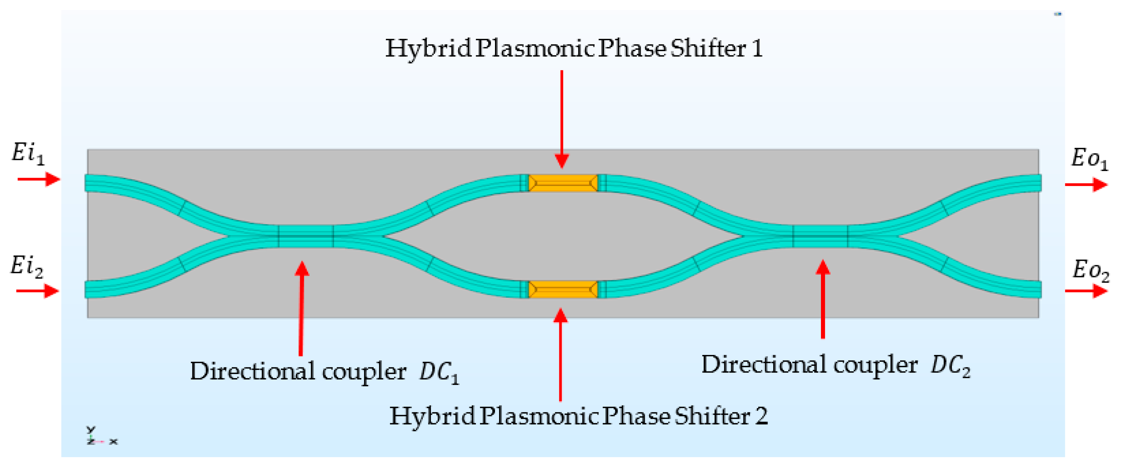
Figure 1. Basic configuration of 2 × 2 hybrid plasmonic MZS.
Photonics 06 00047 g001
Figure 2. (a) Cross section of the hybrid plasmonic waveguide phase shifter (HPWPS); (b) cross section of photonic waveguide; (c) 3D view of the designed hybrid plasmonic 2 × 2 MZS.
Photonics 06 00047 g002
Figure 3. 4 × 4 nonblocking plasmonic MZS with six control signals C a   to   C f .
Photonics 06 00047 g003
Figure 4. 2D (a) and 3D (b) schematics of the 4 × 4 plasmonic switch in the COMSOL environment.
Photonics 06 00047 g004
Figure 5. Scattering parameters of the 4 × 4 switch corresponding to the required transition state, T 1 k : from input 1 to the output port k (k = 5–8).
Photonics 06 00047 g005
Figure 6. Field intensity distributions at the four output ports when the signal is applied at input port 1, P 1 , and the required output port is P 6 .
Photonics 06 00047 g006
Figure 7. Crosstalk as a function of the transition number.
Photonics 06 00047 g007
Figure 8. Concept of using the optical switch as a router in optical networks. Six control signals are used to switch one of the four transmitters to one of the four receivers.
Photonics 06 00047 g008
Figure 9. Optical spectra at different points of the WDM optical network. (a) T x 1 output. (b) Switch fourth output port. (c) After 650 km transmission. (d) As in part c but the effect of fiber nonlinear optics is turned off in the used software.
Photonics 06 00047 g009
Figure 10. Eye diagrams of channel 1 (a), channel 4 (b), and channel 8 (c) of the fourth WDM receiver R x 4 after 13-span transmission.
Photonics 06 00047 g010
Figure 11. Optical spectra at the input and output ports of the designed 4 × 4 optical switch.
Photonics 06 00047 g011
Table 1. Dimensional parameters and material layers refractive indices (λ = 1550 nm) used in the design.
MaterialRefractive IndexWidth (nm)Height (nm)
Si 3.48200 (Photonic waveguide)200
100 (Plasmonic waveguide)
SiO 2 1.46200100
Polymer   ( JRD 1 ) 1.81
( r 33 = 390 pm/V)
1414
Ag 0.1444 + j11.3663030
Table 2. Operation states of the designed 4 × 4 optical switch. The control logic for each MZS is set to either logic 0 or logic 1 to denote cross state (∆Ø = 0) or bar state (∆Ø = π), respectively. The outputs are highlighted in red and green color to identify the cross state and bar state, respectively.
State No.Control LogicsOutput Power
C a C b C c C d C e C f P o 1 P o 2 P o 3 P o 4
1000000 P i 3 P i 4 P i 1 P i 2
2001000 P i 3 P i 2 P i 1 P i 4
3101000 P i 3 P i 1 P i 2 P i 4
4000100 P i 1 P i 4 P i 3 P i 2
5001100 P i 1 P i 2 P i 3 P i 4
6000010 P i 4 P i 3 P i 1 P i 2
7001010 P i 2 P i 3 P i 1 P i 4
8000110 P i 4 P i 1 P i 3 P i 2
9100110 P i 4 P i 2 P i 3 P i 1
10001110 P i 2 P i 1 P i 3 P i 4
11000001 P i 3 P i 4 P i 2 P i 1
12001001 P i 3 P i 2 P i 4 P i 1
13101001 P i 3 P i 1 P i 4 P i 2
14000101 P i 1 P i 4 P i 2 P i 3
15100101 P i 2 P i 4 P i 1 P i 3
16010101 P i 1 P i 3 P i 2 P i 4
17001101 P i 1 P i 2 P i 4 P i 3
18000011 P i 4 P i 3 P i 2 P i 1
19001011 P i 2 P i 3 P i 4 P i 1
20101011 P i 1 P i 3 P i 4 P i 2
21011011 P i 2 P i 4 P i 3 P i 1
22000111 P i 4 P i 1 P i 2 P i 3
23100111 P i 4 P i 2 P i 1 P i 3
24001111 P i 2 P i 1 P i 4 P i 3
Table 3. Crosstalk of the 4 × 4 plasmonic-based optical switch estimated at 1550 nm wavelength operation. 0 dBm input signal is used in the simulation.
Transition No.InputRequired Output PortOutput Power (dBm)Crosstalk (dB)
P 01 P 02 P 03 P 04
1 P 1 P 5 −7.65−32.15−33.00−34.00−24.50
2 P 6 −35.00−7.45−33.35−33.60−25.90
3 P 7 −39.00−46.50−7.40−36.30−28.90
4 P 8 −42.00−33.60−37.00−7.20−26.40
5 P 2 P 5 −7.35−31.90−39.00−32.10−24.55
6 P 6 −34.20−7.20−42.00−31.80−24.60
7 P 7 −41.50−34.20−7.20−31.40−24.20
8 P 8 −41.20−34.45−43.70−7.40−27.05
9 P 3 P 5 −7.40−40.00−35.90−51.20−28.50
10 P 6 −38.10−7.20−34.25−52.70−27.05
11 P 7 −35.65−45.10−7.65−40.15−28.00
12 P 8 −36.55−51.50−37.70−7.40−29.15
13 P 4 P 5 −7.20−32.60−32.50−31.90−24.70
14 P 6 −37.10−7.40−44.50−31.55−24.15
15 P 7 −35.65−41.55−7.40−41.18−28.25
16 P 8 −36.50−41.40−35.65−7.65−28.00
Table 4. Cross- and bar-states losses for each of the six MZSs used in the design of the 4 × 4 plasmonic switch.
2 × 2 SwitchCross Loss (dB)Bar Loss (dB)
A2.302.50
B2.302.50
C2.312.55
D2.312.55
E2.322.60
F2.322.60
Table 5. Performance comparison between the proposed switch and those in the literatures. All the switches have a 4 × 4 nonblocking configuration designed in silicon platform. The conventional switch in this table denotes a non plasmonic-based structure.
Switch TypePower Consumption V π L (V.µm)Footprint ( µ m 2 )Insertion Loss (dB)Crosstalk (dB)Phase Shifter Length (µm)
This work (plasmonic + EO)3.0 mW/π for 100 Gbps operation12550 × 707.70−26.56
Conventional (EO + thermo-optic) [8]33.7 mW/π3500 × 14007.70−12.0356
Conventional (EO) [47]25.0 mW/π256.255000 × 30003.00−25.0250
Conventional (EO) [48]20.0 mW/π2121600 × 3005.80−9.0200