Pancharatnam–Berry Optical Elements for Spin and Orbital Angular Momentum Division Demultiplexing

 ,
,  , ,
, , 
Abstract
:
1. Introduction
2. Materials and Methods
2.1. Phase Pattern Calculation
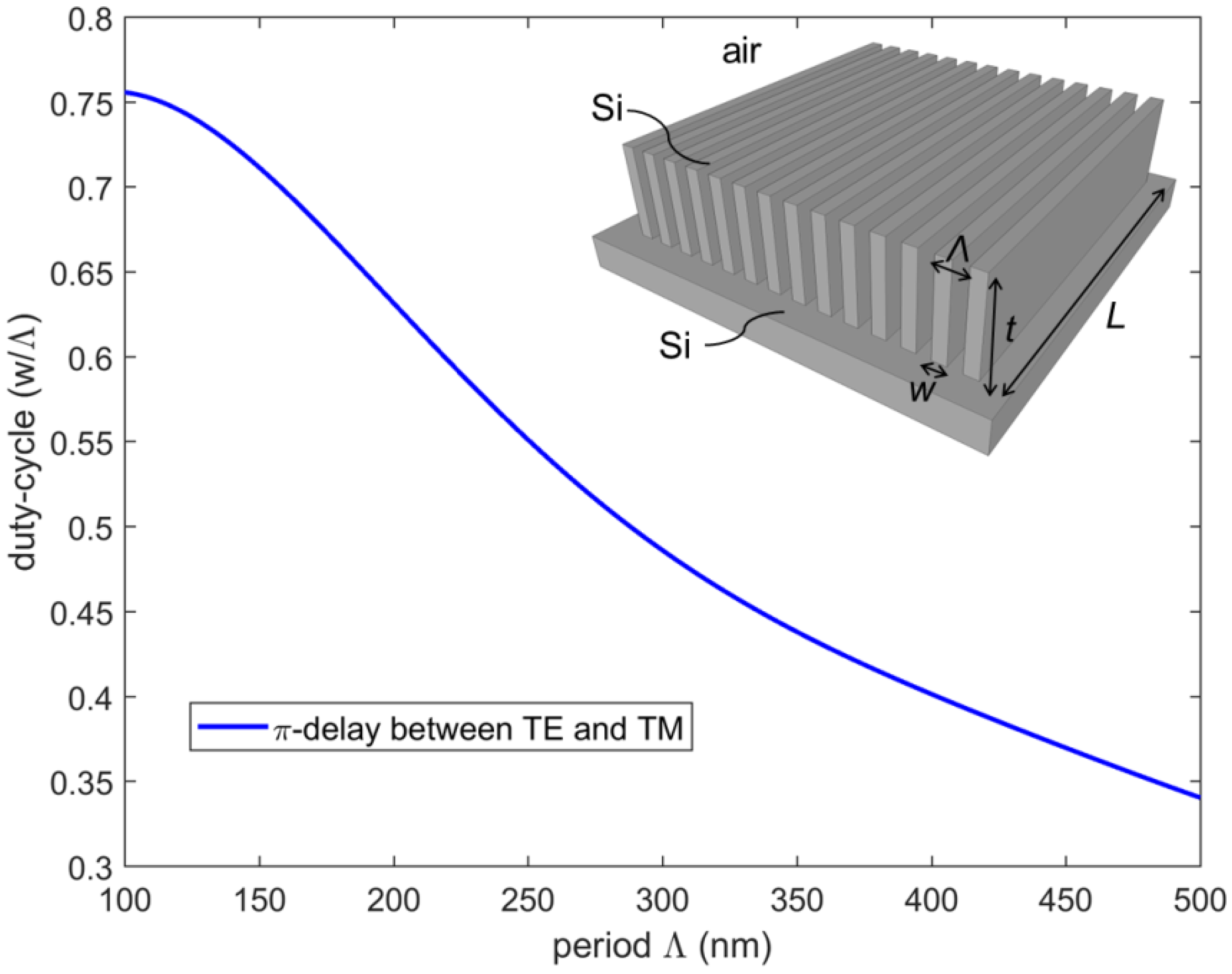
2.2. Subwavelength Grating Design
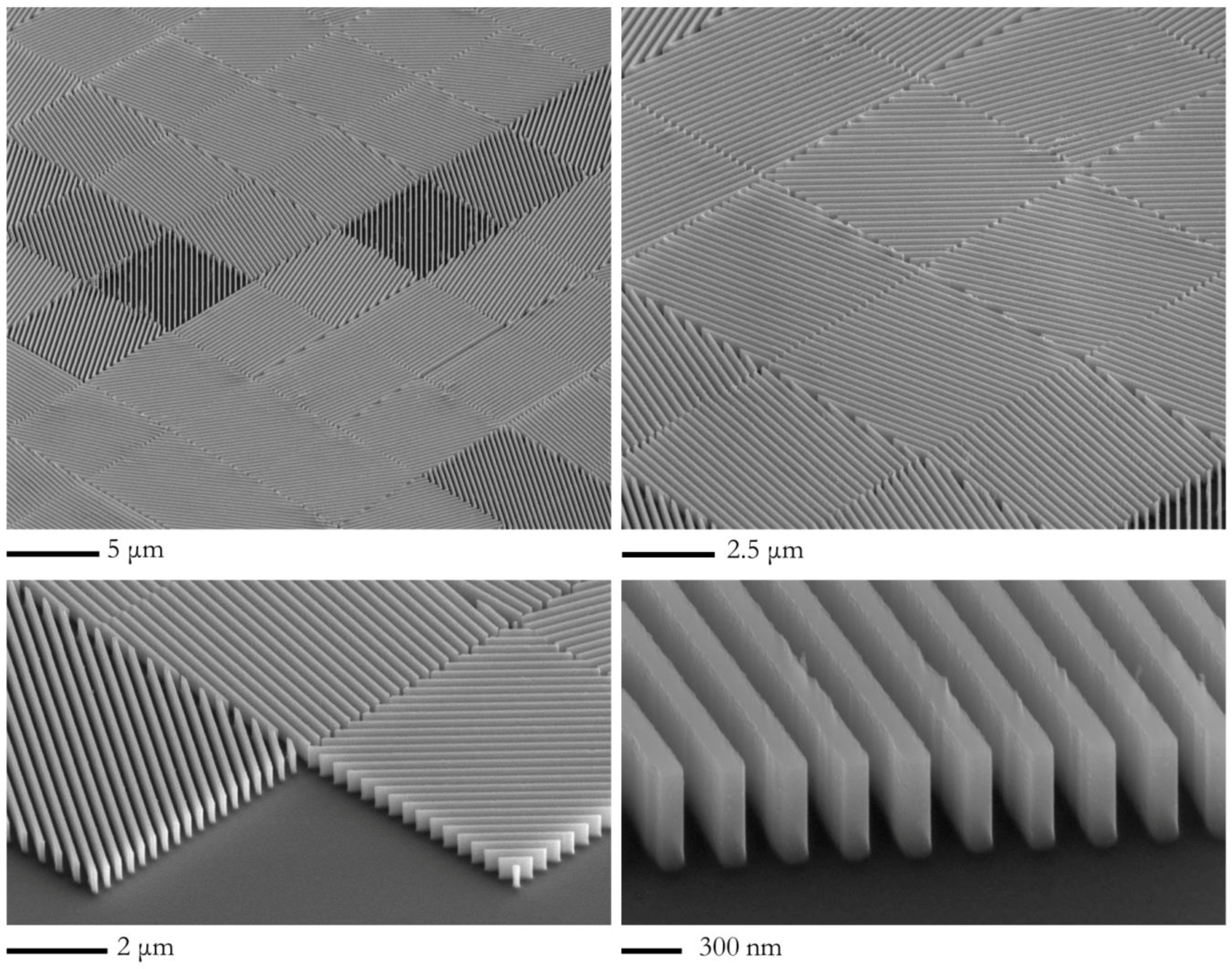
2.3. Fabrication
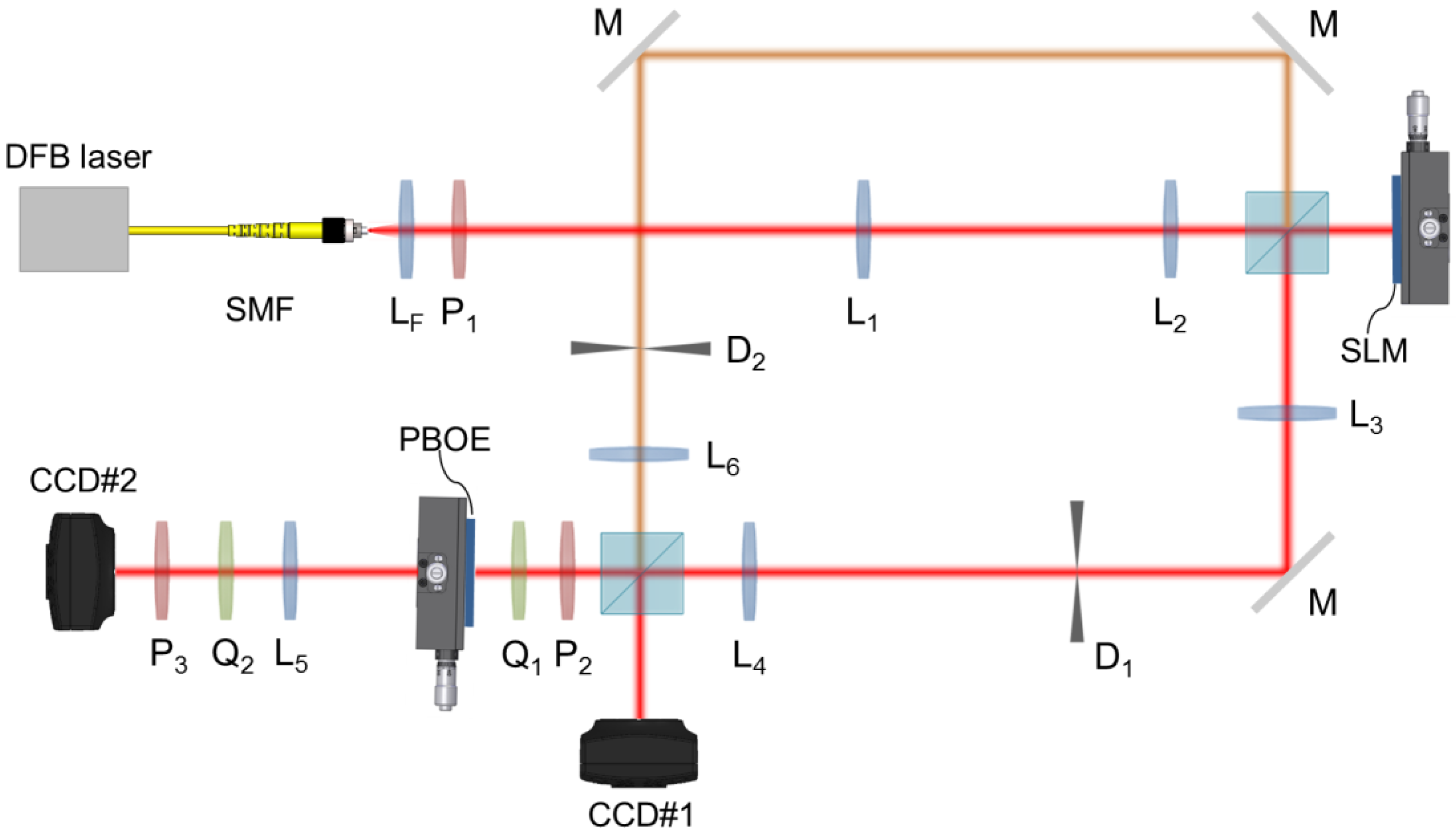
2.4. Optical Characterization Setup
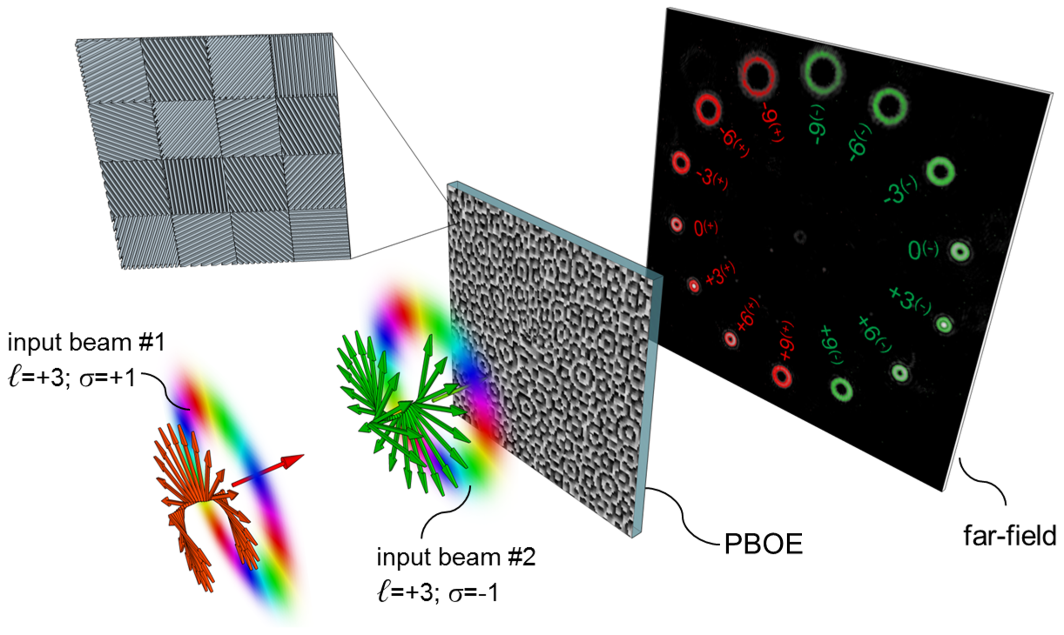
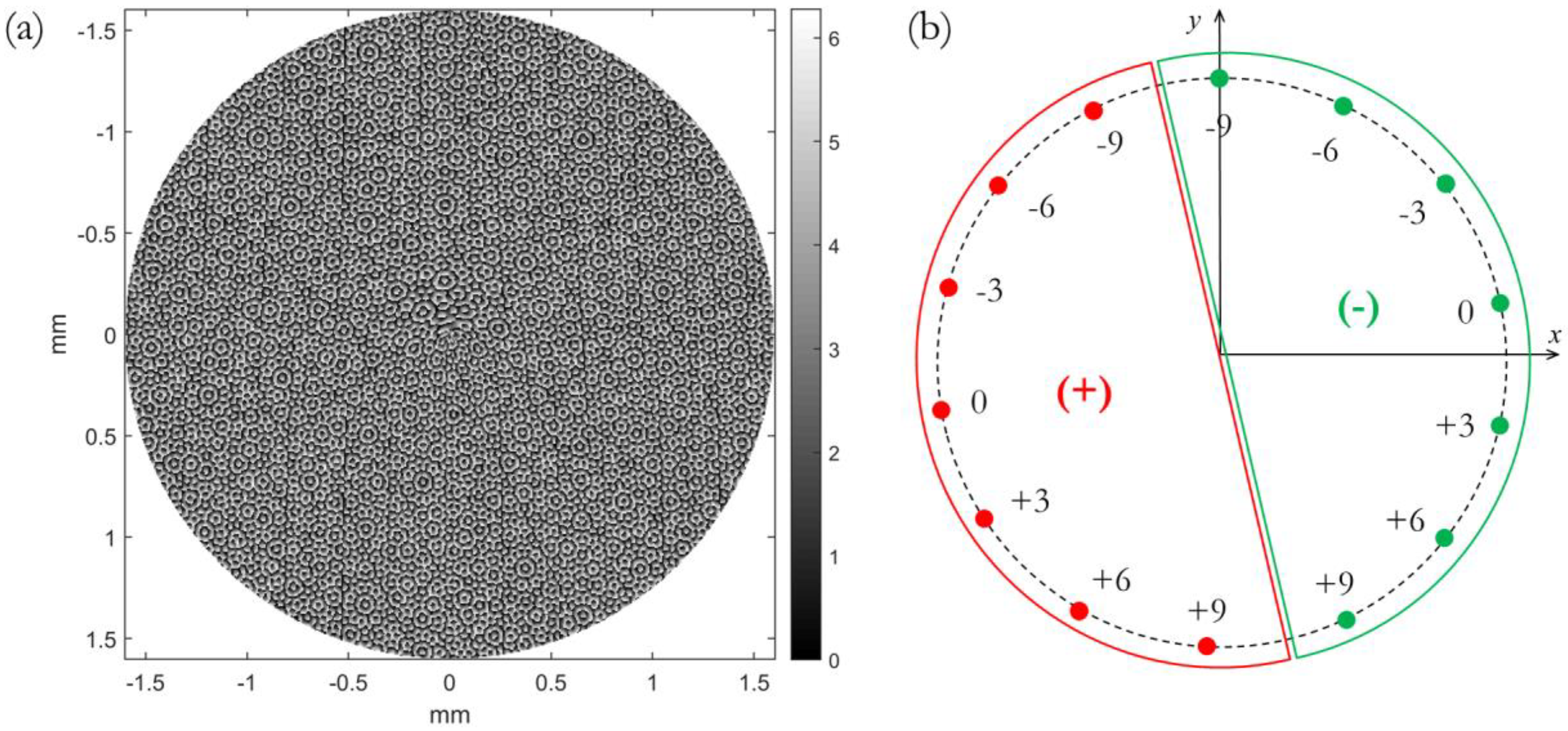
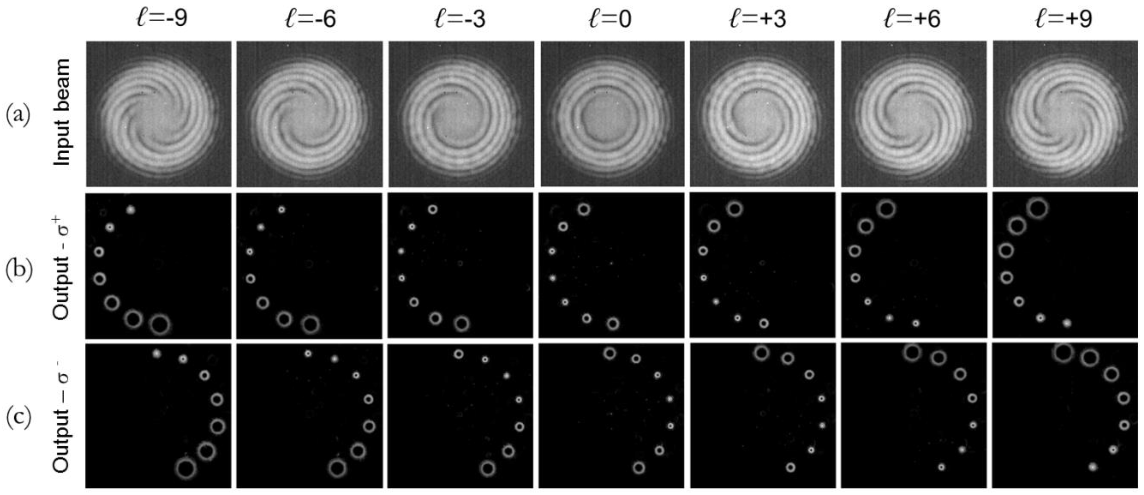
3. Results
4. Discussion
Author Contributions
Funding
Acknowledgments
Conflicts of Interest
Appendix A
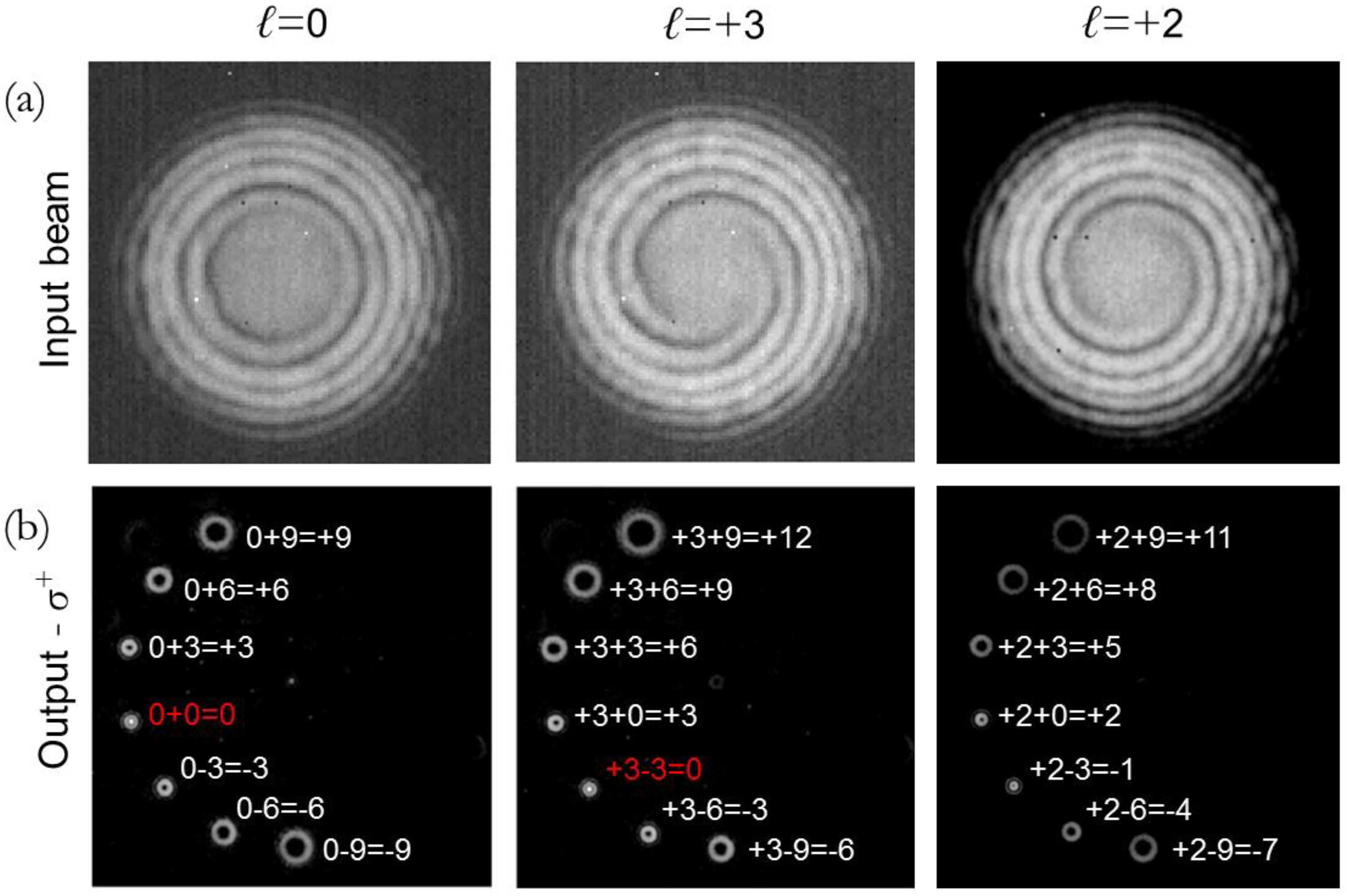
- input: ℓ = 0 -> output: {0 + 9, 0 + 6, 0 + 3, 0 + 0, 0 − 3, 0 − 6, 0 − 9} = {+9, +6, +3, 0, −3, −6, −9}
- input: ℓ = +3 -> output: {+3 + 9, +3 + 6, +3 + 3, +3 + 0, +3 − 3, +3 − 6, +3 − 9} = {+12, +9, +6, +3, 0, −3, −6}
- input: ℓ = +2 -> output: {+2 + 9, +2 + 6, +2+3, +2 + 0, +2 − 3, +2 − 6, +2 − 9} = {+11, +8, +5, +2, −1, −4, −7}.
Appendix B
References
- Agrell, E.; Karlsson, M.; Chraplyvy, A.R.; Richardson, D.J.; Krummrich, P.M.; Winzer, P.; Roberts, K.; Fisher, J.K.; Savory, S.J.; Eggleton, B.J.; et al. Roadmap of optical communications. J. Opt. 2016, 18. [Google Scholar] [CrossRef]
- Ramachandran, S.; Kristensen, P. Optical vortices in fiber. Nanophotonics 2013, 2, 455–474. [Google Scholar] [CrossRef]
- Andrews, D.; Babiker, M. The Angular Momentum of Light; Cambridge University Press: Cambridge, UK, 2013; ISBN 9781107006348. [Google Scholar]
- Mirhosseini, M.; Magana-Loaiza, O.S.; O’Sullivan, M.N.; Rudenburg, B.; Malik, M.; Lavery, M.P.J.; Padgett, M.J.; Gauthier, D.J.; Boyd, R.W. High-dimensional quantum cryptography with twisted light. New J. Phys. 2015, 17. [Google Scholar] [CrossRef]
- Bozinovic, N.; Yue, Y.; Ren, Y.; Tur, N.; Kristensen, P.; Huang, H.; Willner, A.E.; Ramachandran, S. Terabit-scale orbital angular momentum mode division multiplexing in fibers. Science 2013, 340, 1545–1548. [Google Scholar] [CrossRef] [PubMed]
- Yu, S. Potential and challenges of using orbital angular momentum communications in optical interconnects. Opt. Express 2015, 23, 3075–3087. [Google Scholar] [CrossRef] [PubMed]
- Willner, A.E.; Ren, Y.; Xie, G.; Yan, Y.; Li, L.; Zhao, Z.; Wang, J.; Tur, M.; Molish, A.F.; Ashrafi, S. Recent advances in high-capacity free-space optical and radio-frequency communications using orbital angular momentum multiplexing. Philos. Trans. A Math. Phys. Eng. Sci. 2017, 375. [Google Scholar] [CrossRef] [PubMed]
- Wan, C.; Rui, G.; Chen, J.; Zhan, Q. Detection of photonic orbital angular momentum with micro- and nano-optical structures. Front. Optoelectron. 2017, 1–9. [Google Scholar] [CrossRef]
- Ruffato, G.; Massari, M.; Romanato, F. Diffractive optics for combined spatial- and mode-division demultiplexing of optical vortices: Design, fabrication and optical characterization. Sci. Rep. 2016, 6, 24760. [Google Scholar] [CrossRef] [PubMed]
- Ruffato, G.; Massari, M.; Romanato, F. Compact sorting of optical vortices by means of diffractive transformation optics. Opt. Lett. 2017, 42, 551–554. [Google Scholar] [CrossRef] [PubMed]
- Ruffato, G.; Massari, M.; Parisi, G.; Romanato, F. Test of mode-division multiplexing and demultiplexing in free-space with diffractive transformation optics. Opt. Express 2017, 25, 7859–7868. [Google Scholar] [CrossRef] [PubMed]
- Ruffato, G.; Girardi, M.; Massari, M.; Mafakheri, E.; Sephton, B.; Capaldo, P.; Forbes, A.; Romanato, F. A compact diffractive sorter for high-resolution demultiplexing of orbital angular momentum beams. Sci. Rep. 2018, 8. [Google Scholar] [CrossRef] [PubMed]
- Gibson, G.; Courtial, J.; Padgett, M.J.; Vasnetsov, M.; Pas’ko, V.; Barnett, S.M.; Franke-Arnold, S. Free-space information transfer using light beams carrying orbital angular momentum. Opt. Express 2004, 12, 5448–5456. [Google Scholar] [CrossRef] [PubMed]
- Berkhout, G.C.G.; Lavery, M.P.J.; Courtial, J.; Beijersbergen, M.W.; Padgett, M.J. Efficient sorting of orbital angular momentum states of light. Phys. Rev. Lett. 2010, 105. [Google Scholar] [CrossRef] [PubMed]
- Roux, F.S. Geometric phase lens. J. Opt. Soc. Am. A 2006, 23, 476–482. [Google Scholar] [CrossRef]
- Chen, M.L.N.; Jiang, L.J.; Sha, W.E.I. Orbital Angular Momentum Generation and Detection by Geometric-Phase Based Metasurfaces. Appl. Sci. 2018, 8. [Google Scholar] [CrossRef]
- Desiatov, B.; Mazurski, N.; Fainman, Y.; Levy, U. Polarization selective beam shaping using nanoscale dielectric metasurfaces. Opt. Express 2015, 23, 22611–22618. [Google Scholar] [CrossRef] [PubMed]
- Li, Y.; Li, X.; Chen, L.; Pu, U.; Jin, J.; Hong, M.; Luo, X. Orbital Angular Momentum Multiplexing and Demultiplexing by a Single Metasurface. Adv. Opt. Mater. 2017, 5. [Google Scholar] [CrossRef]
- Emoto, A.; Nishi, M.; Okada, M.; Manabe, S.; Matsui, S.; Kawatsuki, N.; Ono, H. Form birefringence in intrinsic birefringent media possessing a subwavelength structure. App. Opt. 2010, 49, 4355–4361. [Google Scholar] [CrossRef] [PubMed]
- Kotlyar, V.V.; Khonina, S.N.; Soifer, V.A. Light field decomposition in angular harmonics by means of diffractive optics. J. Mod. Opt. 1998, 45, 1495–1506. [Google Scholar] [CrossRef]
- Moharam, M.G.; Pommet, D.A.; Grann, E.B.; Gaylord, T.K. Stable implementation of the rigorous coupled-wave analysis for surface-relief gratings: Enhanced transmittance matrix approach. J. Opt. Soc. Am. A 1995, 12, 1077–1086. [Google Scholar] [CrossRef]
- Kikuta, H.; Ohira, Y.; Kubo, H.; Iwata, K. Effective medium theory of two-dimensional subwavelength gratings in the non-quasi-static limit. J. Opt. Soc. Am. A 1998, 15, 1577–1585. [Google Scholar] [CrossRef]
- Ruffato, G.; Rossi, R.; Massari, M.; Mafakheri, E.; Capaldo, P.; Romanato, F. Design, fabrication and characterization of Computer-Generated Holograms for anti-counterfeiting applications using OAM beams as light decoders. Sci. Rep. 2017, 7. [Google Scholar] [CrossRef] [PubMed]
- Beck, M.; Graczyk, M.; Maximov, I.; Sarwe, E.L.; Ling, T.G.I.; Keil, M.; Montelius, L. Improving stamps for 10 nm level wafer scale nanoimprint lithography. Microelectron. Eng. 2002, 61–62, 441–448. [Google Scholar] [CrossRef]
- Pozzato, A.; Grenci, G.; Birarda, G.; Tormen, M. Evaluation of a novolak based positive tone photoresist as NanoImprint Lithography resist. Microelectron. Eng. 2011, 88, 2096–2099. [Google Scholar] [CrossRef]
- DePalma, V.; Tillman, N. Friction and Wear of Self-Assembled Trichlorosilane Monolayer Films on Silicon. Langmuir 1989, 5, 868–872. [Google Scholar] [CrossRef]
- Haensch, C.; Hoeppener, S.; Schubert, U.S. Chemical modification of self-assembled silane based monolayers by surface reactions. Chem. Soc. Rev. 2010, 39, 2323–2334. [Google Scholar] [CrossRef] [PubMed]
- Rosales-Guzmán, C.; Forbes, A. How to Shape Light with Spatial Light Modulators; SPIE Press: Bellingham, DC, USA, 2017; ISBN 9781510613027. [Google Scholar]
- Padgett, M.; Courtial, J.; Allen, L. Light’s Orbital Angular Momentum. Phys. Today 2004, 57, 35–40. [Google Scholar] [CrossRef]
- Jahani, S.; Jacob, Z. All-dielectric metamaterials. Nat. Nanotechnol. 2016, 11, 23–36. [Google Scholar] [CrossRef] [PubMed]
- Staude, I.; Schilling, J. Metamaterial-inspired silicon nanophotonics. Nat. Photonics 2017, 11, 274–284. [Google Scholar] [CrossRef]
- Vaity, P.; Rusch, L. Perfect vortex beam: Fourier transformation of a Bessel beam. Opt. Lett. 2015, 40, 597–600. [Google Scholar] [CrossRef] [PubMed]
- Goodman, J.W. Introduction to Fourier Optics; McGraw-Hill: New York, NY, USA, 1996; ISBN 9780070242548. [Google Scholar]
- Gradshteyn, I.S.; Ryzhik, I.M. Table of Integrals, Series, and Products Eighth Edition; Elsevier Academic Press: Waltham, MA, USA, 2015; ISBN 9780123849335. [Google Scholar]


© 2018 by the authors. Licensee MDPI, Basel, Switzerland. This article is an open access article distributed under the terms and conditions of the Creative Commons Attribution (CC BY) license (http://creativecommons.org/licenses/by/4.0/).
Share and Cite
Ruffato, G.; Capaldo, P.; Massari, M.; Mezzadrelli, A.; Romanato, F. Pancharatnam–Berry Optical Elements for Spin and Orbital Angular Momentum Division Demultiplexing. Photonics 2018, 5, 46. https://doi.org/10.3390/photonics5040046
Ruffato G, Capaldo P, Massari M, Mezzadrelli A, Romanato F. Pancharatnam–Berry Optical Elements for Spin and Orbital Angular Momentum Division Demultiplexing. Photonics. 2018; 5(4):46. https://doi.org/10.3390/photonics5040046
Chicago/Turabian StyleRuffato, Gianluca, Pietro Capaldo, Michele Massari, Alessia Mezzadrelli, and Filippo Romanato. 2018. "Pancharatnam–Berry Optical Elements for Spin and Orbital Angular Momentum Division Demultiplexing" Photonics 5, no. 4: 46. https://doi.org/10.3390/photonics5040046
APA StyleRuffato, G., Capaldo, P., Massari, M., Mezzadrelli, A., & Romanato, F. (2018). Pancharatnam–Berry Optical Elements for Spin and Orbital Angular Momentum Division Demultiplexing. Photonics, 5(4), 46. https://doi.org/10.3390/photonics5040046