1. Introduction
Micro-LEDs are light sources operating at very high current densities [
1], where the device self-heating, efficiency droop caused by Auger recombination, and surface recombination, become the major factors limiting the device performance. In particular, surface recombination results in a shift of the peak μ-LED efficiency towards higher current density, and in a decrease of the peak efficiency value when the device dimensions are reduced [
2,
3]. Earlier studies of μ-LEDs were focused primarily on their current-modulation characteristics [
4,
5,
6]. Only recently, the efficiency improvement had become a hot topic in the research and development of μ-LEDs. Typically, maximum values of external quantum efficiency (EQE) of μ-LEDs did not exceed 10% [
7,
8], which could be attributed to non-optimal light extraction from the LED dice. A record EQE of 42% at the current density of 50 A/cm
2 was recently demonstrated for 10 × 10 μm
2 devices and light extraction to silicone with the refractive index of 1.41 [
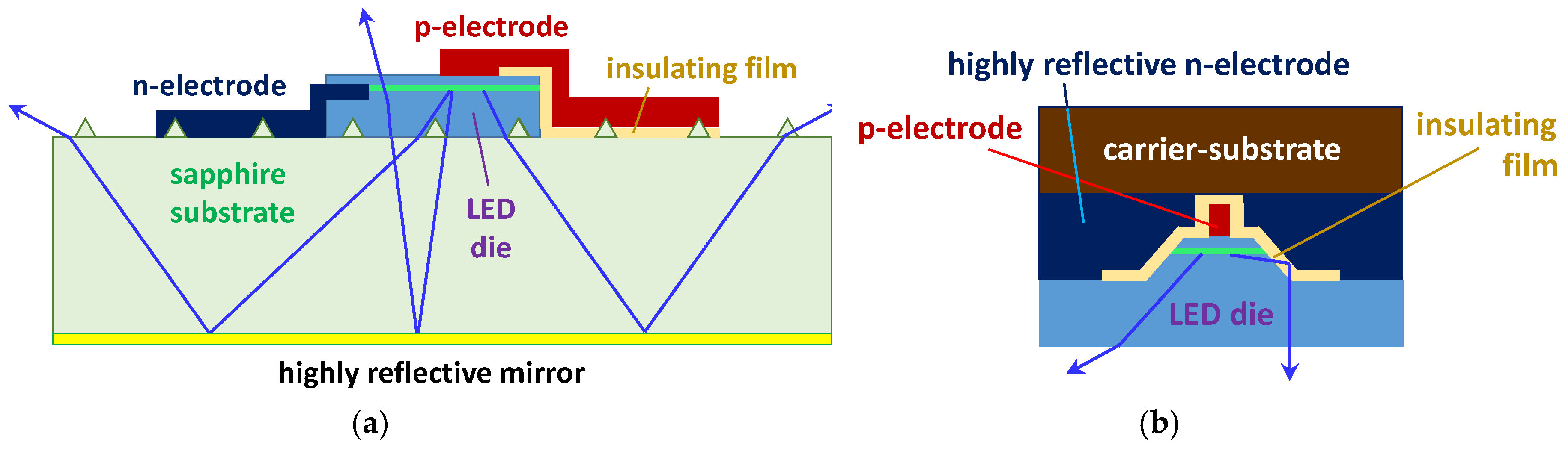
3]. Those μ-LEDs utilized profiled sapphire as the substrate for LED structures, and minimized the area of metallic electrodes on the emitting surface of the devices, in order to improve their LEE (see
Figure 1a for schematic design of the μ-LED die).
Being borrowed from the fabrication technology of large-size devices, the above approach seems, however, to be not quite suitable for μ-LEDs, frequently being components of high-density multipixel arrays. First, the feature dimensions of the profiled sapphire and periods of their sequence lies on the scale of a few microns. In this case, only a small number of the features fall into the μ-LED area. Therefore, LEE of such devices becomes dependent on both the number of the features and their particular arrangement inside the device area, which may vary randomly from sample to sample. In our opinion, just this factor was responsible, in particular, for the scatter and some irregular behavior of EQE as a function of μ-LED area, reported in [
3].
Second, the manner of light extraction from the μ-LEDs utilized in [
3] implies double-passing of emitted photons through the sapphire substrate, and their outgoing from the top emitting surface of the LED dice (see
Figure 1a). Here, the effective area of light emission becomes remarkably larger than a particular area of the μ-LEDs, which is clearly seen in the micrographs of the emission patterns reported in [
3]. This effect is undesirable for μ-LEDs operating in multipixel arrays.
Third, μ-LEDs normally operating at high current densities require an efficient heat removal from the active region. From this point of view, the chip design shown in
Figure 1a is not optimal, as the heat sinking occurs through a thick sapphire substrate having a rather low heat conductivity.
An alternative approach, suggested as a design unit of large-size AlGaInP red LEDs [
9], rather than for single μ-LEDs, was based on flip-chip device mounting on a heat sink. Here, inclined walls of the mesa, formed by etching after growing the LED structure, served as micro-reflectors for emitted photons (see
Figure 1b). After flip-chip mounting of the wafer on a carrier-substrate, the original substrate was removed, and the back surface of the n-contact layer was textured to increase LEE [
9]. The use of such micro-reflector seems to be quite promising for InGaN-based μ-LEDs, provided that geometry of the LED dice is carefully optimized with account of particular properties of nitride semiconductors and other materials employed.
To optimize a μ-LED design, modeling and simulation of its operation is a powerful approach. Since μ-LEDs operate frequently at extremely high current densities, electrical, thermal, and optical phenomena become strongly coupled with each other, generally requiring joint 3D simulations [
10]. A specific problem of such simulations is accurate accounting for temperature-dependent recombination coefficients related to non-radiative Shockley–Read–Hall (SRH), radiative, and Auger recombination, which is necessary for adequate prediction of thermal droop of the emission efficiency. As the recombination processes in InGaN quantum wells (QWs), serving as active regions in III-nitride LEDs, are interfered with by carrier localization due to composition fluctuations in InGaN alloys [
11,
12] and a strong electric field induced in polar InGaN QWs [
13], no consensus has currently been reached regarding temperature dependence of the recombination coefficients. Experimentally, there is a limited number of reports [
7,
14,
15] providing highly scattered and contradictory information on the dependence of recombination coefficients on temperature. Hence, this problem should be resolved in order to get predictive simulations of μ-LEDs.
In this paper, we will suggest a novel simulation approach using characterization data of conventional large-size LEDs as input information, making up for the lack of data on temperature-dependent recombination coefficients. Using this approach, an effective way for the efficiency improvement will be demonstrated based on shaping the μ-LED dice. Finally, the main characteristics of μ-LEDs with optimized design will be calculated and compared with those of large-size devices.
2. Simulation Approach and μ-LED Design
Simulation of μ-LED operation is carried out with the SimuLED package [
16] implementing a hybrid approach [
17], accounting self-consistently for current spreading, heat transfer, and light extraction in/from an LED die. Within the approach, the active region is simulated via (i) a relationship between the local density of current
j crossing the active region, and p–n junction bias
U, which is the electric potential drop between the lower and upper boundaries of the region, (ii) a dependence of the local internal quantum efficiency
ηi (IQE) on the current density
j, and (iii) a current density dependence of sheet carrier concentration
n2D injected into the active region assumed to be nearly the same for electrons and holes. In order to obtain the LED structure characteristics
j(
U),
ηi(
j), and
n2D(
j), direct simulations can be applied [
10], provided that temperature-dependent recombination coefficients are known with sufficient accuracy. Below, we will show how the above dependences can be extracted from characterization data of large-size LEDs, where the impact of surface recombination on LED characteristics is considered as negligible.
2.1. Approximation of LED Structure Characteristics
The dependence of p–n junction bias
U, on the current density
j, can be extracted from the current–voltage characteristic of an LED measured at a certain temperature
T. For this purpose, the characteristic should be fitted by the modified Shockley’s equation
where
Vf is the forward voltage,
j is the current density, i.e., the ratio of the LED operating current to the area of the active region,
ρS is the specific series resistance,
m is the ideality factor,
k is the Boltzmann constant,
q is the elementary charge, and
is the saturation current density with temperature-independent specific current density
j0 and activation energy
Ea.
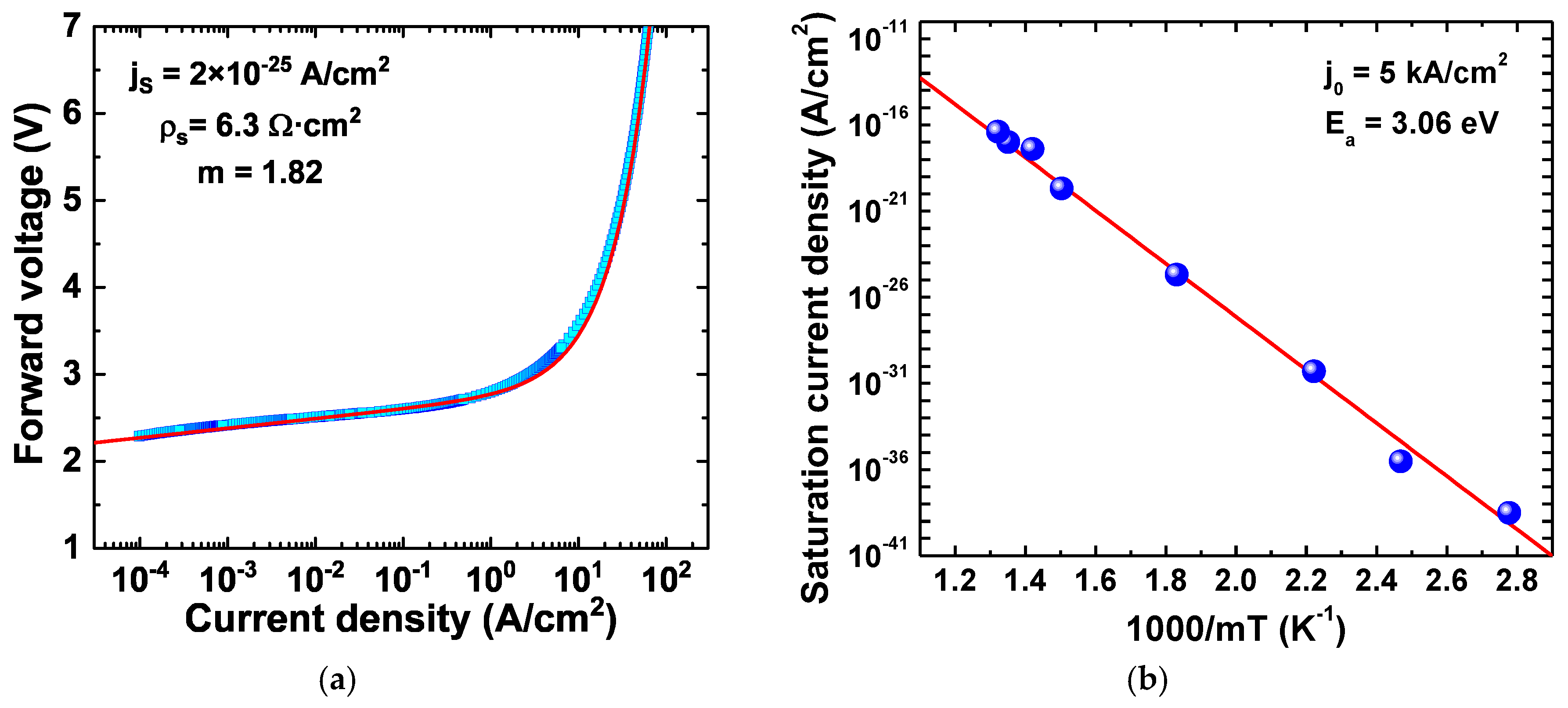
In order to estimate necessary parameters, we have used the data on temperature-dependent current–voltage characteristics of a blue (453 nm) 1 × 1 mm
2 MQW LED reported in [
18].
Figure 2a demonstrates excellent fitting of the experimental characteristic corresponding to 300 K by Equation (1) and shows the parameters
jS,
ρS, and
m extracted from the fitting. Processing of the data reported in [
18] for temperatures varied from 200 K to 440 K, provides the ideality factor
m = 1.8 ± 0.1, which is practically constant in the above temperature range. Also, the saturation current density
jS varies exponentially with the prefactor
j0 = 5 kA/cm
2 and activation energy
Ea = 3.06 eV. The activation energy is higher than the energy gap of InGaN QW in the LED active region, but it is lower than the bandgap of GaN barriers cladding the QWs.
The dependence of internal quantum efficiency
ηi on the current density
j is derived by using the ABC recombination model considering three main recombination channels: SRH non-radiative recombination with the coefficient
A, radiative recombination with the coefficient
B, and Auger recombination with the coefficient
C. The model neglects the electron leakage from the LED active region to p-layers of the LED structure, and assumes the concentrations of electrons and holes in the active region to be nearly equal to each other. Within the ABC-model, current density and IQE of an LED can be calculated by the expressions [
19,
20]:
Here, the normalized output power
is the ratio of the LED output power
Pout at a certain current to the power
Pm at the EQE peak,
jm is the current density corresponding to the EQE peak, and
Q is the dimensionless combination of the recombination constants
A,
B, and
C. Using conventional characterization data, i.e., dependence of EQE on the LED operating current, one can directly obtain
Pm and
jm, and extract
Q-factor by a special procedure suggested in [
18]. The data of [
18] provide the following approximations for the blue MQW LED:
, where
Q0 = 110 and
TQ = 134 K, and
, where
P0 = 0.17 mW and
TP = 67 K. Using them, it is possible to estimate the current density
jm by the following expression:
, where
S = 0.01 cm
2 is the active region area,
Eph = 2.74 eV is the mean energy of emitted photons, and
ηext is LEE, linearly decreasing from 71% to 68% as the temperature varied from 200 K to 440 K [
18]. Finally, the IQE dependence on
j corresponding to a particular temperature can be obtained from Equation 2 by varying the normalized power
p in an appropriate range. It has been shown in [
18] that Equation (2) fits, very accurately, the experimental EQE dependence on operating current/output power of the LED in a wide range of its variation.
The sheet concentration of carriers
n2D, injected in the LED active region, can also be obtained within the ABC-model. In terms of the variables discussed above,
In contrast to IQE, evaluation of sheet carrier concentration requires knowledge of the SRH recombination coefficient
A in addition to the parameters
jm and
Q. The temperature dependence of
A-coefficient has been reported recently for blue and green LEDs [
15]; both data can be well approximated by the expression
, where
A0 = 8000 s
−1 and
TA = 65 K. Combination of Equations (2) and (3) provides a parametric dependence of
n2D on the current density
j.
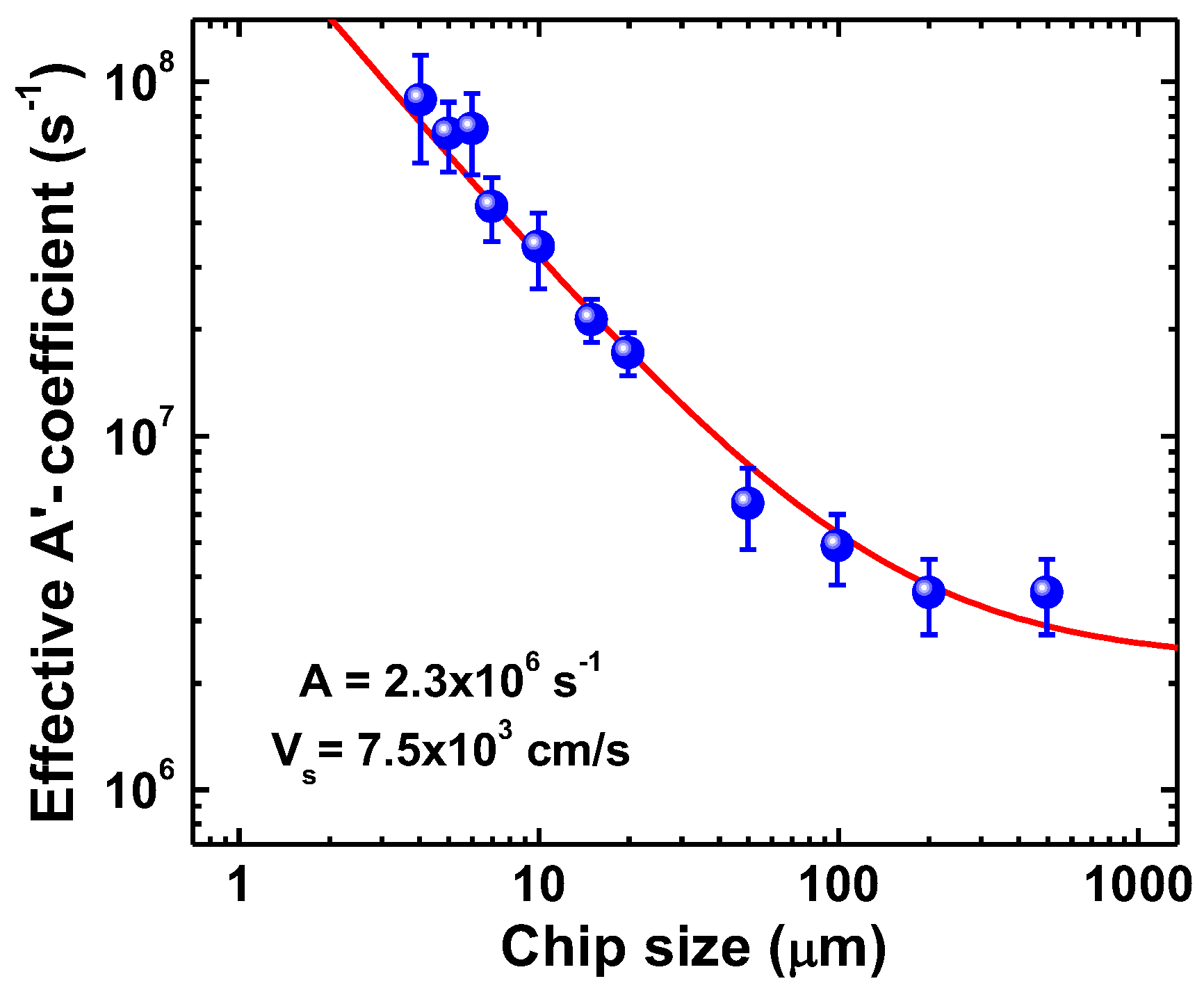
2.2. Evaluation of Surface Recombination Velocity
Surface recombination is accounted for in our simulations via boundary conditions for 2D carrier transport equations in the LED active region [
21]. As it was mentioned previously [
21], the surface recombination velocity
VS is known for InGaN materials with insufficient accuracy. In order to evaluate its value more accurately, we used the recent data [
22] on the size-dependent effective SRH recombination coefficient
A’, which is related to the perimeter
and area Σ of the LED active region, via an approximate equation valid for sufficiently small devices [
10,
23]:
Approximating the data of [
22] by the above expression (see
Figure 3), we have obtained
VS = 7.5 × 10
3 cm/s. This value is 7.5 times higher than that assumed in our previous simulations [
10]. Due to the lack of data on the temperature dependence of surface recombination velocity, we used the above value in the whole range of temperature variation.
2.3. Design of μ-LED Dice and Material Parameters
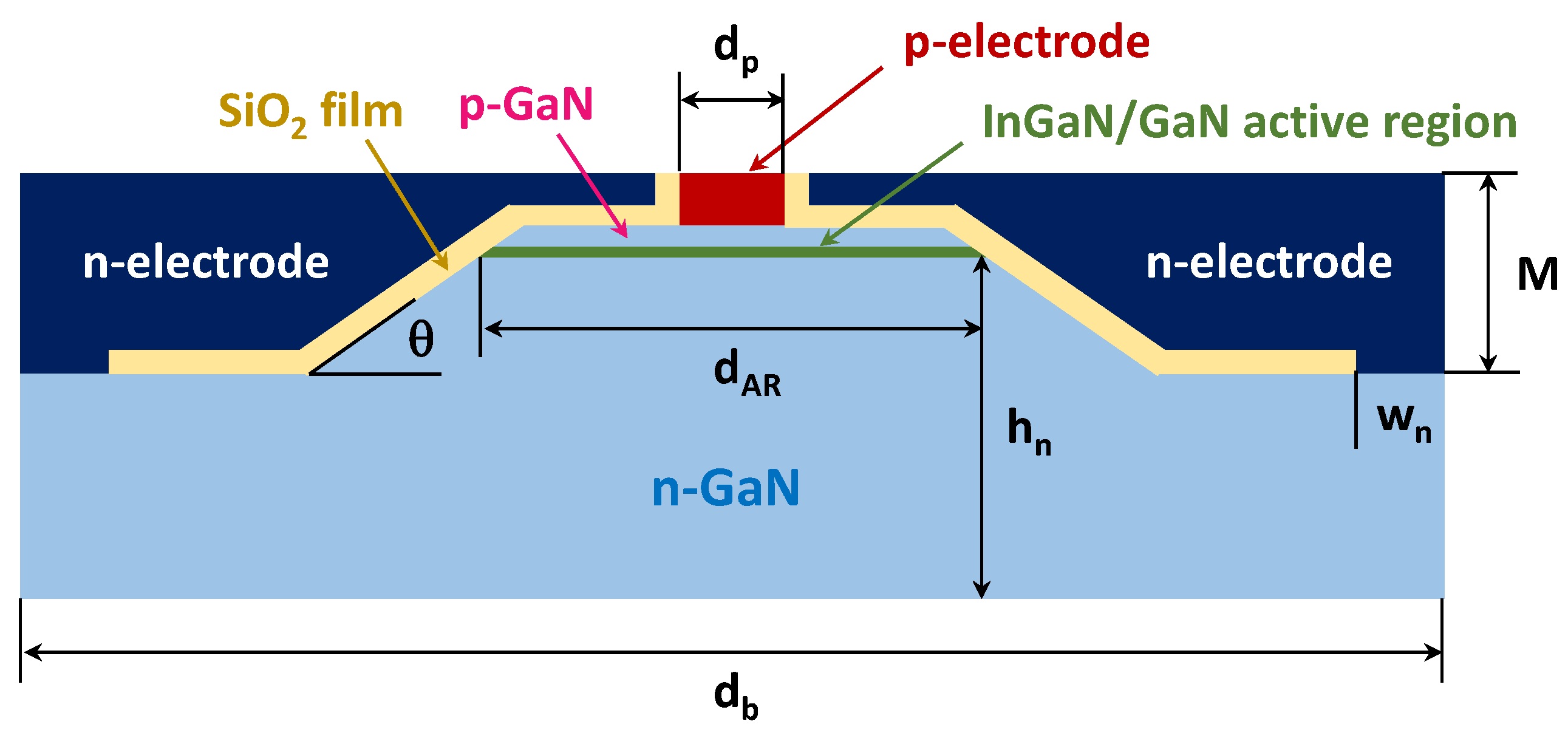
Design of a flip-chip blue μ-LED die with truncated-pyramid shape and various inclinations of the side mesa facets, considered in our study, is shown schematically in
Figure 4. Every die had a lateral dimension of the base
db, a lateral size of InGaN-based active region
dAR, a lateral size of the p-electrode
dp, a mesa depth
M, and a width of the n-contact
wn. Variation of the mesa facet inclination angle
θ, used in our simulations, did not change the dimensions of active region (
dAR) and μ-LED die (
db, dp, and
wn). The thicknesses of the n-GaN contact layer
hn = 5 μm, and p-GaN contact layer
hp = 0.2 μm, were also fixed in the simulations.
We considered two types of μ-LEDs: small μ-LEDs with dp = 1 μm, dAR = 5 μm, db = 15 μm, and wn = 3 μm, and large μ-LEDs with those dimensions enlarged by a factor of four, i.e., dp = 4 μm, dAR = 20 μm, db = 60 μm, and wn = 12 μm. Besides, in the case of small μ-LEDs, we considered two kinds of mesas: a shallow mesa with M = 1.0 μm and a deep mesa with M = 2.4 μm. The size of p-electrode was intentionally chosen much smaller than dAR, in order to prevent carriers injected into the LED active region from surface recombination at its edges.
The n-GaN contact layer was assumed to be doped with Si up to the donor concentration ND = 1×1019 cm−3 (ionization energy of donors is 13 meV), and to have a temperature-independent mobility of 100 cm2/V·s. The p-GaN contact layer was assumed to be doped with Mg up to the acceptor concentration NA = 3×1019 cm−3 (ionization energy of acceptors is 170 meV), and to have the hole mobility decreasing with temperature from 10 cm2/V·s at 300 K to 6 cm2/V·s at 600 K. Temperature dependence of both electron and hole concentrations in the contact layers was accounted for in our simulations. The specific resistances of n- and p-contacts were chosen to be 10−5 Ω·cm2 and 10−4 Ω·cm2, respectively.
Reflectivity of n- and p-electrodes were simulated using the optical constants of silver and gold, respectively [
24], being the basic materials for the contacts. The refractive indexes of 2.48 and 1.465 were chosen for GaN and SiO
2 insulating film, respectively, corresponding to the emission wavelength of 453 nm. The main substrate was assumed to be removed after growth of LED structure. No intentional surface texturing was assumed on free semiconductor surfaces, including back surface of the n-GaN contact layer, so that the surfaces provided Fresnel reflection of light dependent on its polarization.
The heat was assumed to release through the top surfaces of the μ-LED dice. The heat sinking was accounted for via heat transfer coefficient of 1×10⁵ W/K·m2. Temperature-independent heat conductivity of 120 W/K·m was chosen for all GaN-based contact layers.
3. Results
Simulations of μ-LEDs shown schematically in
Figure 4 were carried out in two stages. At the first stage, we optimized the shape of the μ-LEDs, including inclination angle of mesa facets and die dimensions. Using the optimized shape of the μ-LED dice, the output characteristics of the devices were calculated at the second stage, in order to compare them with those of large-size LEDs. The results of the simulations are summarized below.
3.1. Optimization of Insulating Layer Thickness
One can see in
Figure 4 that the μ-LED die contacts mostly with the highly reflective metal through the insulating film made of SiO
2. This film influences, remarkably, the reflectivity of light emitted from the active region.
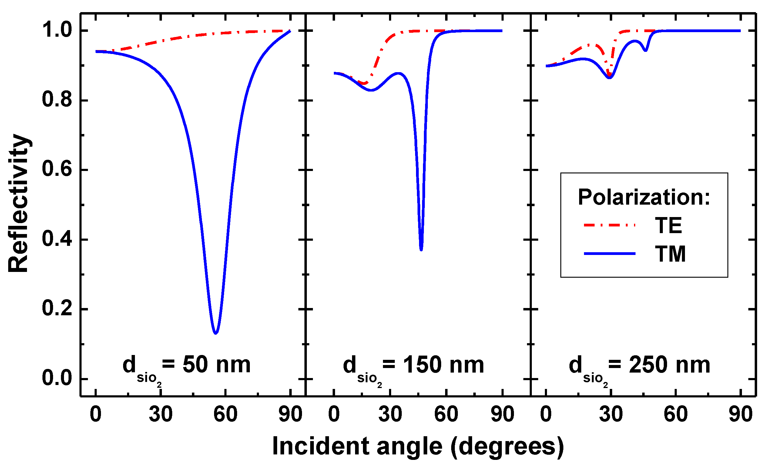
Figure 5 shows the reflection coefficients of photons with the wavelength of 453 nm versus their incident angle calculated for SiO
2 films of various thicknesses placed on bulk Ag, which is the basic material of n-electrode. The calculations were carried out for two polarizations of the incident light: transverse-electric (TE) and transverse-magnetic (TM), accounting for interference of photons reflected from the SiO
2/GaN and Ag/SiO
2 interfaces. At small SiO
2 thickness (
dSiO2 = 50 nm), the reflectivity of TE-polarized light is higher than 90% in the whole range of the incident angles. However, there is a remarkable dip in the reflectivity of TM-polarized light at the angles close to the Brewster angle of silver. As photons traveling inside the μ-LED die change their incidence angle and polarization from one reflection to another, the above dip results in higher optical losses caused by incomplete reflection and, eventually, in a lower LEE.
When the thickness of the SiO
2 film is increased up to the value, comparable with the light wavelength in SiO
2, i.e., about 305 nm (see
Figure 5), the dip magnitude is reduced considerably at the expense of slight reduction in the reflectivity of TE-polarized light. This occurs due to a constructive interference of TM-polarized photons reflected from SiO
2/GaN and Ag/SiO
2 interfaces. As a result, LEE of the μ-LED dice with thicker SiO
2 film tends to rise. Increasing the thickness of the film above 250 nm no longer leads to further LEE improvement. Therefore,
dSiO2 = 250 nm has been regarded as the optimal value permanently used in subsequent simulations.
3.2. Optimization of μ-LED Die Shape
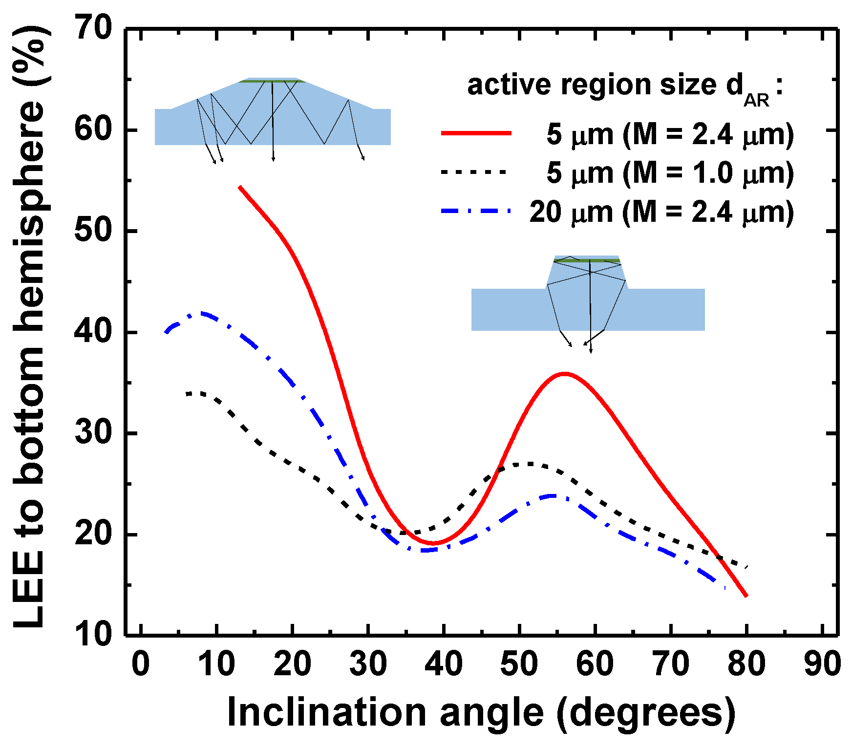
Shape optimization for the μ-LED dice was carried out by SimuLED package [
16] using LEE to the bottom hemisphere of the die (see
Figure 4) as the optimization target. LEE was determined by 3D ray tracing assuming light extraction to air and accounting for polarization of light. Uniform distribution of the emission intensity over the μ-LED active region is assumed in the simulations. Two million rays were found to be sufficient for predicting LEE with an accuracy of 0.1%. We have considered both small and large μ-LEDs (see
Section 2.3); in the former case, we have performed the simulations for a shallow (
M = 1.0 μm) and a deep (
M = 2.4 μm) mesa. Variation of the mesa-facet inclination angle was made in a wide range only limited by a particular geometry of the μ-LED dice.
Figure 6 demonstrates a non-monotonous dependence of LEE to the bottom hemisphere on the mesa-facet inclination angle, computed for the above μ-LED designs. In all three cases considered, there are two distinct maxima of LEE with a minimum between them. The strongest LEE maximum is observed at glancing angles of 8–13°. This effect can be interpreted in terms of light propagation in a laterally tapered waveguide formed by the bottom surface of the μ-LED die, and inclined facets of the mesa. The taper turns directions of photons propagating inside the μ-LED die at every reflection from the n-electrode providing, eventually, effective light extraction through the bottom surface of the die (see inset in
Figure 6). The magnitude of the second LEE maximum is lower than that of the first one by a factor of about 1.5. It exists, tentatively, due to micro-reflectors formed by the inclined mesa facets, largely focusing the emitted light in the direction normal to the bottom surface of the μ-LED die. A minimum of LEE, observed in
Figure 6 between 35° and 45°, corresponds to non-optimal facet inclinations producing high optical losses of light captured by the μ-LED die.
Breakdown of the optical losses (not shown here) has revealed two principal mechanisms of them. The strongest one is incomplete light reflection from the metallic n-electrode. The losses relevant to this mechanism consume from 25% (at optimal shape of the die) to 55% of emitted photons, with the strong maximum corresponding to non-optimal facet inclinations, i.e., at the inclination angles between 35° and 45°. The latter means that non-optimal inclination of the mesa facets provides a larger number of light reflections from the n-electrode than in the case of optimized μ-LED shape.
The second in the rank of importance mechanism of optical losses is free-carrier absorption in the thick heavy-doped n-GaN contact layer. The donor concentration of 1×1019 cm−3 provides, here, the room-temperature free-electron absorption coefficient of 10.7 cm−1. The losses by this mechanism consume from 10% (at optimal shape of the die) to 25% of emitted photons, depending on particular μ-LED design, with a rather weak dependence on the inclination angle.
Comparison of LEEs of large and small μ-LED with different mesa depths enables making the following conclusions. First, at the same mesa depth and thicknesses of n- and p-contact layers, the large μ-LED has a remarkably lower LEE. Second, a deeper mesa in the small μ-LED provides a higher LEE. These conclusions are important, pointing out the fact that maximum LEE can be achieved, if (i) the length of the inclined facets exceed, remarkably, the lateral size of the active region, and (ii) the mesa depth is comparable with the total thickness of the LED structure.
3.3. Current Density-Dependent Light Extraction Efficiency
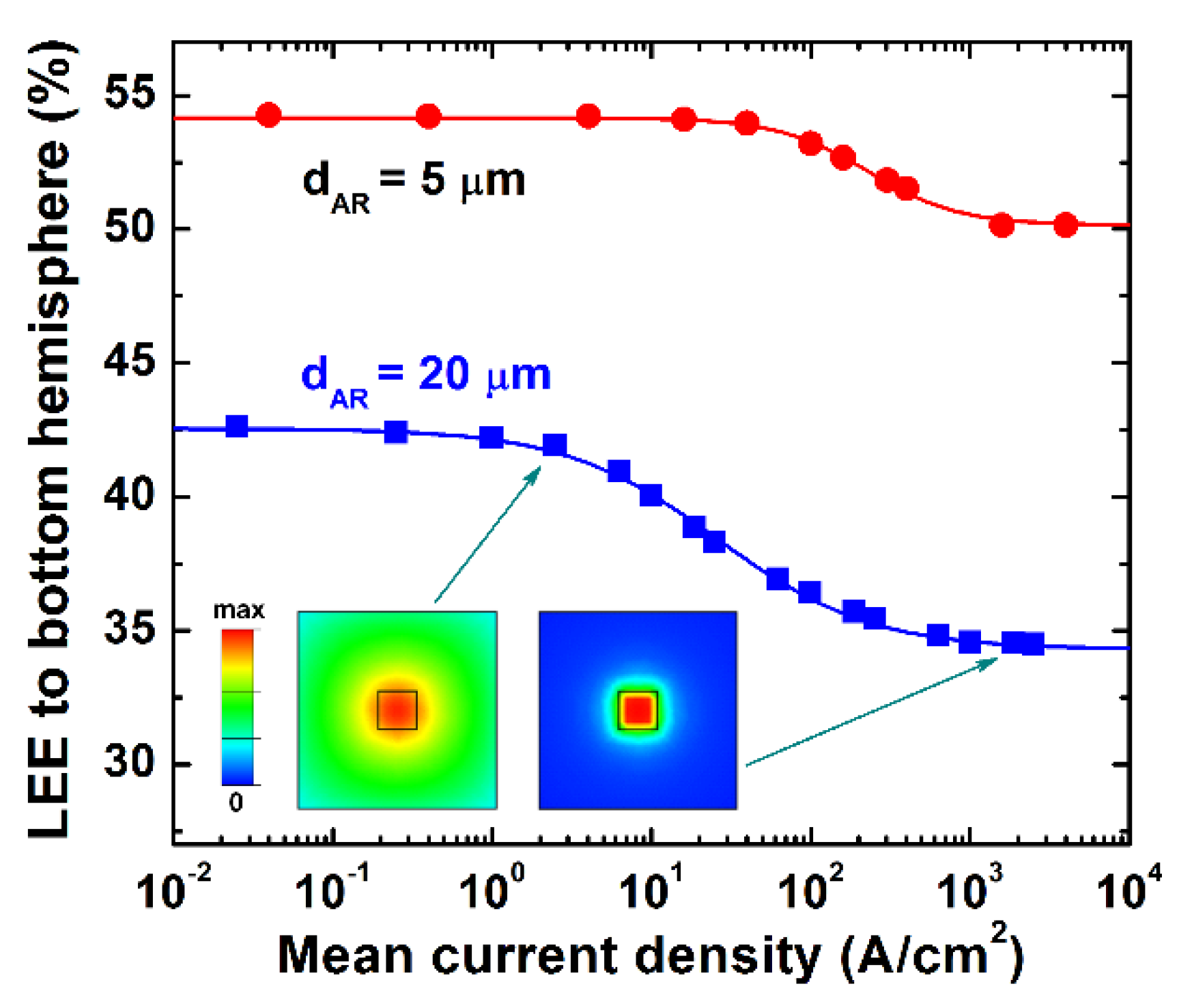
The above simulations, aimed at optimizing the shape of the μ-LED dice, were carried out by assuming the emission intensity to be uniformly distributed over the active region. This assumption is, however, invalid at high-current operation of μ-LEDs because of current crowding. In order to take this effect into account, we have carried out self-consistent electrical-thermal-optical simulations of μ-LEDs, with optimized shapes of the dice: dAR = 5 μm, M = 2.4 μm, and θ = 13° for small, and dAR = 20 μm, M = 2.4 μm, and θ = 8° for large devices.
Figure 7 shows LEEs to the bottom hemisphere of large and small μ-LEDs as a function of mean current density in the active region, which is the ratio of the operating current to the active region area. One can see that, in both types of μ-LED, LEE starts to decrease towards higher current densities. The reason for the LEE reduction is localization of the non-equilibrium carriers under the poorly reflective Au-based p-electrode. This is clearly seen in 2D-distributions of sheet carrier concentration in the active region displayed in insets of
Figure 7. At a low current density, the carriers are more or less uniformly distributed, producing LEE close to that predicted for uniform emission intensity in the active region. At a high current density, the carriers are largely localized under the p-electrode, exhibiting higher optical losses caused by incomplete light reflection from the metal. The higher the current density, the stronger the current crowding, and the lower LEE becomes, as is shown in
Figure 7. The predicted evolution of LEE (
ηext), with the mean current density, can be well approximated by the function
where
η0 is the low-current LEE, Δ
η is the magnitude of the LEE reduction at high currents,
jc is the current density at which current crowding reduces LEE by the half-value of Δ
η, and
γ is the specific exponent. We have found
η0 = 54.4%, Δ
η = 4.3%,
jc = 230 A/cm
2, and
γ = 1.5 for small μ-LEDs, and
η0 = 42.6%, Δ
η = 8.3%,
jc = 26 A/cm
2, and
γ = 0.9 for large μ-LEDs. Comparison of the parameters shows that current crowding starts to affect LEE at lower current densities, and produces a higher LEE reduction in large devices. This conclusion is in line with those made in our previous study on scaling μ-LED dimensions [
10].
3.4. Output Characteristics of μ-LEDs
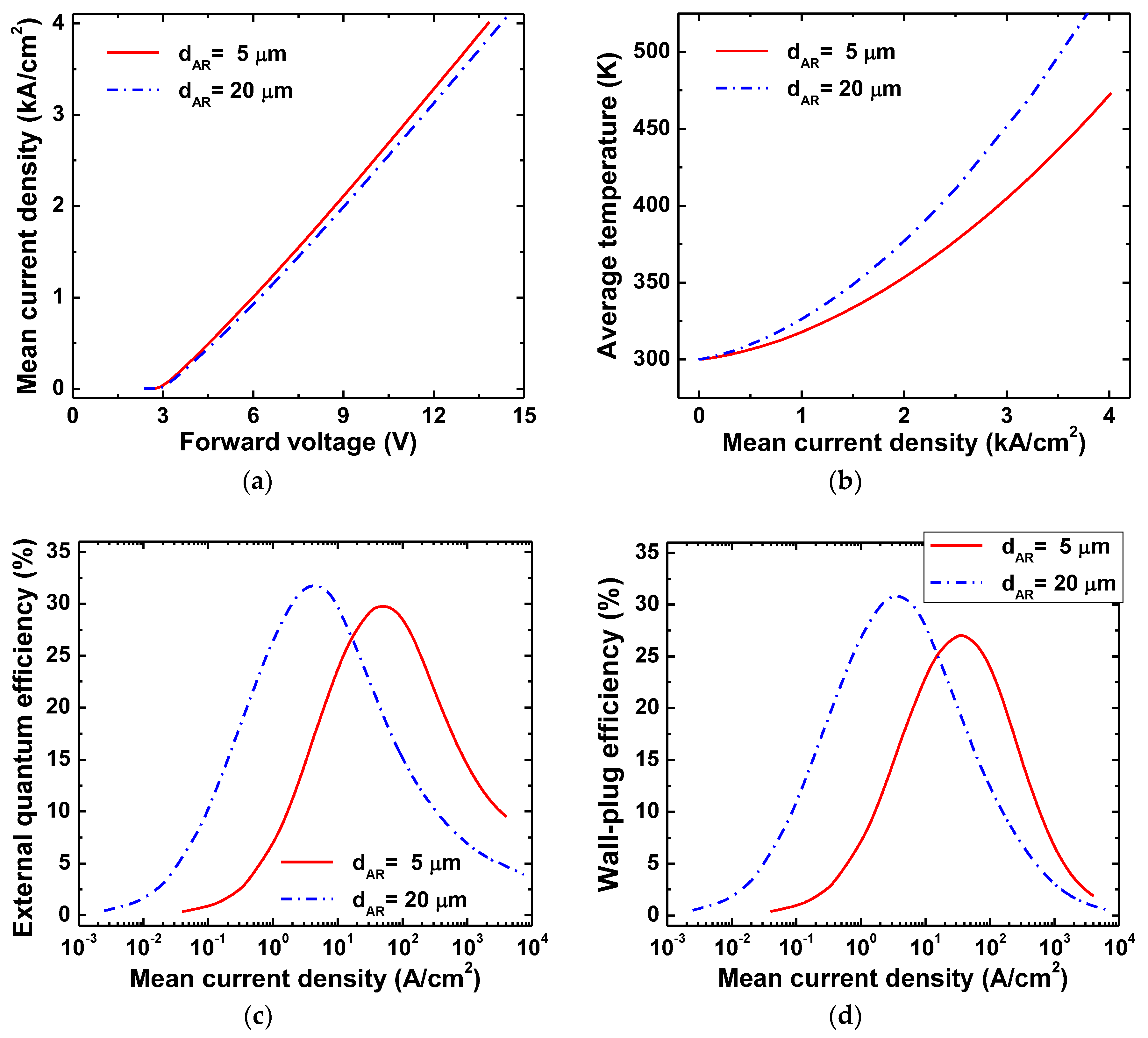
The output characteristics of μ-LEDs have been simulated for small and large devices, having optimized mesa facet inclinations, with account of current-dependent LEE.
Figure 8a demonstrates that current density–voltage characteristics of both μ-LEDs are close to each other with the slope, corresponding to specific series resistance of 2.71 ± 0.05 mΩ·cm
2. Analysis of the electric potential distributions in the μ-LED dice has shown that the major contribution to the specific series resistance of the devices comes from the p-contact. Indeed, because of the small area of p-electrode (see
Section 2.3 for description of μ-LED design), the current density at the p-electrode is 25 times higher than the mean current density in the μ-LED active region. Therefore, at the specific contact resistance of 10
−4 Ω·cm
2 assumed in our simulations, this provides the μ-LED-specific series resistance of 2.5 mΩ·cm
2, which is slightly less than the value estimated directly from the current density–voltage characteristics shown in
Figure 8a.
Figure 8b displays dependence of the average temperature in the active region on the mean current density. One can see that, at the same current density, large μ-LED exhibits a stronger self-heating compared to a small device. The reason for the effect is stronger current crowding in large μ-LED, as it was discussed in detail earlier [
10]. A considerable, i.e., more than by 50 K, overheating of the LED active region is predicted for current densities greater than 1.5–2.0 kA/cm
2. Below 1 kA/cm
2, the thermal effects, including the thermal efficiency droop, may be regarded as negligible.
Simulated EQEs of the μ-LEDs are plotted versus mean current density in
Figure 8c. Here, total LEE to air, and its dependence on the current density, has been taken into account, instead of LEE to the bottom hemisphere. First, the current density corresponding to the efficiency peak is shifted to higher values in small μ-LED. Being in agreement with a general trend of scaling the μ-LED dimensions, this effect originates from surface recombination at the active region edges, which is especially critical in small-size devices [
10]. The relative difference between the peak EQEs of large and small μ-LEDs, i.e., 31.7% and 29.7%, is smaller than the difference in their IQEs, i.e., 68% and 51%, respectively, which is due to a higher LEE of the small μ-LED, as it has been demonstrated in
Section 3.2. The relative difference between the peak wall-plug efficiencies (WPEs) of large and small μ-LEDs, i.e., 30.8% and 27.0%, respectively, is higher than the difference between EQEs. This is attributed to the fact that the peak EQE of the small μ-LED corresponds to a higher current density, producing a higher operating voltage, thus reducing WPE.
The carrier losses by surface recombination at the current densities at EQE peak are found to be of nearly 15% and 20% for large and small devices, respectively. Such relatively small losses are due to the small dimensions of the p-electrode, localizing the injected carriers far from the active region edges.
4. Discussion
The most important conclusion following from our simulations is that optimizing the shape of a μ-LED die enables considerable LEE improvement, as compared to large-size devices. Since no profiled sapphire substrate or intentional texturing of emitting surfaces was assumed in the simulations, encapsulation of the μ-LEDs should give additional rise to LEE. Indeed, LEE to the bottom hemisphere into the air predicted for small μ-LED with optimized inclination of the mesa facets approaches 54.4%, whereas the total LEE is as high as 58.8%. If light is extracted to silicone with the refractive index of 1.41, LEE to the bottom hemisphere and total LEE become equal to 66.9% and 79.8%, respectively. The latter value is higher than the experimental LEE reported in [
25] for conventional large-size blue flip-chip LEDs with highly reflective electrodes made of Al or Ag, which do not utilize patterned sapphire substrates. The shape effect is most pronounced, if the mesa depth and active region lateral dimensions are comparable by the order of magnitude with the total thickness of LED structure. The use of either shallower mesa or remarkably larger active region dimensions results immediately in a lower LEE. Further LEE improvement is expected to gain by texturing of the back n-GaN contact layer surface with nanoscale structures, like moth-eye [
26], and lowering the donor concentration in the n-GaN contact layer to reduce free-carrier absorption of emitted light.
Peak EQEs, predicted for large and small μ-LEDs with light extraction to air, are 31.7% (achieved at the mean current density of 4.5 A/cm
2) and 29.8% (achieved at the current density of 50.2 A/cm
2), respectively. In the case of light extraction to silicone, peak EQE values become equal to 43.1% for large, and 40.4% for small μ-LEDs. These values are close to each other, due to the fact that the remarkable difference in IQEs of large and small μ-LEDs (see
Section 3.4) is compensated by the opposite difference in their LEEs. It is important that the peak EQE of small μ-LED is achieved at the current density an order of magnitude higher than in the large device, which is advantageous for some μ-LED applications. Also, the EQE predicted for small μ-LEDs encapsulated with silicone is comparable with that reported in [
3] for 10 × 10 μm
2 devices. This means that controlling the shape of μ-LED dice, as an approach to EQE improvement, is at least as effective as that based on the use of patterned sapphire substrates.
Maximum WPEs simulated for large and small μ-LEDs, with light extraction to air, are 30.8% and 27.0%. In the device encapsulated with silicone, they rise up to 41.8% and 36.6%, respectively. Here, the difference in WPEs of small and large devices is larger than the difference in EQEs. This is because the WPE peak in the small μ-LED is achieved at higher current densities, producing a higher operating voltage, reducing WPE.
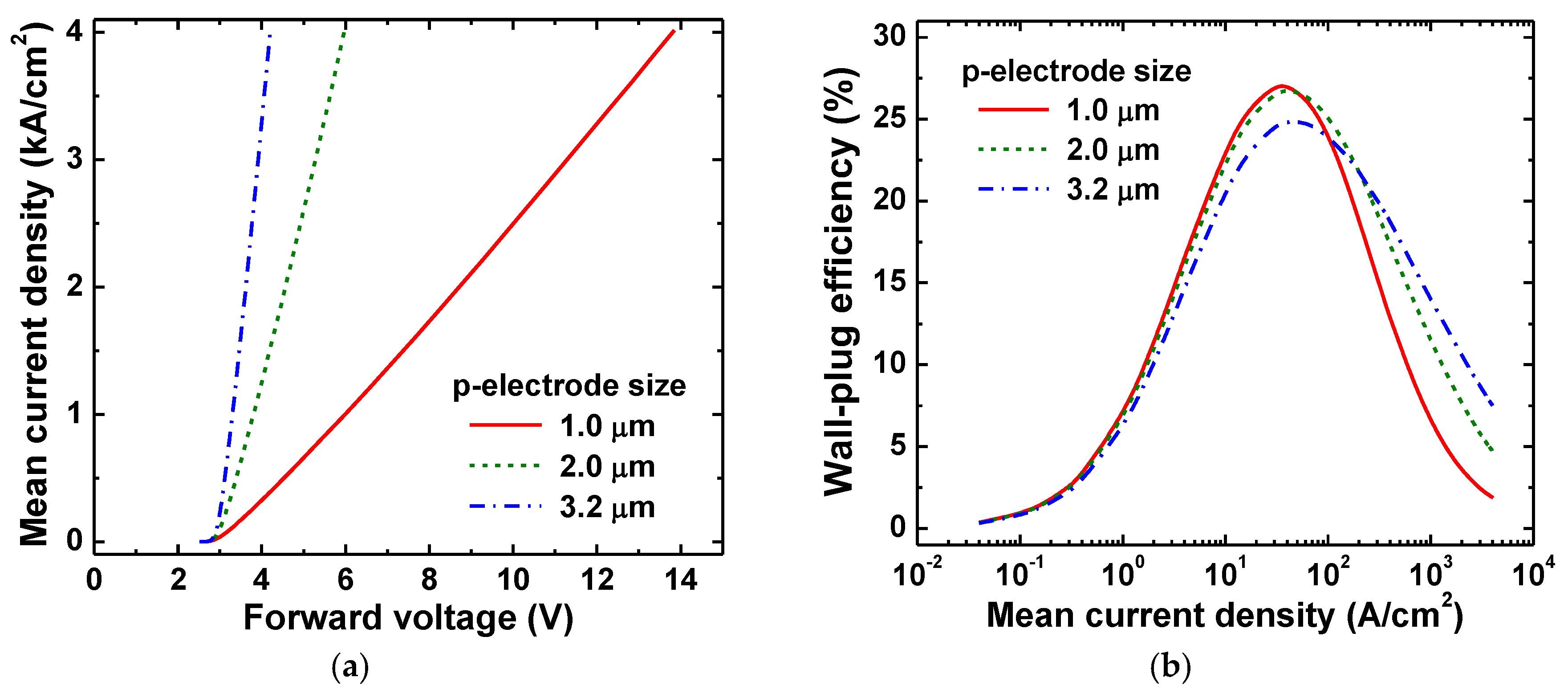
The μ-LED chip design considered in our study utilizes a small (
dp = 1.0 μm) p-electrode aimed at suppression of surface recombination by localization of current far from the active region edges. However, this results in a high specific series resistance of the μ-LED leading, eventually, to a lower WPE of the device. In order to understand whether it is possible to optimize the p-electrode dimensions, we have simulated characteristics of μ-LEDs with
dp = 2.0 μm and 3.2 μm. The most important results of the simulations are shown in
Figure 9.
Current density–voltage characteristics of the μ-LEDs with different p-electrode dimensions are compared in
Figure 9a. Increasing the lateral size of the p-electrode, from 1.0 μm to 3.2 μm, results in a dramatic improvement of the series resistance, from 2.71 mΩ·cm
2 to 0.33 mΩ·cm
2. Comparison of WPEs of the μ-LEDs, given in
Figure 9b, shows the following trends. First, the current density corresponding to WPE peak is shifted to higher values, and the peak WPE lowers at larger
dp, which is evidence for higher carrier losses for surface recombination. On the other hand, high-current WPE grows when
dp is enlarged. The latter effect can be explained by reduction of the μ-LED series resistance at larger
dp, thus lowering the operating voltage of the device. Hence, the optimal p-electrode dimensions depend on desirable μ-LED operation conditions. If the device is assigned for operation at peak WPE, then the use of small p-electrode is preferable. By contrast, high-current operation of the μ-LED requires utilizing larger p-electrode sizes. In particular, μ-LEDs with
dp = 3.2 μm are predicted to have WPE higher than in the case of
dp = 1.0 μm, by a factor of two, at 1 kA/cm
2 (see
Figure 9b).
Let us now discuss the roles of current crowding and surface recombination in operation of μ-LEDs. There is a common opinion that current crowding is not important in such small devices as μ-LEDs. Our simulations, comparing μ-LEDs with 5 × 5 μm
2 and 20 × 20 μm
2 active regions, show that this is not the case. This can be clearly seen, in particular, from
Figure 7, demonstrating essentially different LEE dependences on the current density for small and large μ-LEDs. Since the dependence originates from localization of the injected carriers under poorly reflective p-electrode enhanced with current, this effect can be unambiguously attributed to different current crowding in small and large devices. Another signature of the valuable current crowding is different self-heating of small and large μ-LEDs at high current densities, producing a corresponding thermal droop of the emission efficiency (see
Figure 8b). Hence, current crowding still remains an important factor, which should be accounted for in further developments of efficient μ-LEDs.
Our simulations were carried out with the surface recombination velocity
VS = 7.5 × 10
3 cm/s, obtained in [
22] for vertical side walls of the mesa likely formed by non-polar facets of wurtzite crystal. On the other hand, the use of small angles,
θ, of the facet inclination, which is beneficial for high LEE, may alter the surface recombination velocity. Indirect evidence for this is a large scatter in the data on
VS in InGaN and GaN, reported for various crystal orientations (see [
21] for a more detailed literature review on this issue). Therefore, experimental investigations into the crystal orientation dependence of surface recombination velocity are quite desirable for future developments of μ-LEDs. If the dependence of
VS on the orientation of the active region facets is found to be strong enough, the proper choice of the mesa-facet orientation/inclination may become an additional degree of freedom for optimization of μ-LEDs with embedded micro-reflectors.
In this study, we have tested, successfully, a novel approach to μ-LED simulation, utilizing the temperature-dependent characterization of large-size devices as the input data. The approach uses quite limited information on the operation of LED structure (see
Section 2.1). Due to the current lack of reliable experimental data and theoretical results on temperature-dependent recombination coefficients, the above approach becomes advantageous over the detailed simulations of LED structures from the predictability point of view. Operating with a limited number of integral parameters, it is not even required to know a particular LED structure. On the other hand, there are some limitations on the use of the approach. Based on the ABC-model, the approach fails in prediction of IQE of red AlInGaP LEDs, as the high-current efficiency droop in those devices originates from electron leakage to p-side of the LED structure, rather than from Auger recombination assumed in the ABC-model. In the case of true-green InGaN-based LEDs, a more complex model should be applied, in order to approximate, properly, the IQE dependence on the current density and temperature [
27].
5. Summary
In this study, a novel approach to LED simulations is suggested, utilizing temperature-dependent characterization of large-size devices as the input data. The approach has been applied to study the effects of shaping the blue μ-LED dice, aimed at increasing LEE and improving their overall efficiency.
Flip-chip blue μ-LED dice with truncated-pyramid shape and various inclinations of the mesa facets considered in this study, are compatible with μ-LED operation in high pixel-density arrays. After optimizing the thickness of insulating layer, LEE through the bottom surface of the μ-LED dice to air is found to vary non-monotonously with the facet inclination angle, from 15–20% up to 54.4% (with the total LEE peak of 58.8%). The projected LEE of optimized μ-LEDs encapsulated with silicone, having a refractive index of 1.41, is 66.9% to bottom hemisphere and 79.8% in total, respectively. The latter values are higher than the experimental LEE of large-size LEDs having similar designs. The major channels of optical losses identified by ray tracing are incomplete light reflection from the Ag-based n-electrode and free-carrier absorption in the thick n-contact layer. Due to current crowding, leading to current localization under the poorly reflective Au-based p-electrode, LEE is found to decrease with the current density, even in the case of small-size devices.
Peak EQE of about 30% and wall-plug efficiency (WPE) of 27% for bottom emission to air is predicted to be achievable for the μ-LEDs of optimal design with 5 × 5 μm2 active region at the parameters borrowed from characterization of real large-size LEDs. At the peak efficiency, the carrier losses in μ-LEDs caused by surface recombination do not exceed 15–20%. For light extraction to silicone, the projected total EQE approaches 43% (37% for bottom emission), which is higher than experimental EQEs reported to date. These results show that shaping of the μ-LED dice is an effective way for improvement of their emission efficiency.
We have found that small p-contacts produce the major contribution to specific series resistance of small μ-LEDs, which is a general problem of such devices irrespective of their particular designs. A natural way for overcoming this problem, i.e., increasing the p-electrode dimensions, should be compromised with possible enhancement of surface recombination when non-equilibrium carriers are injected into the active region next to its edges. Optimization of the p-electrode configuration, accounting for the above factor, enables remarkable improvement of high-current WPE of the μ-LEDs. In particular, WPE of about 13%, at the current density of 1 kA/cm2 predicted for optimized design of the μ-LED with 5 × 5 μm2 active region, seems to be large enough for practical applications.


