1. Introduction
Photonic-crystal (PC) surface-emitting lasers (SELs) or PCSELs, utilizing band-edge effect of a two-dimensional (2D)-PC structure, possess the advantages of single-mode operation, high optical output, narrow beam divergence and excellent beam quality [
1,
2,
3,
4,
5]. The principle of operation is that light emissions from gain media propagate with zero group velocity and strongly couple with 2D-PCs to construct the cavity mode where in-plane distributed feedback (DFB) diffracts vertically [
1]. Moreover, the cavity mode is achieved over a large lasing area with single longitudinal and transverse mode oscillations.
As in-plane optical feedback diffracts both upward and downward, the intuitive approach to harvest light output is to reflect downward emissions by bottom distributed Bragg reflector (DBR). Prior publication of violet PCSELs with bottom GaN/AlN DBR claimed to have higher top-emission efficiency when lasing wavelengths are in the stopband of DBR [
2]. InGaAs quantum-well (QW) PCSELs of 986 nm were demonstrated at room temperature (RT) to have slope efficiency as high as 0.85 W/A with the introduction of bottom GaAs/AlGaAs DBR [
3].
GaAs-based In(Ga)As quantum-dot (QD) gain media are a novel and low-cost solution for near-infrared lasing emissions between 1.1 and 1.3 μm. Recently, we have demonstrated the first QD PCSELs of 1.3-μm range at RT both by optical pumping and through electrical injection [
4,
5]. In this work, we demonstrate optically pumped QD PCSELs with bottom GaAs/AlGaAs DBR. The lasing wavelengths cover broad emission range from 1194 nm to 1296 nm. The lasing characteristics of QD PCSELs are investigated in terms of gain-cavity detuning, as well as sub-cavity effect.
2. Materials and Methods
The wafer for PCSEL fabrication was based on intracavity-contacted vertical-cavity SEL (VCSEL) structure grown on semi-insulting GaAs substrate by molecular beam epitaxy [
6]. The design wavelength (λ) of original VCSEL is 1300 nm in vacuum. However, lasing emissions were not achieved for VCSEL devices because of possible gain deficiency associated with long-time high-temperature growth of top DBR.
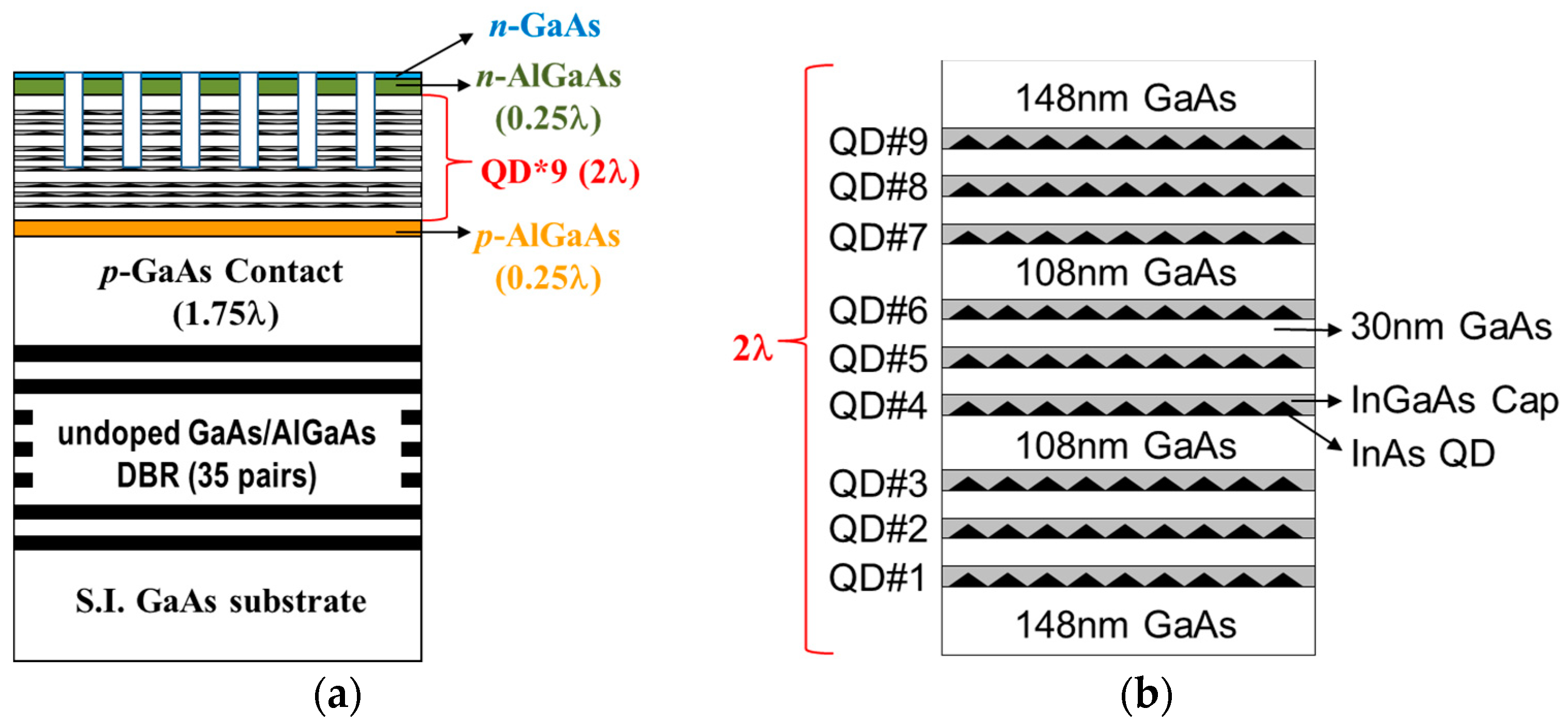
Figure 1a shows the schematic device structure of InAs QD PCSEL. The epitaxial layers started with undoped Al
0.9Ga
0.1As/GaAs bottom DBR of 35 pairs, followed by 1.75-λ p-doped GaAs contact layer, 0.25-λ p-doped high Al-content AlGaAs aperture layer, and proceeded with the active region shown in
Figure 1b. The active region, centered by GaAs in a 2-λ cavity, consisted of three groups of triple-stacked InAs QDs (labeled as QD#1 at the bottom to QD#9 at the top), which were capped by 5-nm In
0.15Ga
0.85As and spaced by 30-nm GaAs. Afterwards, another 0.25-λ but n-doped AlGaAs aperture layer was grown. Top DBR layers were etched by inductively coupled plasma (ICP) almost completely, but with remaining GaAs to a thickness of several nm.
The PCSELs were designed for the transverse electric (TE) mode in 2D square lattice operated at Γ band-edge. Before patterning the PCs, dielectric Si
3N
4 of 150 nm was deposited as hard mask by plasma enhanced chemical vapor deposition at 300 °C. PCs with circular shaped air holes were patterned on dielectric by e-beam lithography and ICP etcher. Again, 2D-PC structure was transferred into semiconductor layers by ICP. Since spreading and surface recombination of carriers were suppressed in QD gain media [
7], we followed the etch-through-QW structure, which adopted in GaN-based PCSELs with AlN/GaN DBR [
2], and incorporated etch-through-QD structure in our fabrication of 2D-PC holes.
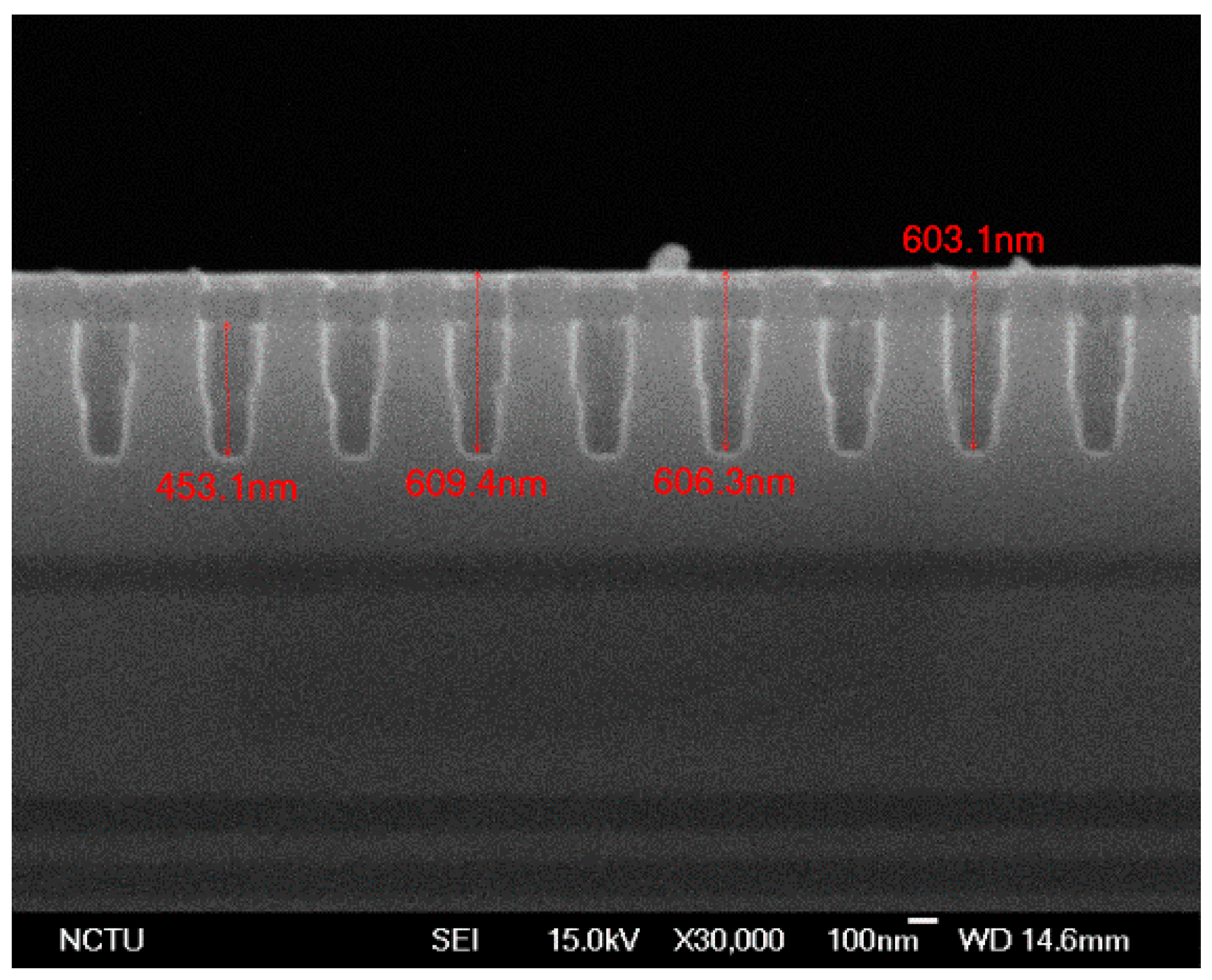
Figure 2 shows the cross-sectional image from the scanning electron microscope (SEM). The etch depth was about 600 nm. About six out of nine QD layers were punched through by PC holes.
Two lattice periods of 360 nm and 395 nm were investigated in this paper. The filling factor, defined as the area of unit lattice occupied by air hole, was as-designed to 10% according to our previous works [
4,
5]. Nevertheless, the filling factor disclosed in
Figure 2 was less than 10% at the bottom and more than 20% at the top. Strong coupling between QD and PC is expected; however, modal gain is also reduced by ~15% in filling factor. The fabricated devices, with a size of 300 × 300 μm
2, were optically pumped by a 1064-nm pulsed fiber laser with pulse width of 50 ns and repetition rate of 5 KHz. The measurement was temperature-controlled at RT of 20 °C by a thermoelectric cooler. The light emissions were collected by a grating monochromator equipped with a thermoelectric cooled InGaAs detector. The spectral resolution was as low as 0.05 nm.
3. Results and Discussion
After removing the top DBR, the sample without PC patterning was characterized at RT by photo-luminescence (PL) and reflectivity measurement. Both PL and reflectivity spectra are shown in
Figure 3. The ground-state (GS) and the excited-state (ES) wavelengths of InAs/InGaAs QDs cannot be easily resolved from the PL spectrum as it is subjected to sub-cavity modulation effects. The GS gain-peak wavelength was determined separately to be 1280–1300 nm, while the ES gain-peak wavelength was estimated to be 1200–1220 nm [
8].
The sub-cavity effect can be understood as a Fabry–Perot etalon established between bottom DBR and air-semiconductor interface [
9].
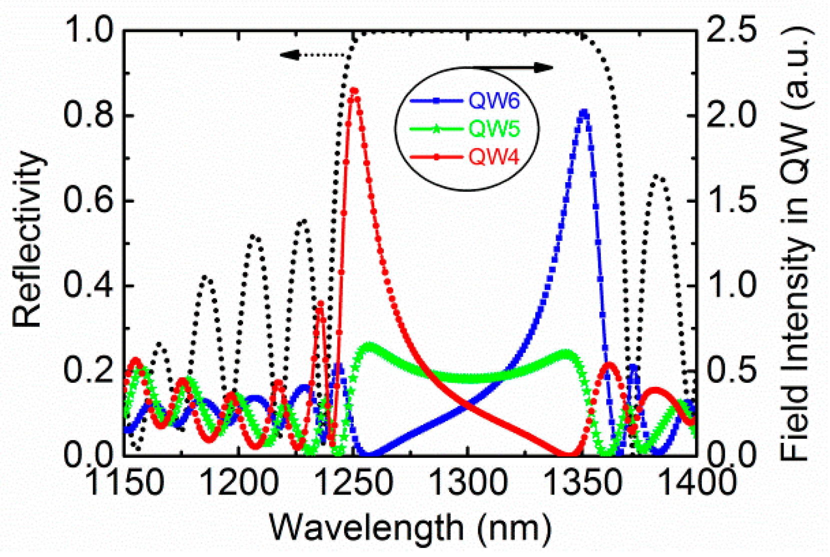
Figure 4 shows the simulated spectra of reflectivity as well as field intensity (|
E(λ)|
2) in central QD layers (QD#4, #5 and #6). The incident electric field is normalized to unity, i.e., |
Eincident(λ)|
2 = 1. The simulation is performed in one-dimensional (1D) and the effective gain is proportional to the product of actual gain and |
E(λ)|
2 at the points of multilayer QD location [
9]. The two resonant peaks in the field intensity spectra are within the stopband of the simulated reflectivity spectrum, which is nearly coincident with the measured one. Moreover, two resonant peaks around 1250 and 1350 nm in
Figure 4 give rise to two local peaks in the measured PL at around the same wavelengths. In addition, in the measured PL, the shoulder wavelength at 1285–1295 nm, with intensity diminished by out-of-resonance in sub-cavity, is credited to peak gain of GS emissions. The resolved GS wavelength is consistent with our separate measurement.
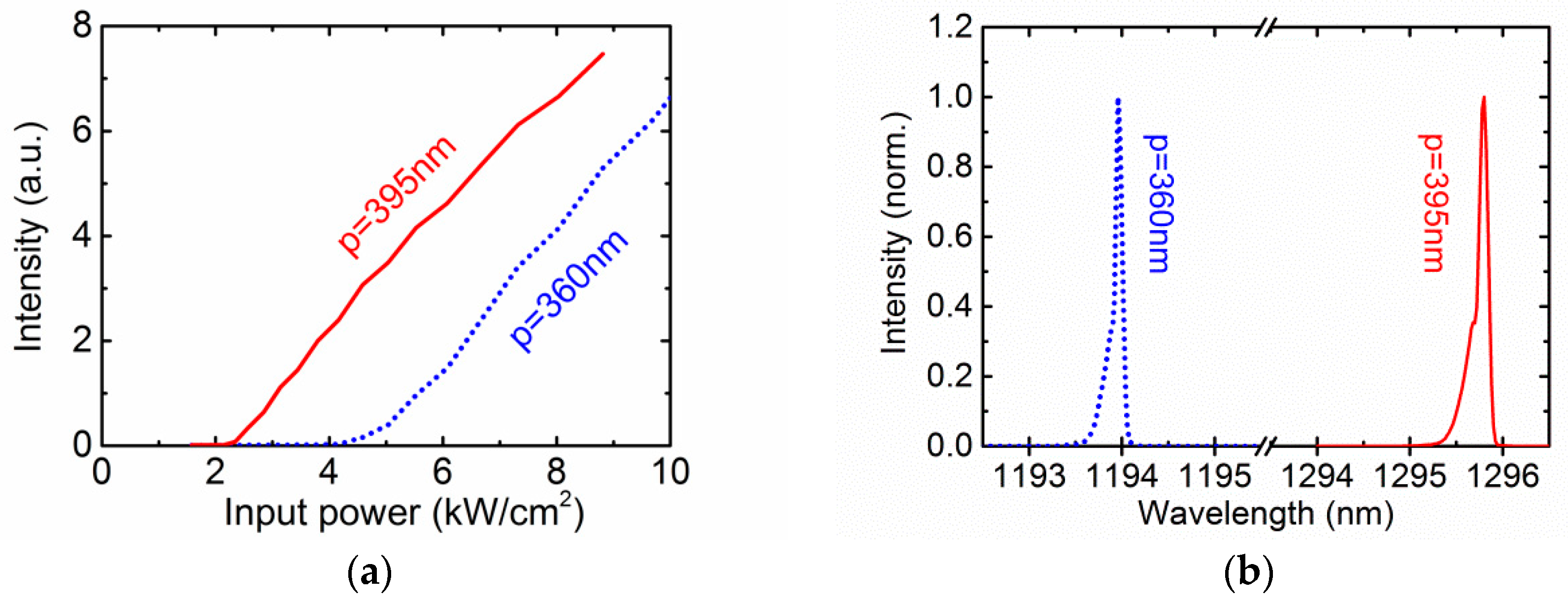
We have patterned two lattice periods of 360 nm and 395 nm. The RT light-light (
L-L) curves and lasing spectra of the QD PCSELs are shown in
Figure 5a,b respectively. For the 360-nm device, the threshold power density is about 4.2 kW/cm
2 and lasing wavelength is around 1194 nm. For the 395-nm device, the threshold power density is about 2.4 kW/cm
2 and lasing wavelength is around 1295.8 nm. The spectral full width of half maximum is less than 0.2 nm for both devices. Nonetheless, side mode is observed at the short-wavelength side of the main lasing mode. That is probably due to imperfection or non-uniformity of etched PC.
Our previous works revealed that threshold pumping densities of PCSELs are closely related to gain-cavity detuning between GS-QD gain-peak wavelength and PC cavity wavelength [
4,
5]. Here, the 360-nm PCSEL is positively detuned with detuning as huge as 100 nm; however, its threshold power density is less than two times that of 395-nm PCSEL, which is almost zero-detuned. This is because that lasing wavelength of 360-nm PCSEL falls within the optical gain bandwidth of ES emissions. In other words, 360-nm PCSEL is small positively detuned relative to ES gain-peak wavelength, which is more easily pumped than other wavelengths between GS and ES. The unique spectral gain characteristics of QDs should be taken into consideration in the interpretation of gain-cavity detuning.
Both devices in
Figure 5a were side by side with separation less than 1 mm so that their intensities can be compared without difficulty. The slope efficiencies in relative units are 1.29 and 1.17 for 360- and 395-nm devices, respectively. The 395-nm PCSEL in reflectivity stop-band of bottom DBR harvests no benefits from reflected downward emissions. The simulated field intensity spectra in
Figure 4 can provide the explanation. For PCSEL structure in
Figure 1, the resonant wavelength is neither 1300 nm for original VCSEL structure nor 1295 nm for 395-nm PCSEL. Instead, it is around 1250 nm or 1350 nm. Seen another way, the total thickness of the sub-cavity formed between bottom DBR and air-semiconductor interface is 4.25-λ, which creates almost completely destructive interference for lasing wavelength of 395-nm PCSEL. Therefore, the energies stored in QD multilayers for two lasing wavelengths of 360- and 395-nm devices are approximately equal, as shown in
Figure 4. As a result, the surface-emitting slope efficiencies for these two PCSELs are only comparable.
It was also reported that surface-emitting power is strongly dependent on vertical quality factor (
Qv), which was defined in Reference [
10]. The control of
Qv is done by adjusting the phase relation between upward and downward emissions from a PC cavity incorporated with bottom DBR [
3]. If the 0.25-λ n-AlGaAs aperture layer is removed in the modified structure, the 395-nm PCSELs are expected to exhibit higher slope efficiency as well as lower pumping threshold.
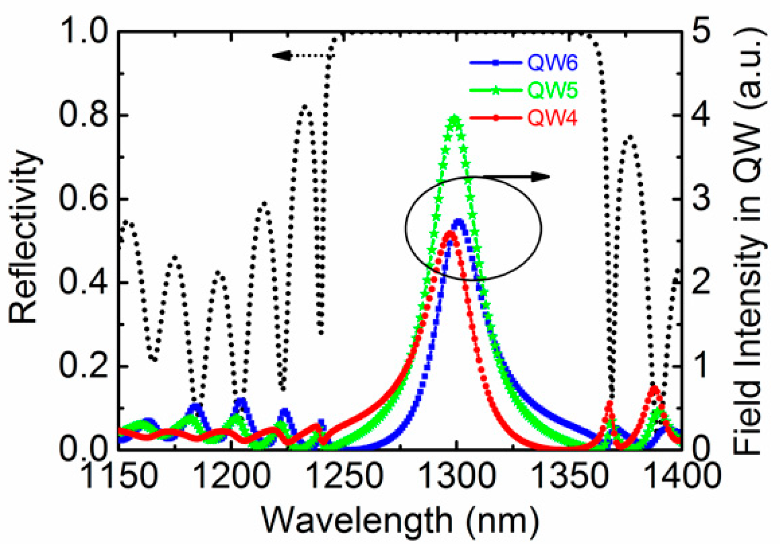
Figure 6 shows the simulated spectra of reflectivity as well as field intensity in QD layers for the modified structure. The lasing wavelength of 395-nm PCSEL is then in phase with the resonant wavelength of modified sub-cavity. As shown in
Figure 6, the energy stored in QD multilayers for 395-nm PCSEL is now several times higher than that for 360-nm PCSEL.

