Abstract
In this work, we introduce a totally vacuum-free cost-efficient crystalline silicon solar cells. Solar cells were fabricated based on low-cost techniques including spin coating, spray pyrolysis, and screen-printing. A best efficiency of 17.51% was achieved by non-vacuum process with a basic structure of <AI/p+/p−Si/n+/SiO2/TiO2/Ag> CZ-Si p-type solar cells. Short circuit current density (JSC) and open circuit voltage (VOC) of the best cell were measured as 38.1 mA·cm−2 and 596.2 mV, respectively with fill factor (FF) of 77.1%. Suns-Voc measurements were carried out and the detrimental effect of the series resistance on the performance was revealed. It is concluded that higher efficiencies are achievable by the improvements of the contacts and by utilizing good quality starting wafers.
1. Introduction
Solar energy is one of the most interested and practical alternative sources of energy against the conventional fossil fuels. Crystalline silicon based solar cells are dominant in the photovoltaic industry and comprise about 90% of solar cell production worldwide. Low cost is still one of the main goals for solar cell manufacturing while maintaining a stable high conversion efficiency. Utilized materials and processing techniques are the major components that need to be considered for cost reduction. A conventional p-type solar cell fabrication process is basically comprised of texturing, n-type emitter formation (phosphorus diffusion), bulk and surface passivation, anti-reflection coating (ARC), and back surface field and front contact formations by back/front metallization steps.
To form homogenous phosphorus-diffused emitters for p-type silicon solar cells, thermal diffusion of phosphorus oxychloride (POCl3) [1,2] is commonly utilized as a state-of-art method. Other than POCl3 diffusion, diluted orthophosphoric acid (H3PO4) by spray [3,4], sol-gel sources through spin-on deposition techniques [5], or screen-printing technique [6] can be some alternatives.
On the other hand, improving the absorption properties and reducing the optical losses in solar cells are the most important sequences in cell manufacturing to achieve high efficiencies. ARC films are commonly used on the surface of textured cells to reduce the reflectivity further and to improve the photo current which leads to improving the efficiency of the solar cell. SiNx films or SiNx based stack layers are commonly used in the commercial solar cells for ARC purposes with their effective antireflective behavior and good passivation effect [7,8]. However, its deposition technique of plasma-enhanced chemical vapor deposition (PECVD) [9,10] has some drawbacks, including the need for toxic and hazardous gases such as SiH4 and NH3 with vacuum processing for chemical vapor deposition operation, difficult handling, and high costs. Besides, the common use of vacuum processes for ARC formations for single junction crystalline silicon solar cells, especially heterojunction solar cells, basically relies on sequential delicate vacuum-processed applications [11]. Back and front metallization of silicon solar cells is conventionally carried out by a screen-printing method using Al and Ag based pastes, respectively.
Although, high efficiency solar cells greater than 20% including record efficiencies provide a good performance [11,12], they cannot demonstrate the feasibility for low-cost scale due to complex structures and long and costly fabrication processes. Therefore, the average efficiency of standard industrial cells still remains in the range of 15–20%. From this point of view, a lot of efforts have been devoted to developing low cost solar cells with new materials, cost effective processing, optimized structures and new device architectures.
In order to meet industrial requirements with simple low-cost technologies with high throughput, cost-effective methods need to be investigated and adapted to the solar cell manufacturing processes. When considering that the cost per unit area can be very high for high efficiency modules, the importance of such approaches becomes prominent. As an alternative to the vacuum-processed SiNx ARC, TiO2 and its multilayer structures have been introduced in earlier decades [13,14,15], due to its good optical properties and high refractive index to enhance the light absorption capability of silicon solar cells. In our previous studies, TiO2, Al2O3/TiO2, and ZrO2/TiO2 ARC films were introduced [16,17,18] based on spin coating and spray deposition techniques. By adaptation of such simple processing techniques—including spin coating, spray deposition, and screen printing methods—into the cell manufacturing process with proper materials, high efficiency solar cells that can be compatible with their commercial counter parts. Based on these considerations, the importance of a vacuum-free process on solar cell manufacturing can draw attention for future development of solar cells.
This paper determines the ground for high efficiency totally vacuum-free, low cost crystalline silicon solar cell manufacturing process and applications using cost effective methods. The approach in this paper can assist in lowering the efficiency gap between the commercial cell and a high-quality laboratory cell owing to the easily reachable and simple technologies.
2. Experimental
For the fabrication of c-Si solar cells, 25 × 25 mm p-type CZ-Si wafers were used, which were cut from 6-inch wafers (thickness: 400 μm; resistivity: ~5 Ωcm). At first, all wafers were etched for 5 min in acidic solution containing HF:HNO3 (1:5 vol %) for saw damage etching. For surface-textured Si solar cells, alkaline texturing was performed in KOH (5.19 g) solution in H2O (100 mL) with Alka-Tex (0.28 mL, GP Solar, Konstanz, Germany) at 80 °C for 30 min. Silicon wafers then were dipped into the 20% diluted HF for 10 min and rinsed in distilled water. Afterwards, RCA cleaning [19,20] was carried out to remove contaminant particles on the surface of the wafers by using a NH3/H2O2/H2O (1:1:5 vol %) solution, for 60 min at 80 °C. After the removal of the natural oxide films by 20% HF, a mixed solution of HCl/H2O2/H2O (1:1:5 vol %) was used to remove metallic contaminants and mobile ions on the surface by dipping the wafers for 60 min at 80 °C. POCl3 diffusion was performed at 880 °C for 40 min with 0.2 L/min N2 flow, in order to obtain n+ emitter. After the diffusion, wafers were successively rinsed by dipping in 10% HF and pure water for 5 min to remove phosphorus silica glass. Sheet resistances of the phosphorus diffused wafers were resulted in a range of 40–45 Ω/sq. Thermal oxidation was carried out by O2/H2O bubbling at 800 °C for 10 min.
TiO2 ARC films were formed on the surface of wafers by spray pyrolysis deposition technique with a glass atomizer using precursor solutions. Deposited film thicknesses were mainly controlled by the amount of sprayed precursor solutions. The TiO2 precursor solution was prepared by titanium bis isopropoxidebisacethylacetone (TAA) (prepared by mixing titanium (VI) isopropoxide and acetylacetone in a 1:2 mole ratio) to ethanol (1:10 vol %). For the deposition of TiO2 films, silicon wafers were set on a hot plate heated at deposition temperature of 450 °C and 475 °C, respectively. According to the optimizations in our prior studies [17,18], TiO2 films were formed to a 90 nm thickness using 100 mL precursor solution.
Front and back contacts were formed by screen-printing Ag and Al, respectively. The printed metal pastes were dried at 125 °C for around 5 min and then co-fired at 770 °C for 1 min. Finally, each edge of the wafer was cut with 2 mm width for the edge isolation. The resulting size of the samples used for photocurrent voltage (I-V) measurements was around 20 mm × 20 mm.
The sheet resistances of the wafers were measured by a four-point-probe method (using Loresta-EP MCP-T36 tool by Mitsubishi Chemical Corp., Chiyoda, Tokyo, Japan). For the (I-V) measurements, an AM1.5 solar simulator (with a 500 W Xe lamp, YSS-80A, Yamashita Denso, Japan) calibrated to 100 mW·cm−2 using a reference silicon photodiode (Bunkou Keiki, Japan) was utilized.
3. Results and Discussion
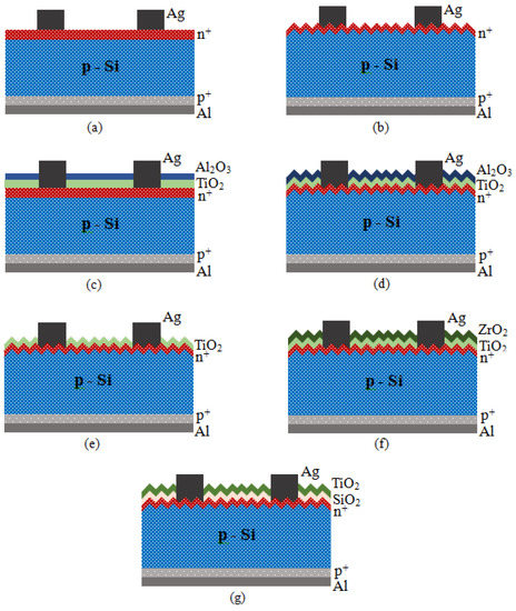
In our recent studies, we have been introduced TiO2, Al2O3, and ZrO2 single or double layers based on spin coating or spray pyrolysis methods [16,17,18]. Those results were remarkable to suggest low temperature and non-vacuum processed ARC film as an alternative to mainstream silicon nitrate based films. Figure 1 presents the schematics of solar cells fabricated in our previous works and the one introduced in current work.

Figure 1.
Schematics of solar cell structures fabricated with non-vacuum process techniques with various surface structures and with various ARC films, (a) <AI/p+/p−Si/n+/Ag> with flat surface, (b) <AI/p+/p−Si/n+/Ag> with textured surface, (c) <AI/p+/p−Si/n+/TiO2/AI2O3/Ag> with flat surface, (d) <AI/p+/p−Si/n+/TiO2/AI2O3/Ag> with textured surface, (e) <AI/p+/p−Si/n+/TiO2/Ag> with textured surface, (f) <AI/p+/p−Si/n+/TiO2/ZrO2/Ag> with textured surface, (g) <AI/p+/p−Si/n+/SiO2/TiO2/Ag> with textured surface.
Electrical characteristics of fabricated cells with flat or textured surfaces are summarized in Table 1. Although it was shown that the vacuum-less processed TiO2, Al2O3, and ZrO2 based ARC layers were promising, the power conversion efficiencies were limited to around 16%. The main drawback of those vacuum-less processed solar cells was the insufficient front surface passivation, even though the average reflectance (300–1100 nm) of the textured silicon surface with ARC could be reduced significantly down to below 7% [16,17,18]. In this study, SiO2 layer formation upon thermal oxidation was performed by O2/H2O bubbling and a SiO2/TiO2 stack layer was formed with spray deposited TiO2 film for further improvements.

Table 1.
Electrical characteristics of vacuum-less processed crystalline silicon solar cells. A summary including our previous work.
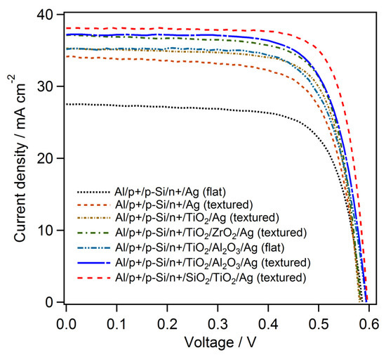
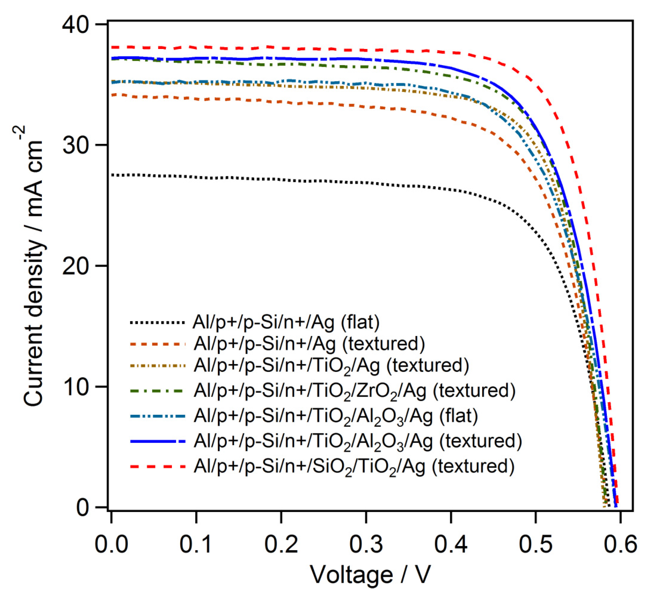
Conversion efficiency of the simplest cell structure of <AI/p+/p−Si/n+/Ag (flat surface)> without any surface texturing has an average cell efficiency of 10.2% with the JSC of 27.75 mA·cm−2. JSC was improved up to 33.47 mA·cm−2 on textured surface solar cells <AI/p+/p−Si/n+/Ag (textured surface)> and average conversion efficiency reaches 13.8%. An increase of more than 3% efficiency is due to the improvement of light collection on textured surface and low series resistance which leads higher FF.
It is known that an effective ARC layer into the solar cell structure would boost the efficiency, owing to the better light trapping. In our previous study [18], vacuum-less processed solar cells with TiO2 single layer ARC deposited by spray pyrolysis (<AI/p+/p−Si/n+/TiO2/Ag>) achieved JSC of 35.3 mA·cm−2 where the efficiency was 15.2%. Further improvement of JSC with double ARC established by spin coating ZrO2 film formed on spray deposited TiO2 film could be obtained in that work as 37.2 mA·cm−2 with a conversion efficiency of 15.9% (<AI/p+/p−Si/n+/TiO2/ZrO2/Ag>). Additionally, we introduced <AI/p+/p−Si/n+/TiO2/AI2O3/Ag> structured solar cells with TiO2/AI2O3 double ARC films [16]. Spray deposited AI2O3 films coated on spray deposited TiO2 films to finalize <AI/p+/p−Si/n+/TiO2/AI2O3/Ag> structured solar cells either with flat or textured surfaces. The average efficiency of 15.5% was achieved with JSC of 37 mA·cm−2 on solar cells with textured surface that are 1.1% and 2.5 mA·cm−2 greater than that of the values for cells with a flat surface. The light trapping effect of textured surfaces was observed clearly for each type of fabricated solar cells when compared to those of the cells with flat front surface. Additionally, these results show that efficiencies could be increased by the application of spin coated or spray deposited TiO2, ZrO2, and AI2O3 based ARC films. However, the highest efficiency was observed at around 16%.
Finally, a record efficiency of 17.51% (average of three samples: 17.22%) was obtained in this work with totally non-vacuum processed <AI/p+/p−Si/n+/SiO2/TiO2/Ag> structured solar cells with textured surface. Thermally evaporated SiO2/spray deposited TiO2 stack was used as passivation/ARC layer and JSC of solar cells reached up to 38.1 mA·cm−2. VOC and FF were measured as 596.2 mV (average of three samples: 591.9 mV) and 77.1% (average of three samples: 76.3%), respectively. I–V curves of the best cells of each structure are given in Figure 2.

Figure 2.
I–V curve of the fabricated solar cells by each vacuum-less process.
In order to realize the limiting factors on the fabricated solar cells, further characterizations were carried out by Suns-Voc analysis tool. The Suns-Voc analysis tool is an effective characterization method to estimate the potential performance of the wafers being processed for a finalized solar cell [21]. It allows monitoring each step of the solar cell fabrication process, including post-phosphorus diffusion, ARC formation, and as well as after Ag and Al contact firings in order to optimize emitter layers and potential shunting and to observe the effect of series resistance to the conversion efficiency.
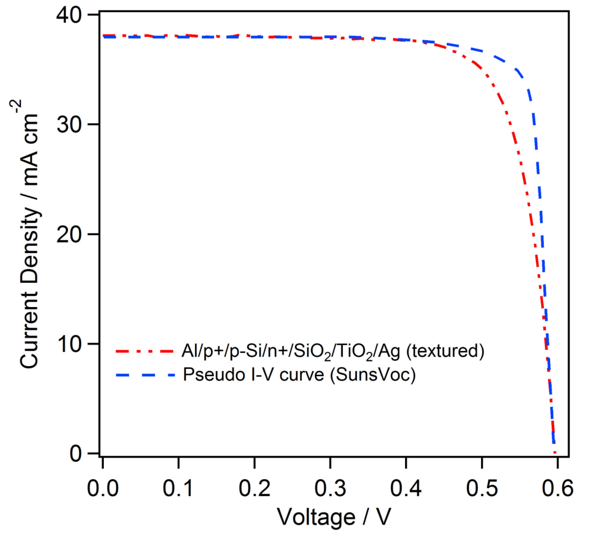
Suns-Voc measurements were carried out for the best cell of <AI/p+/p−Si/n+/SiO2/TiO2/Ag (textured surface)> structured solar cells to yield the pseudo-efficiency (pEff) without the effect of series resistance, pseudo FF (pFF). The comparison of the actually measured I–V curve of the cell and the fitted I–V curve of Suns-Voc is given in Figure 3.

Figure 3.
Measured I–V curve of the best cell compared with the pseudo I–V curve measured by Suns-Voc.
The pseudo I–V curve obtained from the Suns-Voc measurement provides a pEff of 18.5% with pFF of 81.6%, greater than that of the actually measured values of 17.52% and 77.1%, respectively. The difference is due to the elimination of series resistance during the Suns-Voc measurement. Moreover, considering the maximum potential efficiency of the regarding cell as 18.5%, one can conclude that, besides the resistive losses, the limited performance of the fabricated cells can be attributed to the low VOC which can be due to the recombination losses in the solar cell because of the poor initial bulk quality and inadequate control of the interface of the formed oxide layer with the silicon bulk. These results indicate that higher efficiencies are achievable by the improvements of the contacts and utilizing good quality starting wafers.
On the other hand, some of previous studies and onsite experiences may encourage doubt about using TiO2 based ARCs [22,23]. These investigations showed almost linear degradation of JSC by UV exposure dose for silicon solar cell modules which in some cases caused color changes in ethylene-vinyl acetate (EVA) as well. Although it was initially thought that the EVA coloring was the main reason for that degradation, then it turned out that the most likely reason is the UV exposure [24,25]. In the case that this effect is proved to be detrimental, the solution could be blocking the UV exposure while absorbing the light and using colored glass filters to limit the UV absorption. However, this content is still unknown and on investigation.
4. Conclusions
The aim of this study was to introduce high efficient vacuum-free processed crystalline silicon solar cells. It was shown that a simple structure of CZ-Si p-type solar cell (<AI/p+/p−Si/n+/SiO2/TiO2/Ag>) including a spray deposited TiO2 ARC reaches an efficiency of 17.52% where the average efficiency of three samples was 17.22%. The JSC of the best solar cell reached up to 38.1 mA·cm−2. The VOC and FF of the best cell were measured as 596.2 mV and 77.1%, respectively. Results of the study make a good contribution to the development of cost-effective vacuum-free silicon solar cells. Further investigation and experimentation needs to be carried out for further improvements.
Acknowledgments
This work had been supported by Daiwa Sangyo Co., Ltd., Japan.
Author Contributions
T.H. and S.I. conceived and designed the experiments; A.U., H.K., T.I., and H.F. performed the experiments; A.U. and H.K. analyzed the data; A.U. contributed reagents/materials/analysis tools; A.U. wrote the paper.
Conflicts of Interest
The authors declare no conflict of interest.
References
- Florakis, A.; Janssens, T.; Posthuma, N.; Delmotte, J.; Douhard, B.; Poortmans, J.; Vandervorst, W. Simulation of the phosphorus profiles in a c-Si solar cellfabricated using POCl3 diffusion or ion implantation and annealing. Energy Procedia 2013, 38, 263–269. [Google Scholar] [CrossRef]
- Urrejola, E.; Peter, K.; Soiland, A.; Enebakk, E. POCl3 diffusion with in-situ SiO2 barrier for selective emitter multicrystalline solar grade silicon solar cells. In Proceedings of the 24th European Photovoltaic Solar Energy Conference, Hamburg, Germany, 21–25 September 2009. [Google Scholar]
- Bouhafs, D.; Moussi, A.; Boumaour, M.; Abaïdia, S.E.K.; Mahiou, L. N+ silicon solar cells emitters realized using phosphoric acid as doping source in a spray process. Thin Solid Films 2006, 510, 325–328. [Google Scholar] [CrossRef]
- Voyer, C.; Biro, D.; Wagner, K.; Benick, J.; Preu, R. Fabrication of Textured Solar Cells Using Sprayed Phosphoric Acid as the Dopant Source for the in-Line Emitter Diffusion. In Proceedings of the 21st European Photovoltaic Solar Energy Conference, Dresden, Germany, 4–8 September 2006; p. 1157. [Google Scholar]
- Lee, Y.-Y.; Ho, W.-J.; Syu, J.-K.; Lai, Q.-R.; Yu, C.-M. 17.9% Efficiency Silicon Solar Cells by Using Spin-on Films Processes. In Proceedings of the PIERS, Progress in Electromagnetics Research Symposium, Suzhou, China, 12–16 September 2011. [Google Scholar]
- Uzum, A.; Hamdi, A.; Nagashima, S.; Suzuki, S.; Suzuki, H.; Yoshiba, S.; Dhamrin, M.; Kamisako, K.; Sato, H.; Katsuma, K.; et al. Selective emitter formation processusing single screen-printed phosphorus diffusion source. Sol. Energy Mater. Sol. Cells 2013, 109, 288–293. [Google Scholar] [CrossRef]
- Richards, B.S. Comparison of TiO2 and other dielectric coatings for buried-contact solar cells: A review. Progress Photovolt. Res. Appl. 2004, 12, 253–281. [Google Scholar] [CrossRef]
- Dekkers, H.F.; Beaucarne, G.; Hiller, M.; Charifi, H.; Slaoui, A. Molecular hydrogen formation in hydrogenated silicon nitride. Appl. Phys. Lett. 2006, 89, 211914. [Google Scholar] [CrossRef]
- Aberle, A.; Hezel, R. Progress in low-temperature surface passivation of silicon solar cells using remote-plasma silicon nitride. Progress Photovolt. 1997, 5, 29–50. [Google Scholar] [CrossRef]
- Wan, Y.; McIntosh, K.R.; Thomson, A.F. Characterisation and optimisation of PECVD SiNx as an antireflection coating and passivation layer for silicon solar cells. AIP Adv. 2013, 3, 032113. [Google Scholar] [CrossRef]
- Masuko, K.; Shigematsu, M.; Hashiguchi, T.; Fujishima, D.; Kai, M.; Yoshimura, N.; Yamaguchi, T.; Ichihashi, Y.; Mishima, T.; Matsubara, N.; et al. Achievement of more than 25% conversion efficiency with crystalline silicon heterojunction solar cell. IEEE J. Photovolt. 2014, 4, 1433–1435. [Google Scholar] [CrossRef]
- Deng, W.; Chen, D.; Xiong, Z.; Verlinden, P.J.; Dong, J.; Ye, F.; Li, H.; Zhu, H.; Zhong, M.; Yang, Y.; et al. 20.8% PERC Solar Cell on 156 mm × 156 mm P-Type Multicrystalline Silicon Substrate. IEEE J. Photovolt. 2016, 6, 3–9. [Google Scholar] [CrossRef]
- Brinker, C.J.; Harrington, M.S. Sol-Gel derived antireflective coatings for silicon. Sol. Energy Mater. 1981, 5, 159–172. [Google Scholar] [CrossRef]
- Richards, B.S. Single-Material TiO2 double-layer antireflection coatings. Sol. Energy Mater. Sol. Cells 2003, 79, 369–390. [Google Scholar] [CrossRef]
- Lien, S.Y.; Wu, D.S.; Yeh, W.C.; Liu, J.C. Tri-layer antireflection coatings (SiO2/SiO2–TiO2/TiO2) for silicon solar cells using a sol–gel technique. Sol. Energy Mater. Sol. Cells 2006, 90, 2710–2719. [Google Scholar] [CrossRef]
- Kanda, H.; Uzum, A.; Harano, N.; Yoshinaga, S.; Ishikawa, Y.; Uraoka, Y.; Fukui, H.; Harada, T.; Ito, S. Al2O3/TiO2 double layer anti-reflection coating film for crystalline silicon solar cells formed by spray pyrolysis. Energy Sci. Eng. 2016, 4, 269–276. [Google Scholar] [CrossRef]
- Uzum, A.; Kuriyama, M.; Kanda, H.; Kimura, Y.; Tanimoto, K.; Ito, S. Non-Vacuum Processed Polymer Composite Antireflection Coating Films for Silicon Solar Cells. Energies 2016, 9, 633. [Google Scholar] [CrossRef]
- Uzum, A.; Kuriyama, M.; Kanda, H.; Kimura, Y.; Tanimoto, K.; Fukui, H.; Izumi, T.; Harada, T.; Ito, S. Sprayed and Spin-Coated Multilayer Antireflection Coating Films for Nonvacuum Processed Crystalline Silicon Solar Cells. Int. J. Photoenergy 2017, 2017, 5. [Google Scholar] [CrossRef]
- Reinhardt, K.; Kern, W. (Eds.) Handbook of Silicon Wafer Cleaning Technology, 2nd ed.; William Andrew Publishing: Norwich, NY, USA, 2008. [Google Scholar]
- Koch, W. Properties and uses of ethylcellulose. Ind. Eng. Chem. 1937, 29, 687–690. [Google Scholar] [CrossRef]
- Sinton, R.A.; Cuevas, A. A Quasi-Steady-State Open-Circuit Voltage Method for Solar Cell Characterization. In Proceedings of the 16th European Photovoltaic Solar Energy Conference, Glaskow, UK, 1–5 May 2000; pp. 1152–1155. [Google Scholar]
- Wenger, H.J.; Schaefer, J.; Rosenthal, A.; Hammond, B.; Schlueter, L. Decline of the Carrisa Plains PV Power Plant: The impact of concentrating sunlight on flat plates. In Proceedings of the 22nd IEEE Photovoltaic Specialists Conference, Las Vegas, NV, USA, 7–11 October 1991; pp. 586–592. [Google Scholar]
- Rosenthal, A.L.; Lane, C.G. Field Test Results for the 6 MW Carrizo Solar Photovoltaic Power Plant. Sol. Cells 1991, 30, 563–571. [Google Scholar] [CrossRef]
- Osterwald, C.R.; Pruett, J.; Moriarty, T. Crystalline silicon short-circuit current degradation study: Initial results. In Proceedings of the 31st IEEE Photovoltaic Specialists Conference, Lake Buena Vista, FL, USA, 3–7 January 2005; pp. 1335–1338. [Google Scholar]
- Osterwald, C.R.; Anderberg, A.; Rummel, S.; Ottoson, L. Degradation Analysis of Weathered Crystalline Silicon PV Modules. In Proceedings of the 29th IEEE PV Specialists Conference, Piscataway, NJ, USA, 20–24 May 2002; pp. 1392–1395. [Google Scholar]
© 2017 by the authors. Licensee MDPI, Basel, Switzerland. This article is an open access article distributed under the terms and conditions of the Creative Commons Attribution (CC BY) license (http://creativecommons.org/licenses/by/4.0/).


