1. Introduction
Rectangular microcavities in silicon-on-insulator (SOI) have attracted research attention because of their diverse applications ranging from optical filters [
1] to refractive index sensors [
2] due to their multimode resonant nature. Regarding optical filters, the most common micro resonator shapes have been the ring resonator [
3,
4] and disk resonator [
5,
6] due to their high
Q value of up to 10
7 with radius of 2.45 mm [
7] and their feasibility to fabricate them with different materials [
8,
9,
10]. Nevertheless, a shape that has a great potential is the rectangular resonator because the advantage of using them as filters is their smaller footprint requirement compared to the demonstrated ring resonators [
7]. Also, rectangular resonators are ideal candidates for sensing applications as they maximize the footprint efficiency while providing a significant sensing area in comparison with photonic crystals [
11]. Another advantage is the relaxation of the fabrication process because precise periods or gaps are not required as in [
12]. However, their intrinsic resonant characteristics lead to a moderate
Q-value of 4000 [
13], and several attempts have been made to enhance it by cutting the corners [
14] or by using different types of polygons such as triangles [
15], hexagons [
16,
17], octagons [
18], and deformed versions of these shapes [
19,
20]. Some of these approaches have not been fabricated and experimentally characterized [
21], while others have been fabricated in silica [
22], silicon nitride [
20], and the coupling has been performed by bulk optics such as prism coupling [
23]. In [
13], the authors were partially successful in demonstrating a square add-drop filter in silicon, but no power was detected in the drop waveguide mainly because of their high losses due to using very narrow waveguides. In this paper, we experimentally demonstrate the multimode optical resonance characteristics of large rectangular cavities in SOI in the transmitted and drop port and optimize the design parameters to enhance the
Q value to provide a way to filter and route optical signals. We present the design, fabrication, and characterization of three different sizes of rectangular microresonators in an add-drop filter configuration, as well as in a novel configuration of eight ports to validate the symmetry of the device and show, for the first time to our knowledge, selective mode coupling and a high
Q value of 13,000.
The following sections are organized as follows. First, in
Section 2, the device is analyzed with two-dimensional finite difference time domain (2D-FDTD) simulations. Then, the fabrication procedures are described and the experimental setup is introduced in
Section 3. In
Section 4, we show the experimental results of the optical characterization of the devices and are in good agreement with our simulations. Also, in this section, we demonstrate the effects of the gap and coupling length between the waveguides and resonator for transverse electric (TE) and transverse magnetic (TM) polarized light and find the optimum configuration to achieve the highest
Q value. At the end of this same section, we present the eight-port device and the experimental validation of the symmetry of the system. Finally, in
Section 5, we conclude the paper.
2. Design and Analysis
The basic add-drop filter configuration of the rectangular microresonator that is evanescently coupled to planar waveguides is illustrated in
Figure 1. It consists of two parallel waveguides of width denoted as
WGW with a rectangular resonator of size
L ×
W placed between them, separated by an air gap
g. The input wave travels in the top waveguide with a
k-vector
kwg and evanescently couples to the microresonator with a coupling coefficient κ, and when in resonance, there is a simultaneous increase in optical power in the drop ports and a decrease in power in the transmitted port. The nature and characteristics of the electromagnetic field profile inside the cavity at resonant wavelengths have been previously studied by mode expansion modeling [
24], coupled guided mode [
25], exact analytical solutions [
26,
27], and FDTD simulations [
28,
29].
All the methods have found that a standing wave appears inside the resonator, having different numbers of field extrema in the
z and
x directions, denoted by (
mz,
mx). Degenerate modes have the same resonant wavelength, but different angle
θ of the
k-vector in the resonator. These modes are (
mz,
mx) and (
mx,
mz). As the field inside the cavity is a standing wave, it can be analytically described by a superposition of sine waves in the
z and
x directions, as given by [
29].
where
A is the field amplitude,
ω is the mode angular frequency,
B is the amplitude of (
mx,
mz) mode, and
δ is the relative phase between degenerate modes.
Now, when evanescently coupling to a resonator larger than the wavelength, ray optics can also be used to describe the characteristics instead of a rigorous mode analysis. The wave travelling in the waveguide with a
kwg vector with angle
φ will couple to the resonator and bounce four times around the cavity with an angle
θ. When the bouncing wave inside the cavity matches the waveguide front after the bounces, the system resonates and these modes are called whispering-gallery like-modes (WGM). Only the modes that bounce with angles that meet the total internal reflection (TIR) confinement will be trapped inside, and from these modes, the ones that have an angle similar to
φ will preferably couple to the waveguide [
29]. A WGM that has a four-bounce travel around the cavity with 45° reflection angles has a Free Spectral Range (
FSR) given by
.
It is evident from the design that the size of the resonator sets the
FSR, and the coupling coefficient
κ plays a significant role in the amount of power coupled to the resonator, affecting the
Q value of the resonances. The coupling coefficient is related to three factors, the losses of the system denoted by
A, the
Q factor, and the
FSR. It can be experimentally extracted by [
13].
It is our interest to experimentally demonstrate the multimode behavior of the cavity, preferential mode coupling to a single mode waveguide and to optimize the parameters of the system to obtain the highest possible Q value.
In order to design the device and analyze the results, we employ a commercial FDTD software [
30] to simulate a device as the one shown in
Figure 1. Our main design consists of a rectangle of size
L = 20 μm,
W = 10 μm,
g = 160 nm, and
WGW = 450 nm for TE-polarization. We chose this size keeping in mind the trade-off between higher
Q values at the cost of footprint size as stated in Equation (2). Small square sizes of
L = 2 μm [
14] and large sizes of
L = 50 μm [
13] have been previously reported but it is the first time a rectangular shape of this size is studied. As it will be shown, rectangular resonators allow for more power to be coupled to the cavity that enhances the
Q factor. The gap size and waveguide widths are chosen so they can be readily achieved by electron beam lithography (EBL) and are compatible with other photonic devices for single mode operation. Our minimum gap size partially limited by our fabrication technology is in the order of 150 nm, so this is the closest we can separate the bus waveguide from the cavity.
The effective index of the rectangle was calculated using a mode solver and the value of 4.07 was used for all the components; a refractive index of unity was used as the background. The computation time step was 2.2 × 10
−17 s, with 2
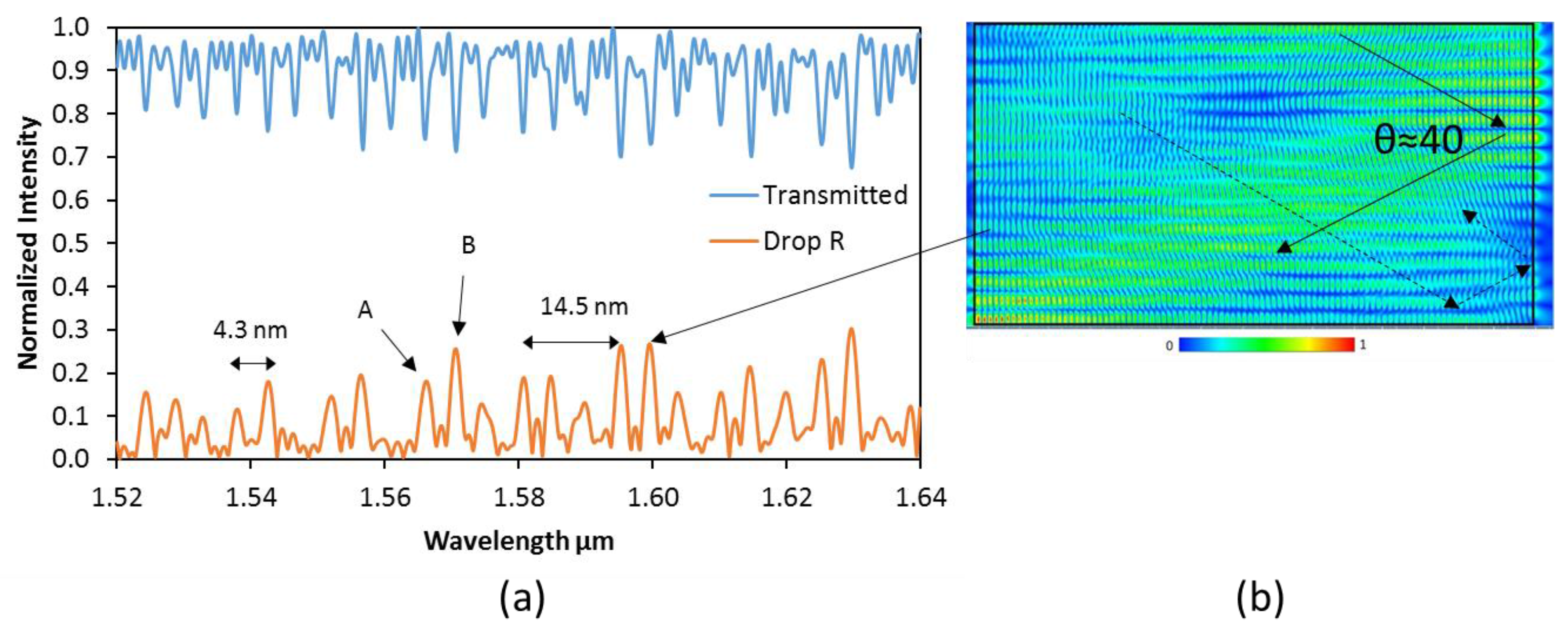
18 time steps; an orthogonal mesh size of 20 nm, and a modulated continuous Gaussian pulse was used as the source. The normalized optical spectra to the input field of the transmitted port and drop R port are displayed in
Figure 2.
From the simulation result, we can observe that there are two main resonances (noted as A and B) that will preferably couple to the waveguide mode with a separation of 4.3 nm and a
FSR of 14.5 nm which is consistent for silicon (refractive index 3.47) at
λ = 1559 for a
θ of 40°. This angle is close to the propagating angle in the bus waveguide calculated with a mode solver to be 47°. It is important to note that the preferred coupling heavily depends on the structure of the bus waveguide as the structure sets the
kwg which in turns selects the matching angle in the
k-vector of the resonator. In other words, the phase of the mode in the cavity needs to match the one in the waveguide, and only the modes that match, will strongly couple. In our case, we fixed the waveguide dimensions to a single mode to avoid losses from coupling to higher-order modes. The spectral response is irregular due to the multimode nature of the cavity as can be seen in-between these two main resonances, where there are low-quality factor modes and their power is much less than the two dominant modes as also found in [
29]. For large square resonators, the shape of the electro-magnetic pattern inside the cavity at resonances seems very similar and some have
mx = 64 and
mz = 16, as displayed on
Figure 2b for the resonance of
λ = 1599.6 μm. This pattern pulsates with time, creating a standing-wave resonator, and thus, it couples the same amount of power to the Drop R and Drop L ports. In
Figure 2b, we can intuitively see this effect with the dashed and solid lines that couple to the opposite direction in the drop waveguide. Furthermore, as the bounces have similar angles in all walls to meet the resonance condition, it is foreseeable that the same results will be obtained regardless of which wall the drop waveguide couples to in a rectangular resonator. Departing from this design, and referencing Equation (2), we first optimized the
Q value by tuning the coupling length and gap size (coupling coefficient
κ), and then accounted for the effect of different rectangular sizes (the
FSR in Equation (2)). We also investigated the performance of the same devices under TM-mode propagation, and demonstrate the symmetry of the device via an eight-port configuration. The results are presented in that order in
Section 4.
3. Fabrication and Experimental Setup
The devices were fabricated on SOI wafers with a top silicon height of 250 nm and a buried SiO
2 box of 3 μm. A spin coater was used to apply the positive resist ZEP520A from ZEON chemicals to a chip. The devices were then patterned directly in the resist using EBL at 75 kV accelerating voltage. Immediately after, the resist was developed with ZED-N50 for 60 s. Then, the device was etched in a single step by ICP-RIE using SF
6 gas at low pressures and an etching time of 2 min to achieve smooth sidewalls. Finally, the resist was removed with the organic dissolver ZDMAC. The fabricated waveguides were 450-nm wide and no upper cladding was added. To access the device, we used fully-etched grating couplers fabricated in the same single etch step as the device. Two sets of devices are fabricated—one with grating couplers designed for TE polarization at the end of the waveguides, and another set with grating couplers for TM polarization. Both grating couplers consist of a matrix of rectangular holes with periods of Λ
x = 700 nm and Λ
Y = 600 nm for TE-polarization [
31], and Λ
x = 940 nm and Λ
Y = 650 nm for the TM mode followed by a linear taper. Both diffraction gratings were designed to have their Bragg wavelength at 1580 nm.
Figure 3a shows the flow diagram of the fabrication process,
Figure 3b displays a scanning electron microscopy (SEM) image of the fabricated device of 20 × 10 μm
2 with a gap of 160 nm and
Figure 3c displays the TM grating coupler.
The experimental setup consists of a tunable laser in the C and L bands (1520 to 1640 nm) connected to a polarization controller using a single-mode fiber. The input and output fibers are placed above their corresponding grating couplers and are tilted 10° with a six-axis stage controller to avoid second-order reflections and to obtain the best coupling power. The output optical power was detected with a photodetector and the chip was thermally stabilized to 25 °C.
4. Results and Discussion
The optical spectra of the transmitted and drop R port of the 20 × 10 μm
2 rectangle, with a gap of 160 nm, are presented in
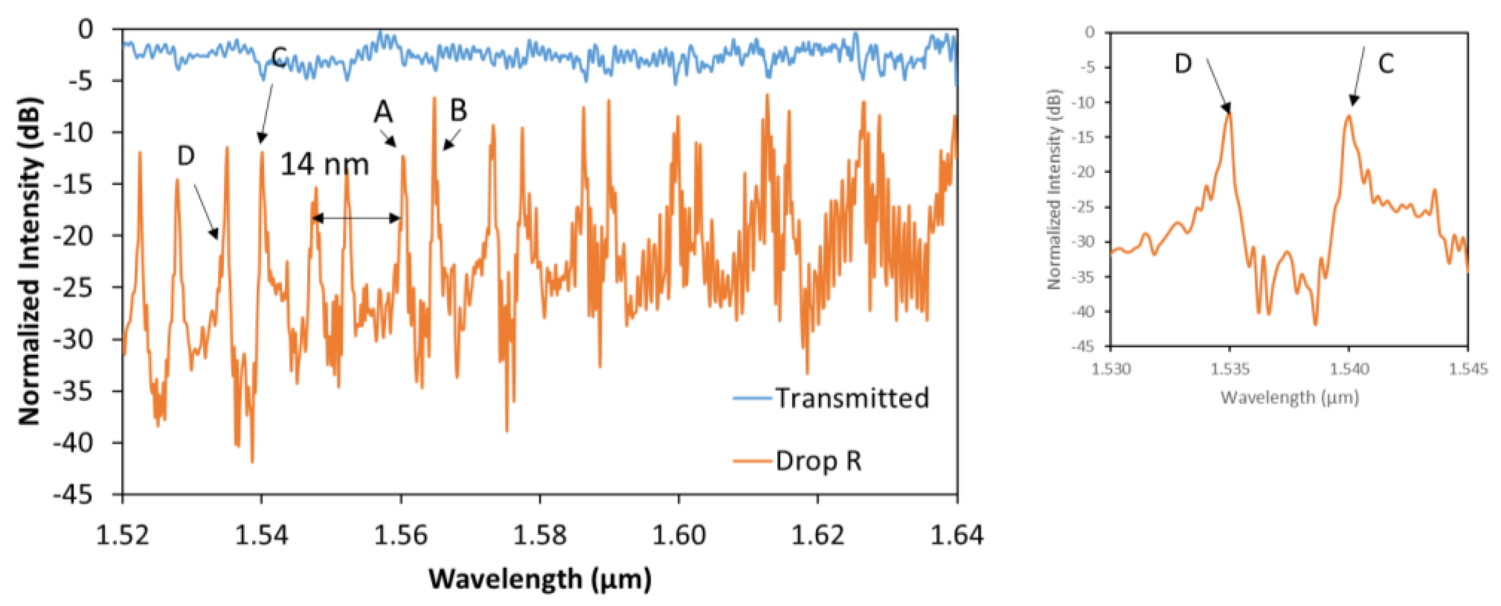
Figure 4 for the TE mode. The powers shown in the following graphs have been normalized using a reference straight waveguide fabricated next to the device. From the experimental results, we can observe the two main resonances (A and B) in the transmission and drop R port spaced 4.4 nm apart with an
FSR of 13 nm consistent with our simulations and a theoretical bounce of
θ ≈ 42° with a
Q value of 4100. A behavior not observed in the simulation is that resonance A approaches resonance B and eventually they resonate at the same wavelength, becoming indistinguishable, because of the group dispersion inside the cavity, which is not considered in the simulations; nevertheless, the simulation is in good agreement with the experimental results. The low-quality resonances cannot be spectrally resolved with our system and those that are close to a main resonance, couple to it, broadening the linewidth of the main one, making most of the resonant peaks asymmetric with fine features as can be seen in the inset of
Figure 4 for resonance C. Also, the reason that, at longer wavelengths, there are more fluctuations is that those wavelengths are in the cutoff frequency of the grating coupler.
From the transmitted port, we can calculate a maximum coupling efficiency of about 50% yielding an extinction ratio of only 3 dB. This is because of the contra-directional coupled power induced by the rough sidewalls [
32]. Also, as stated from the figure of merit called coupling ideality [
33,
34], we can achieve overcoupling, and critical coupling in the system having an impact on the linewidth-power of the peaks. For the modes to overcouple, we need narrow gaps and long interaction areas. Since the minimum achievable gap size is 160 nm limited by our fabrication technology we can only increase the gap to achieve critical coupling. Similarly, the coupling length can only be reduced to account for those coupling regimes. The following sections focus on this figure on merit by modifying the coupling length and gap for three different sizes of resonator operated in TE and TM polarization.
4.1. Coupling Length
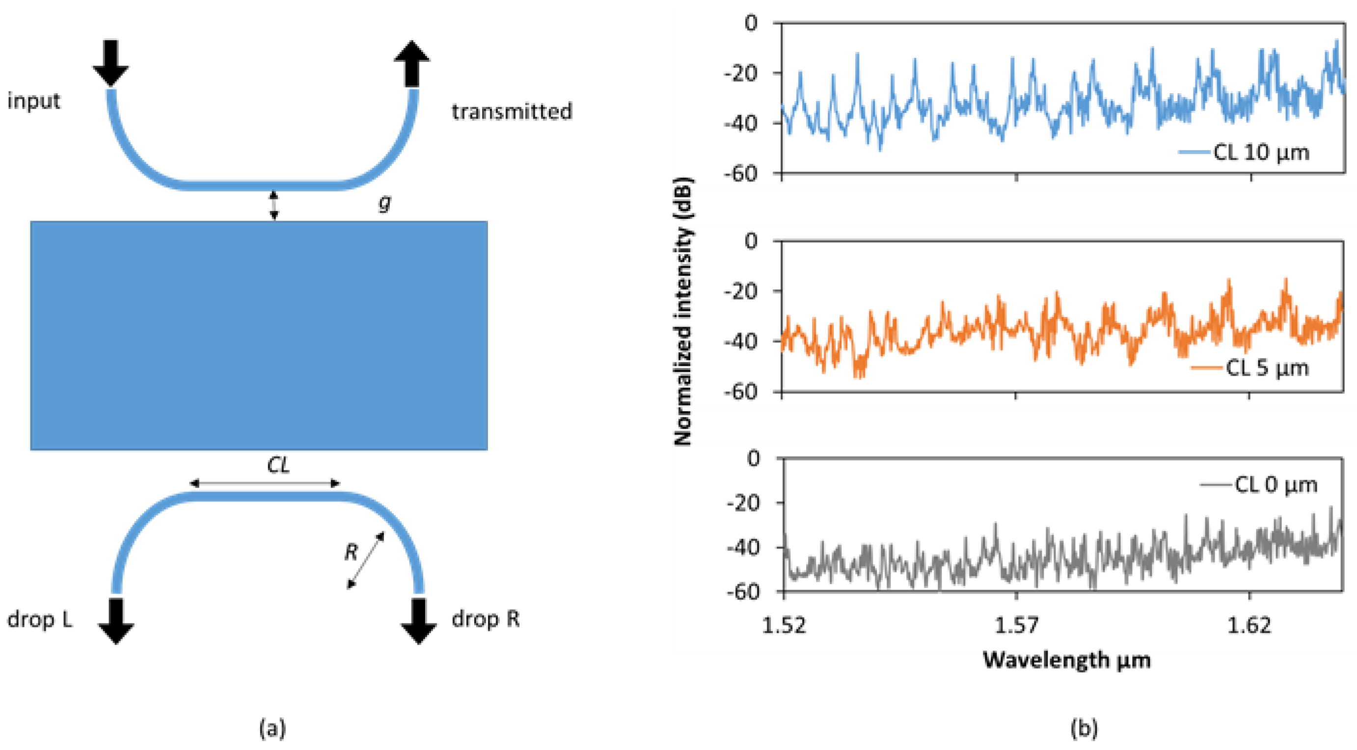
A parameter that influences the coupling coefficient is the coupling length of the device. In the case of rectangular microresonators, the maximum coupling length is given by the length of the rectangle, thus, we can only decrease the length of the coupler. To achieve this, the straight section of the waveguide was shortened, and then immediately after, it was bent outwards with a radius
R = 5 μm to neglect extra losses from the bending, as illustrated in
Figure 5a. We characterized the cases when the straight section was 20, 10, 5, and 0 μm in length, all with a gap size of 160 nm. The dropped spectrum is displayed in
Figure 5b, where we can note that the coupling length reduces the coupled power and it is difficult to resolve for the resonant modes below 5-μm coupling length. We can see that the best
Q factor is for the 10-μm long case, at around
Q ≈ 10,000, an increase from the 20-μm long case. Next, by changing the gap size, we would like to achieve two different things. First, optimize the coupling coefficient, and second, select only one from the two preferentially coupled resonant modes.
4.2. Gap Size
By adjusting the gap size between the bus waveguides and the microresonator, we seek to obtain a similar case to critical coupling as in ring resonators, and thus, increase the
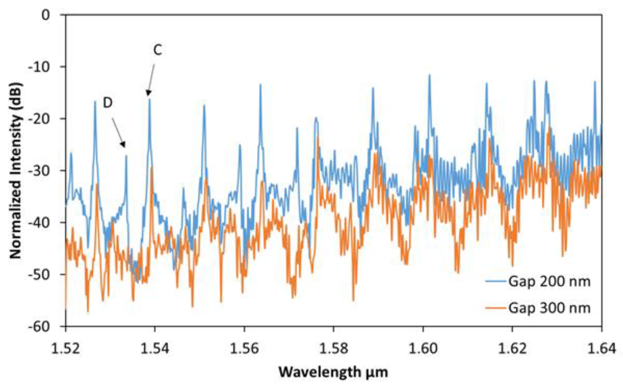
Q factor. The results for different gap sizes are presented in
Figure 6. As the gap increases from 160 to 200 nm, the
Q factor also increases to 12,000, as indicated by resonance (C). For the case when the gap is 300 nm, the dropped power is further reduced, but still have enough power to determine that the
Q factor increases to 13,000 and some resonances are not detected anymore as is the case for resonance (D) from the drop R spectrum. So, by adjusting the gap size to 300 nm, we can select to strongly couple only to one set of WGM (resonance C) with a very high
Q value. The maximum gap size is limited by the noise level of the system as less power is coupled to the cavity. Our highest
Q value for a footprint of 20 × 10 μm
2 is still a bit lower than a ring resonator of a similar footprint and
Q value of 20,000 [
35], with the advantage being that the optical mode is completely distributed inside the cavity, rather than mostly propagating in a nanowire, which is beneficial in sensing applications, where the propagating area of the mode is important for detecting particles.
4.3. Microresonator Size
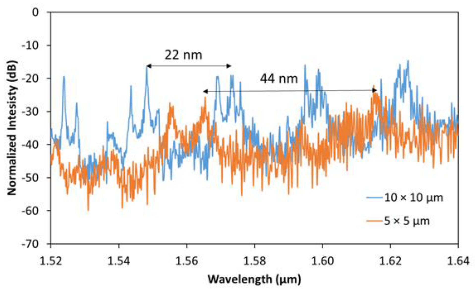
Next, we study the system with different cavity sizes. We performed a similar analysis for different sizes of the square resonators, namely, a 10 × 10 and 5 × 5 μm
2 resonator to reduce the footprint to even less than the required footprint of a ring resonator. The most immediate result is the change in the
FSR to 22 nm for the 10 × 10 resonator and 44 nm for the 5 × 5 resonator which both belong to a bounce angle of
θ = 50°. Next, the coupling length was changed to 0, 5, and 10 μm for the 10 × 10 μm
2 resonator and to 0 and 5 μm for the 5 × 5 μm
2 resonator. The optimum coupling length in terms of
Q factor was found to be the full length of the square, yielding a
Q of 4200 and 1000, respectively. From this trend, we can confirm that the
Q factor is inversely proportional to the size of the resonator as expected by Equation (2) and also as the
Q factor is proportional to the lifetime of the photon inside the cavity, which is longer in bigger cavities. Then we found that the gap size has a similar behavior as in the rectangle case, and the best condition for both cases is when the gap is 160 nm, observing the multimode resonant spectra in the drop port R and enough power to resolve the resonances. The experimental results are presented in
Figure 7 with the optimized parameters for both squares with a 160-nm gap.
4.4. TM Polarization
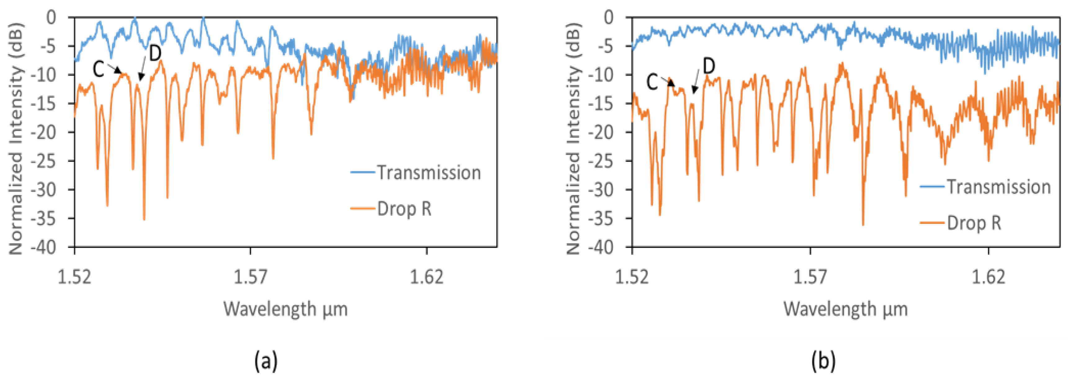
Next, we analyze the system when the polarization is TM as this mode is not affected by sidewall roughness as much as the TE mode. We evaluated the same devices for TM-polarized light and we found similar results as to the case of TE mode in terms of the
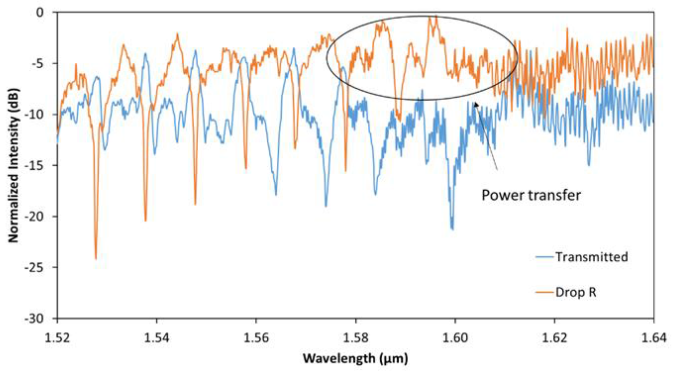
FSR. One difference is that the optical power in the transmitted port decreases significantly at resonant wavelengths, becoming easily distinguishable with high extinction ratios of up to 15 dB. An important case occurs for the 20 × 10 μm
2 resonator with a 160-nm gap as we obtain the highest power transfer of 95% from the transmission to the drop port, as shown in
Figure 8, from 1570 to 1600 nm.
With similar conditions, the coupling efficiency is higher for the TM polarization due to the evanescent profile of the mode as it renders it less susceptible to sidewall roughness and also the waveguide mode phase matches better to the resonant cavity’s mode for the particular waveguide structure. TM modes have longer penetration depth of the evanescent wave resulting in WGMs with broader linewidths and lower
Q values, which is consistent with other published work [
23,
36]. It is important to note that, for the case of TM, we are in the over-coupling regime, so in general, linewidths are broader, and lower
Q values are attained. The two preferably coupled modes cannot be spectrally resolved, due to the broadening of the linewidth and the decrease of the
Q factor. A better spectral resolution was obtained when the gap size was increased and the transmission and drop R spectra are shown for a gap of 200 nm,
Figure 9a, and 300 nm,
Figure 9b. For the 300-nm gap case, we can detect both modes, but the
Q value still remains below their respective version of TE as the bus waveguide mode is constant.
Again, the previous results for the TE mode hold true in terms of the effects in the
Q factor of the gap size, coupling length and coupled power but their optimum values change by a significant amount and are summarized in
Table 1 for both polarizations.
4.5. Eight-Port Devices
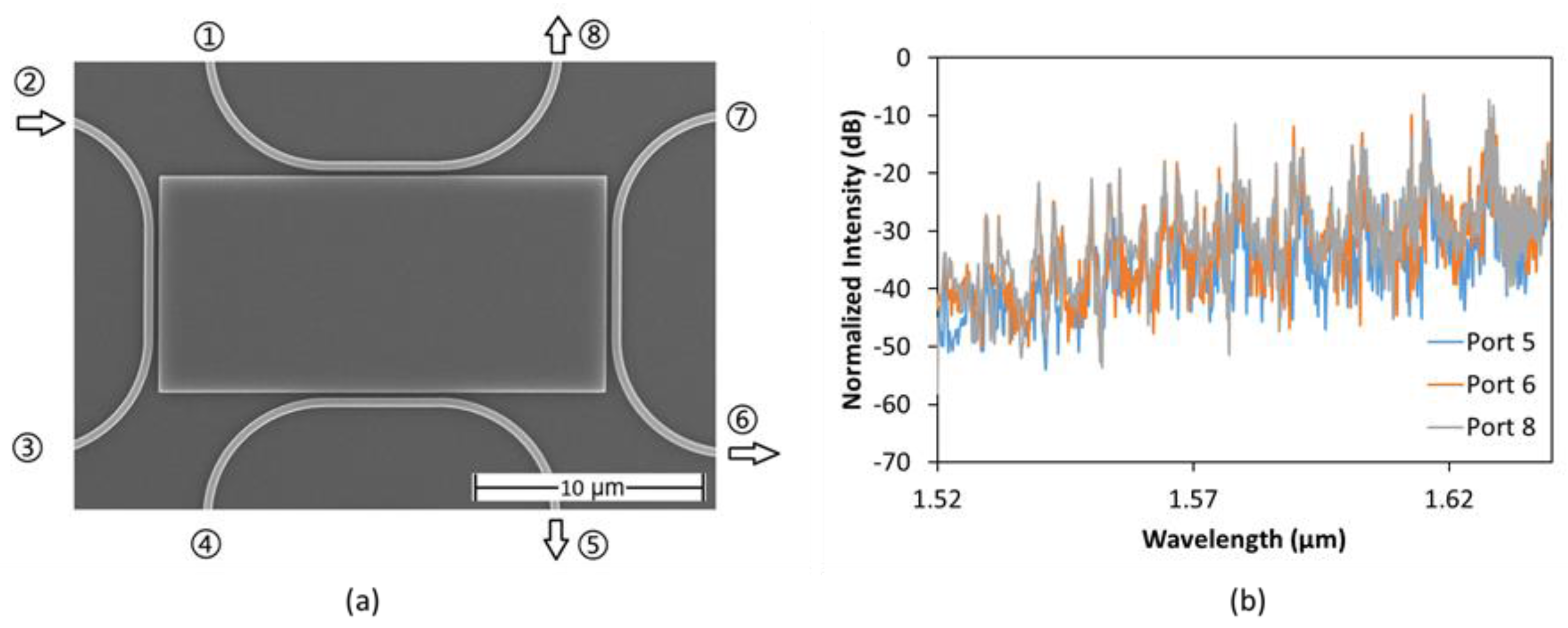
Finally, we propose an eight-port device to investigate the symmetry of the system. We added two extra waveguides evanescently coupled to the lateral sides of the 20 × 10 μm
2 rectangle and detected the power coupled to all ports of the resonator. Taking into consideration that the best design for the 20 × 10 resonator is the one with a 160-nm gap, we fabricated a device with that characteristics for all waveguides. Considering all waveguides have the same coupling length, we chose 10 μm since it is the longest possible size for all waveguides. The SEM image of the proposed device is displayed in
Figure 10a as well as the optical power in
Figure 10b from ports 5, 6, and 8 when port 2 is excited by the TE mode. We found that the system is completely symmetrical in all ports, confirming that the standing wave inside the resonator couples outwards to all the drop waveguides. At resonance, the standing wave inside the resonator suggests that the evanescent field from all sides of the rectangle is identical. Analyzing the system with ray optics, we have a symmetrical response on all waveguides because the bounce angles on all the sidewalls are very similar, and since all waveguides are identical, they preferentially couple to the same resonant mode. This kind of configuration has applications in power splitting, signal routing, and 90° bends.
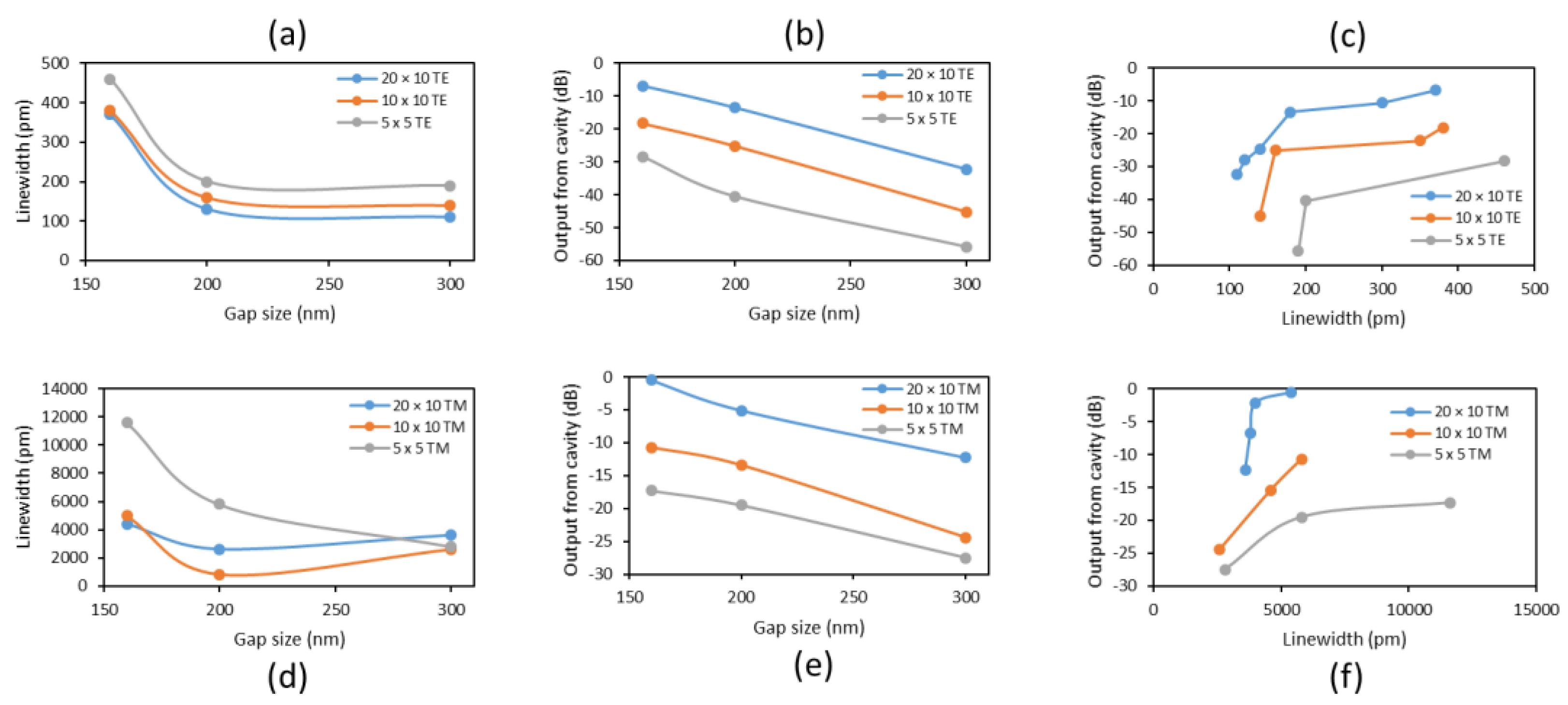
In order to summarize the results, it is possible to use the figure of merit called coupling ideality, so that the dropped power and linewidth of the resonances are given as a function of gap size. The results are shown in
Figure 11. It is important to note that for TM mode, it is difficult to calculate the bandwidth of some resonances, as many resonances overlap with each other.
From
Figure 11a, we can see that as the gap size increases for the TE mode, the linewidth decreases exponentially, and below a certain point, the output power from the cavity is too low to distinguish the resonance from the noise level as shown in
Figure 11b because the output power also decreases logarithmically with increasing gap sizes. In terms of cavity size, the bigger the cavity, the lower the linewidth and the higher output power for the same gap size. Longer interactions between bus and cavity allow for more power to be coupled. From
Figure 11c, we can see that as the linewidth is reduced, so is the output power from the cavity, up to a point where there is no more detectable power coming out of the cavity. Before this point, the minimum linewidth is achieved, and depending on the required threshold power of the application, the linewidth is limited. For TM mode, the results are a bit different since the gap size and linewidth do not follow a constant decay, but rather there seems to be an optimum point for the smallest linewidth in the resonator for large cavities as shown in
Figure 11d. As a similar trend, the larger the gap, the less the power is coupled to the resonator as shown in
Figure 11e. Finally, in
Figure 11f, we can confirm a similar behavior than the TE case, but the output power is much higher being able to achieve critical-coupling. In general, there is more output power with TM mode than TE mode, and the linewidths are narrower for TE as found in the previous section. These results are completely symmetrical, regardless of the side of the resonator we couple to and from.

