Article

High-Resolution Arrayed-Waveguide-Gratings in Astronomy: Design and Fabrication Challenges

innoFSPEC, Leibniz-Institut für Astrophysik (AIP), 14482 Potsdam, Germany
*
Author to whom correspondence should be addressed.
Photonics 2017, 4(2), 30; https://doi.org/10.3390/photonics4020030
Submission received: 3 March 2017 / Revised: 4 April 2017 / Accepted: 5 April 2017 / Published: 10 April 2017

Abstract

:
A comprehensive design of a folded-architecture arrayed-waveguide-grating (AWG)-device, targeted at applications as integrated photonic spectrographs (IPS) in near-infrared astronomy, is presented. The AWG structure is designed for the astronomical H-band (1500 nm–1800 nm) with a theoretical maximum resolving power R = 60,000 at 1630 nm. The geometry of the device is optimized for a compact structure with a footprint of 5.5 cm × 3.93 cm on SiO2 platform. To evaluate the fabrication challenges of such high-resolution AWGs, effects of random perturbations of the effective refractive index (RI) distribution in the free propagation region (FPR), as well as small variations of the array waveguide optical lengths are numerically investigated. The results of the investigation show a dramatic degradation of the point spread function (PSF) for a random effective RI distribution with variance values above 10 4 for both the FPR and the waveguide array. Based on the results, requirements on the fabrication technology for high-resolution AWG-based spectrographs are given in the end.

1. Introduction

Arrayed-waveguide-grating (AWG) devices have been established as the most common wavelength division multiplexers (WDMs) in optical telecommunications [1,2,3]. The potential of AWG technology motivated the research of applications in spectroscopy and sensing, such as biomedical Raman spectroscopy [4], interrogation of fibre Bragg grating sensors [5] and micro-ring resonator sensors [6]. In the field of astrophotonics, the AWG technology received attention as a possible candidate for the realization of astronomical integrated photonic spectrographs (IPS) [7,8]. The planar nature and compactness of the AWG devices provide a much greater robustness against misalignment due to flexure and thermal drift than conventional bulk optics, as well as easy shielding against external influences. The compact size and light-weight feature of an IPS may prove favourable for airborne and spaceborne astronomical instrumentation. A further advantage is the possibility to combine the IPS with additional integrated photonic elements on a single compact chip (‘lab-on-a-chip’ concept), such as micro-ring resonators for wavelength calibration or sensors for chemical and biomedical analysis. Although IPS devices have been shown to be no viable alternative to large conventional integral field spectrographs for extremely large telescopes, they can be useful in combination with small, diffraction-limited telescopes [9]. Potential applications of an IPS include diffraction-limited single-object spectroscopy and low-resolution multiplexed spectroscopy. The feasibility of IPS application in astronomy has been previously demonstrated using a commercial silica-on-silicon (SoS) AWG device, with a reported resolving power R ∼ 2500 at 1600 nm [10,11]. However, commercial AWG devices are specifically designed and optimized for optical channel (de-)multiplexing in telecommunications. As such, they are not well suited for many scientific applications in astronomy, spectroscopy and sensing. For example, radial velocity measurements of stellar objects require a much higher resolution. The migration of AWG technology from telecommunications to astronomical applications must go through new designs with custom-tailored properties. Extraordinarily high requirements on AWG device performance for spectroscopy and sensing create challenges in the design and fabrication previously not encountered in traditional telecom applications. This paper explores some of the most important challenges, in particular the influence of random effective RI variations across the wafer on the performance of large, high-resolution AWGs.

2. Principle of the AWG-Based IPS

The AWG is a planar integrated waveguide structure consisting of two slab waveguides called free propagation regions (FPRs), which confine the optical field perpendicular to the plane of propagation, but allow free propagation in the lateral directions. Both FPRs are connected to an array of single-moded waveguides of specific optical length, as shown in Figure 1. On the input side, light is injected into the first FPR via input access waveguides, the diverging beam excites the waveguide array, which guides the light to the second FPR, where beams emitted from each array waveguide interfere constructively, forming a diffraction image on the output facet. The fixed path length difference between adjacent waveguides causes a wavelength-dependent tilt of the output wavefronts, producing a spectrally dispersed diffraction image which can be coupled into output access waveguides (e.g., for wavelength division multiplexing in optical communication), or sampled directly using an image sensor for applications in spectroscopy.
The most prominent difference in device layout between a WDM-AWG and an IPS-AWG is the absence of access waveguides at the output FPR facet of the device. Fixed output access waveguides on a conventional AWG can be thought of as discrete sampling points where the intensity of the focused diffraction image is measured, though the spatial resolution of the spectrum that is sampled in such a manner is relatively low due to the large distance between output access waveguides. In order to utilize an AWG device for the acquisition of spectra, it is necessary to sample the diffraction image at the output FPR facet with a high spatial resolution. The imaging of the focused PSF requires direct access to the output facet of the FPR, for which reason the access waveguides of the output FPR can be cut away from the AWG chip.
The re-imaging of the output spectrum of the AWG currently requires external bulk optics to cross-disperse and separate the overlapping spectra of different spectral orders [10], since the free spectral range (FSR) of an AWG is limited to a few tens of nanometers. Such a configuration is called semi-photonic IPS, since the system is only partially integrated into the photonic chip [9]. The curvature of the image plane (Rowland circle) causes defocus aberration for off-axis beams, which decreases the resolving power at off-axis wavelengths. Several methods of defocus correction are available, such as field flattening by integration of a lens into the FPR [12], non-Rowland configurations utilizing a three-stigmatic-point method [13], and re-imaging of the spectrum using defocus-compensating bulk optics [11].
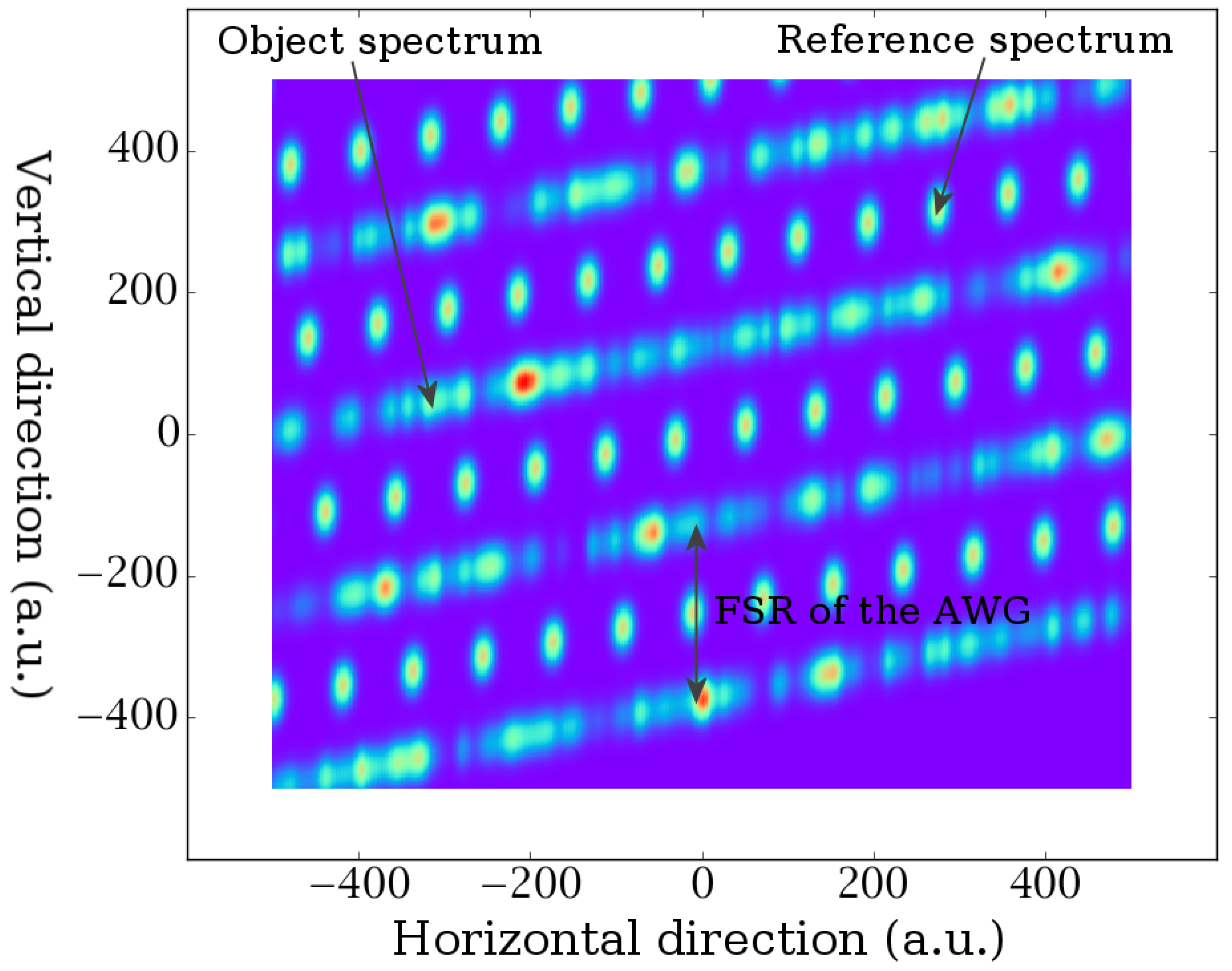
A schematic example of an IPS system utilizing cross dispersion is shown in Figure 1. In this schematic, a single-input AWG chip is connected to a light source (e.g., from a telescope) and a calibration source which generates a known reference spectrum, such as a gas reference cell or a frequency comb generator, via single mode fibres (SMFs). Figure 2 illustrates the two-dimensional structure of the cross-dispersed spectrum on the image sensor. An alternative configuration to the cross-dispersive system is a stack of multiple identical AWG chips, which can increase the total wavelength range of the spectrograph and enable multi-object spectroscopy.

3. Features of the AWG Design

3.1. Target Application and Material Platform

The primary application for this particular AWG design is the study of M-class dwarf stars with surface temperatures in the range 2300–3800 K [14], which emit roughly two thirds of their total EM power output in the NIR wavelength region according to Planck’s law. Considering observations with ground based telescopes, the astronomical H-band is chosen as the wavelength range of the AWG. This choice is backed by the requirement of compatibility with single-mode fibres of the type SMF-28, which operate in single-mode regime above 1260 nm and exhibit minimum loss at 1550 nm [15]. Other criteria for the material platform include high compactness of the planar structure, low waveguide propagation losses, low dispersion and broad wavelength range for linear, transparent light propagation. Generally, it is difficult to find a specific platform that satisfies all of these criteria. For example, high RI contrast silicon-on-insulator (SoI) technology offers a very high compactness of the waveguide structure with the additional advantage of possible integration of opto-electronic elements on the same platform, but may prove difficult to achieve ultra-low propagation losses and high coupling efficiency with SMFs. In the case of a silicon-based AWG, the imaging of the dispersed spectrum by means of external bulk optics can also be problematic, if the focused spot diameter of the image is below the diffraction limit in air. Similar problems may arise with other high-RI-contrast material platforms, such as Si3N4 on SiO2. Although low-loss, fibre compatible high-index waveguide structures have been demonstrated [16,17], their fabrication involves additional steps and requires modifications of the traditional lithographic processes. In order to avoid complications, Silica-on-Silicon (SoS) material platform with a refractive index contrast of 1.5% was chosen for the AWG design due to good fibre compatibility, low absorption in the NIR wavelength range and low propagation losses of 0.01 dB / cm [18], amongst other advantages.

3.2. General Structure of the AWG

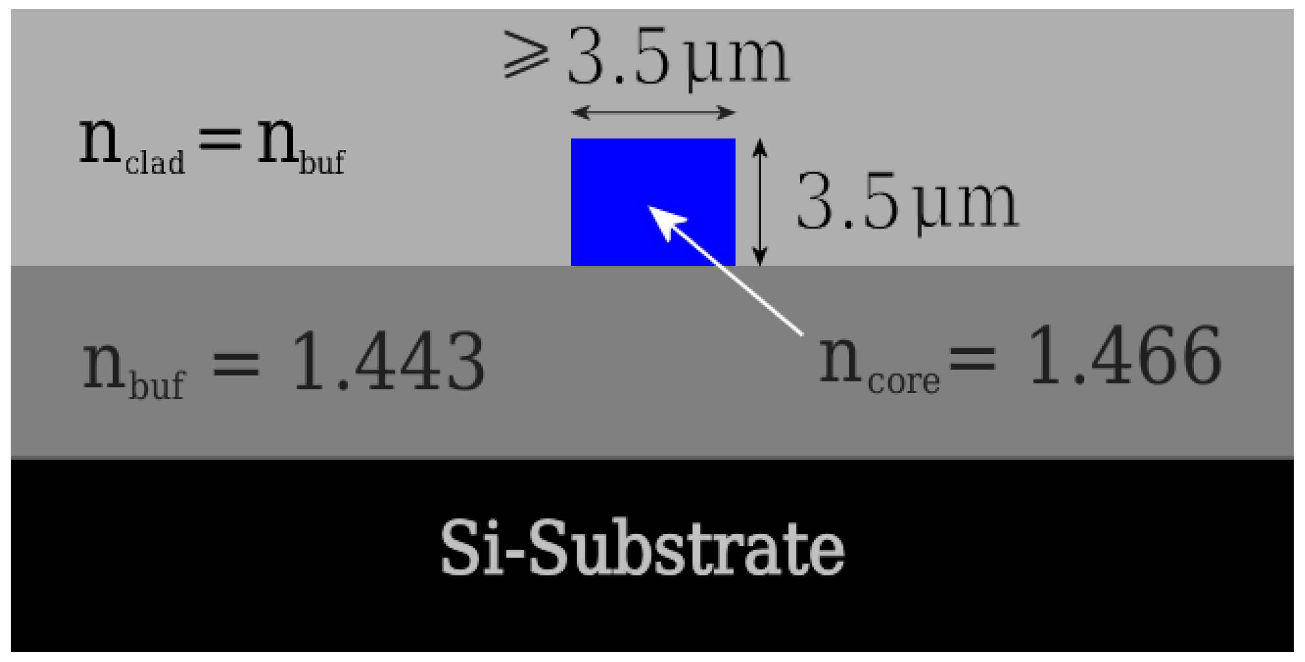
The AWG device features an array of 800 single-mode, rectangular buried channel waveguides (Figure 3) with core dimensions 3.5 μm × 3.5 μm. The AWG is arranged in a folded configuration (see [19]). The refractive index of the SiO2 buffer and cladding is 1.443 and the core refractive index is 1.466 ( Δ = 0.015 ) at the central wavelength of 1630 nm. The mode field diameter equals 4.7 μ m. Circular waveguide bends with a fixed radius of 3000 μ m, which is the minimal radius at the longest expected wavelength of 1800 nm, are used to minimize systematic phase errors. The physical path length difference between adjacent waveguides is 111.2 μ m, which corresponds to a grating order of 99 and an FSR of 16.15 nm.
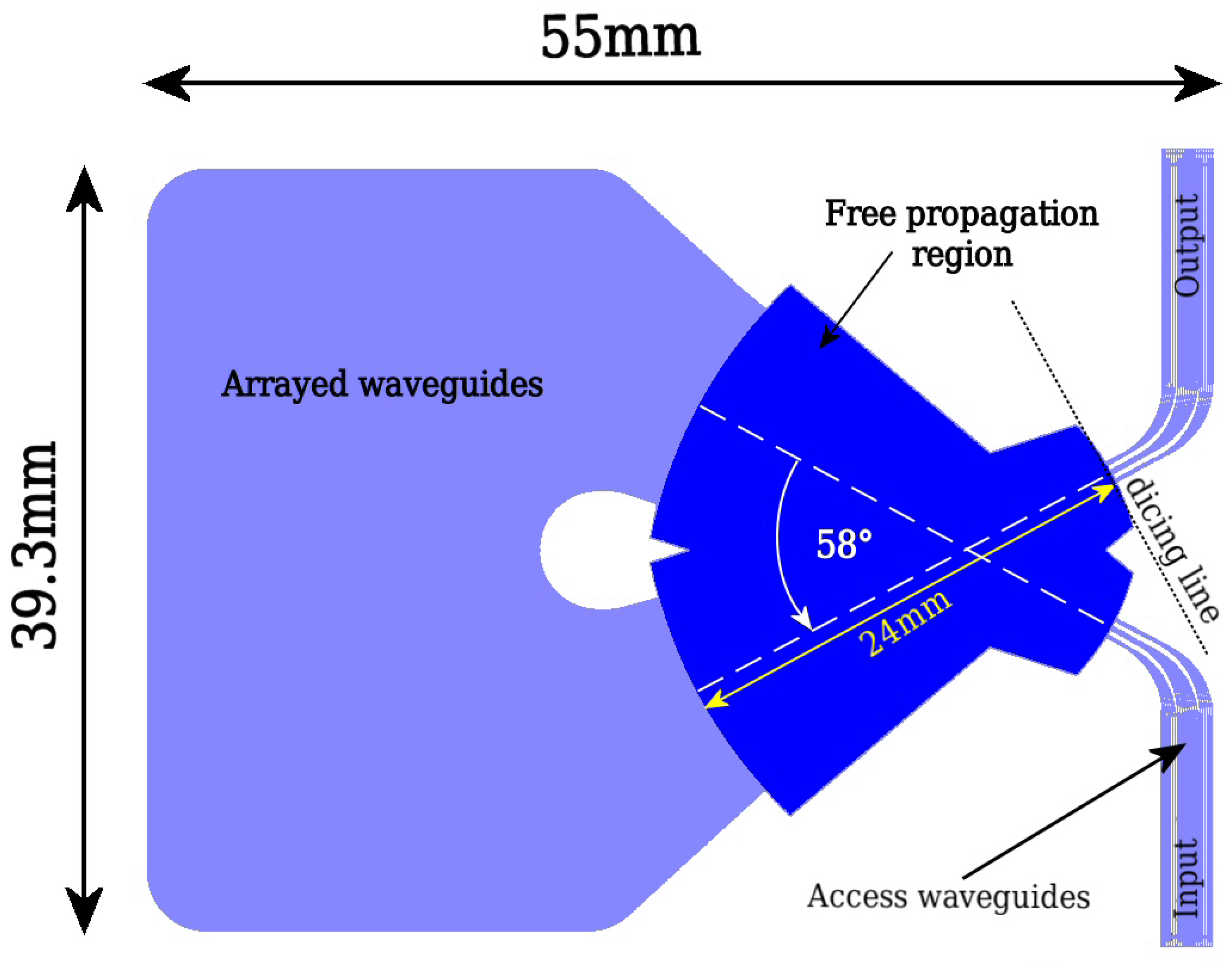
The waveguide array is connected to a single FPR consisting of two identical overlapping slab waveguides, which is used for both input and output. Connections with external instruments are established through 21 input/output access waveguides arranged in three distinct groups, which are specifically designed for spectrograph operation. A schematic of the AWG design is shown in Figure 4. The output access waveguides are included for characterization purposes. Once the AWG passes the quality test, the output access waveguides can be cut away following the dicing line as shown in Figure 4.

3.3. Customized Input Waveguide Interface

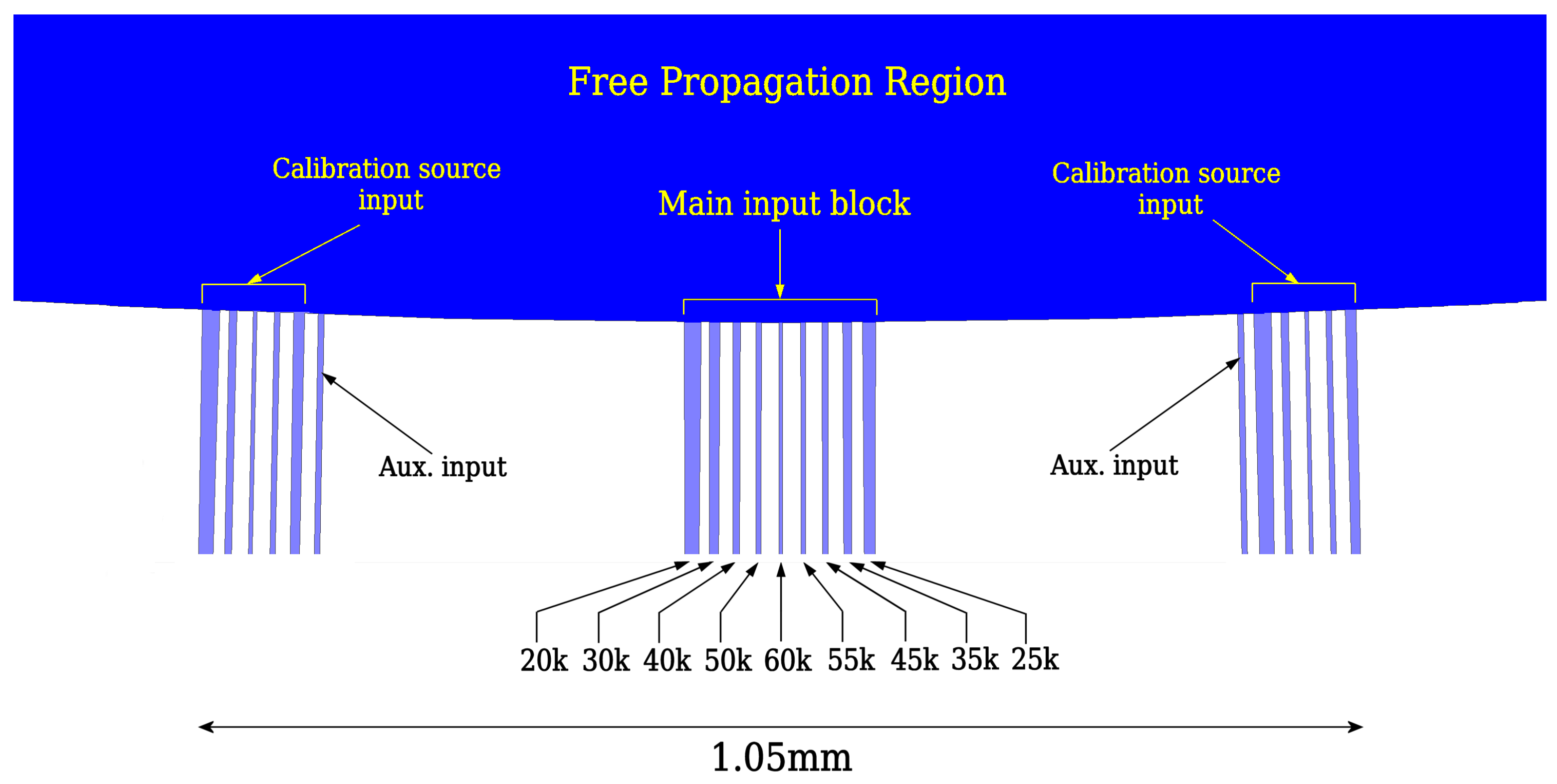
The IPS design features a customized input interface, which is not yet realised in any commercial AWG device. The access waveguide bundle is subdivided into three distinct groups. Nine waveguides at the centre of the interface serve as inputs for the object signal. The spot size at the waveguide-FPR junction is controlled by adjusting the width of the tapering in order to enable operation at different resolving powers (see [20,21]). Input ports with the highest resolving power are located close to the central axis of the FPR in order to minimize the off-axis degradation of the beam, while inputs with lower resolving powers reside on the periphery of the central waveguide group.
The peripherial groups of waveguides are designated input ports for an external calibration spectrum source. The location of these input waveguide groups is chosen specifically to be ±1/4 of the total aperture width in order to separate the object spectrum from the calibration spectrum in the cross-dispersed image. A schematic of the input interface is shown in Figure 5. Tapering widths and corresponding resolving powers are listed in Table 1.

3.4. Loss Reduction by Modification of the FPR-Array Interface

The width of the arrayed taper waveguides at the FPR-array junction should match the grating pitch of the AWG as closely as possible in order to minimize scattering losses during the transition from the FPR to the waveguide array. On the other hand, the waveguide integration density is limited by evanescent field interaction of adjacent waveguide cores, especially at longer wavelengths and long propagation lengths in case of a large scale high-resolution AWG. It is therefore necessary to observe a sufficient minimum distance between adjacent array waveguides. An optimum grating pitch of 14 μ m was found for the high-resolution AWG through BPM simulations of evanescent field cross-coupling in the fan-out regions of the waveguide array. However, taper waveguides of this width support several propagating modes, which leads to losses due to higher order mode excitation at the FPR-array transition. Numerical 3D-BPM simulations of the transition region with continuous, linear tapering show a coupling loss of 6.9 % at 1500 nm.
A simple method based on two-mode interference was devised for the high-resolution AWG design in order to reduce the coupling losses in the FPR-array transition region. The continuous, linear taper was replaced with a discontinuous piecewise linear taper which acts as a multimode interference (MMI) coupler and utilizes the interference of the 0th order mode and the 2nd order mode to achieve efficient coupling of both mode components into a single mode waveguide.
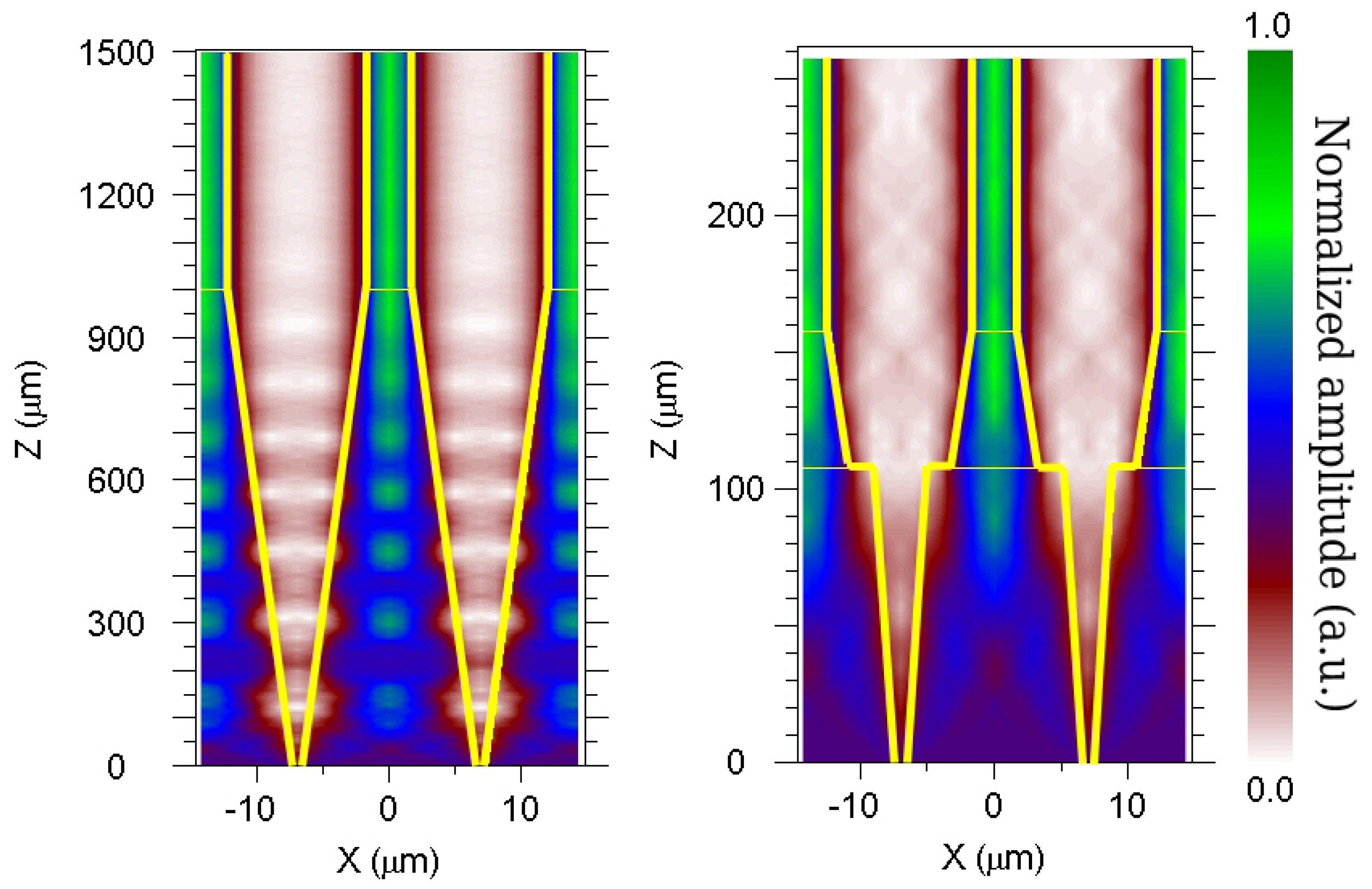
The first segment of the coupler supports four propagating modes. Multimode propagation is terminated at the location of the first constructive interference maximum, where the multimode waveguide connects to a second segment of reduced width, whose fundamental mode matches the field at the end of the multimode segment. Figure 6 shows propagation in a linear taper waveguide (left) and the modified discontinuous MMI taper (right). A strong, decaying beating pattern is observed in the linear taper waveguide, indicating the presence of multiple propagating modes.
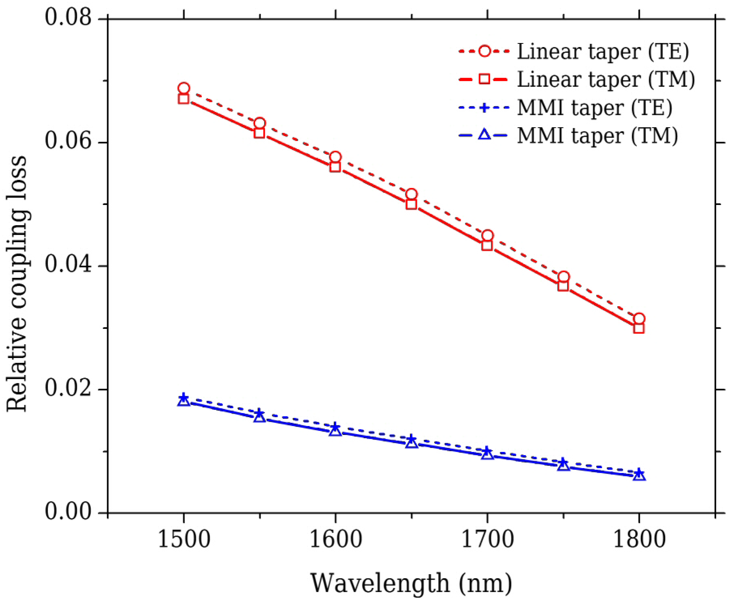
Coupling from the input FPR into the array waveguides was simulated for both types of tapering using 3D-BPM with transparent boundary conditions (TBC) and Crank-Nicholson numerical scheme. Taper performance was studied for both TE and TM polarizations. The simulation results show a reduction of coupling loss from 6.9 % with ordinary linear tapering to less than 2 % with discontinuous tapering at 1500 nm. Losses decrease with increasing wavelength for both types of taper waveguides. However, the discontinuous taper outperforms the ordinary taper in the entire wavelength range 1500 nm–1800 nm by a margin of 2 % 4.9 % . The simulated coupling losses for the linear taper and discontinuous taper in the wavelength range 1500 nm–1800 nm are shown in Figure 7.

4. Fabrication-Tolerance Investigation

The functionality of high-performance planar integrated spectrographs on the basis of AWG and Echelle-technology critically depends on the quality of fabrication and the attainable degree of layer homogeneity, as well as reliable reproducibility of optical waveguide properties. The maximum resolution achievable in practice is limited by random spatial variations of the mode propagation constant in the FPR and, in case of AWGs, random variation of array waveguide optical length. The effects of deviations from the ideal case are studied in this section.

4.1. Effects of Random Perturbations of the Refractive Index Distribution in the FPR

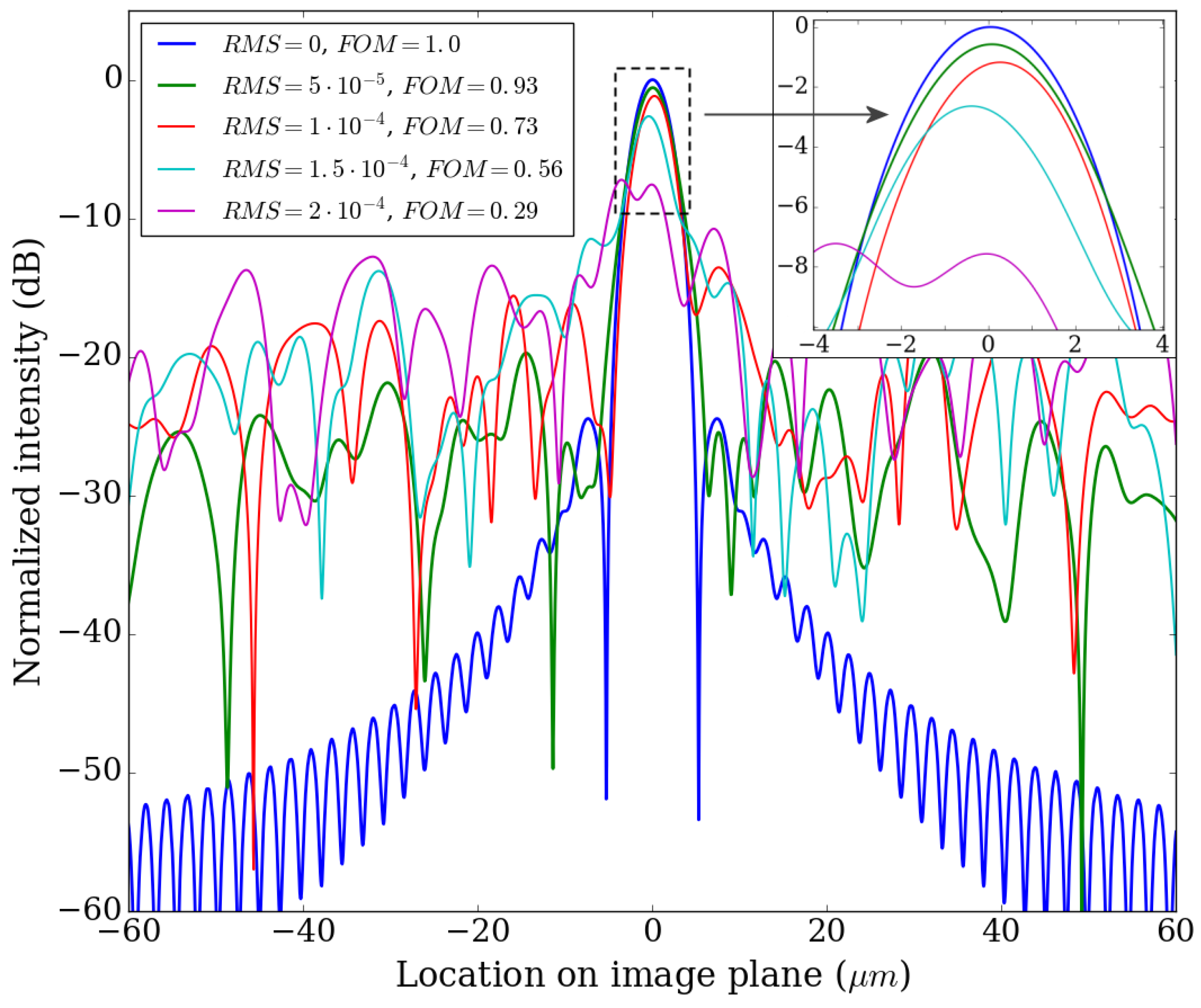
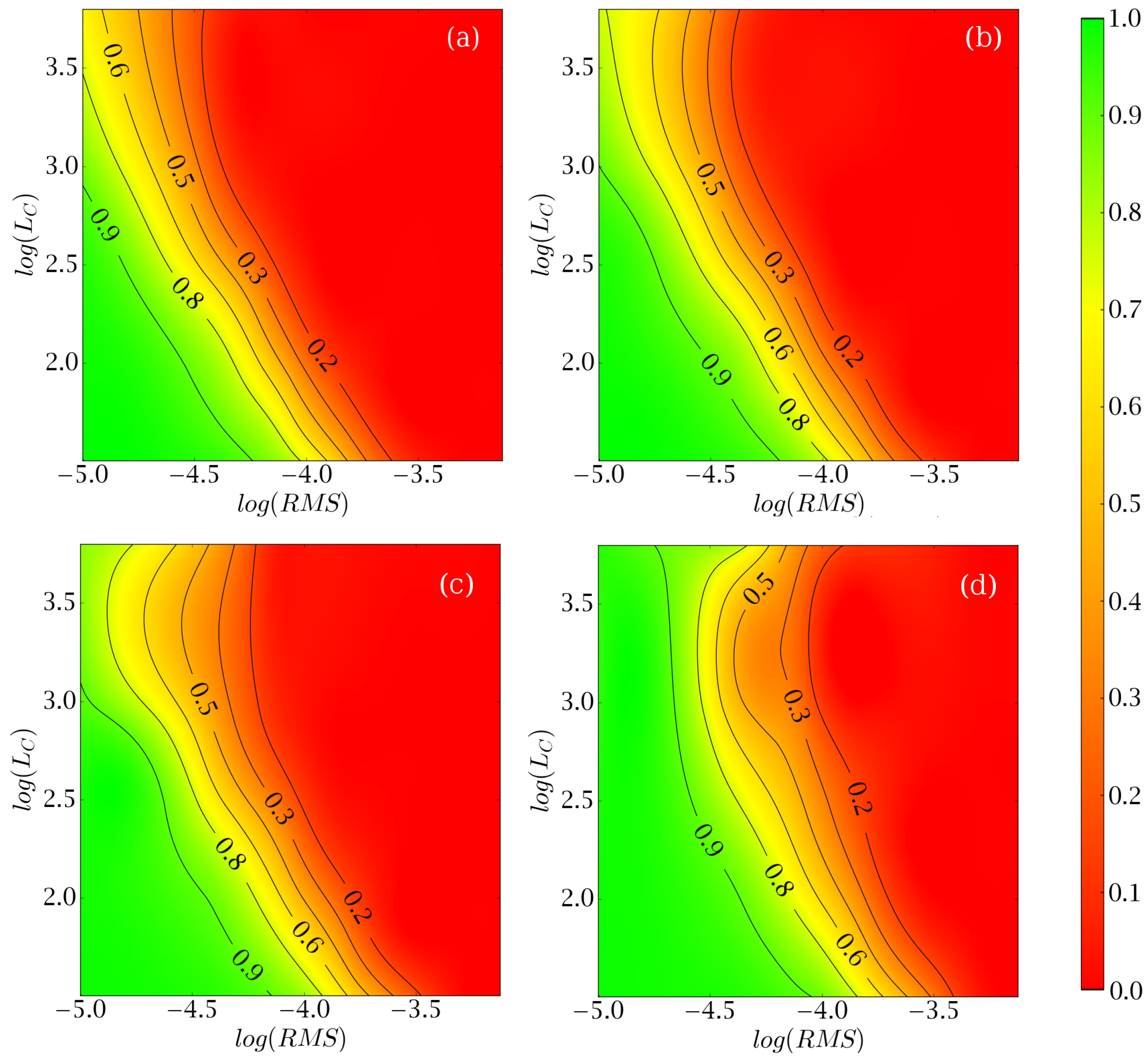
The focusing behaviour of the AWG in the presence of spatial effective index variations in the FPR was studied on a 2D-model of the input and output FPRs using wide-angle BPM at 50 nm lateral resolution and a propagation step size of 500 nm. The FPRs were overlaid with a randomly generated two-dimensional effective RI profile with a Gaussian variation range σ (RMS), spatial coherence length L C and mean slab mode effective index n ¯ e f f = 1.458222 . The effective RI distribution is a combination of material refractive index variations and variations of waveguide geometry. The parameter L C is related to the average distance between two adjacent local maxima of the effective RI distribution and is defined in a similar way as the correlation length of surface roughness profiles [22]. The AWG was simulated for a single wavelength (1600 nm) and the diffraction image after propagation through the non-uniform FPR was compared with the diffraction image in the ideal case. An ideal, unperturbed waveguide array was assumed. The figure of merit (FOM) was obtained through the normalized overlap integral of the image intensities, defined as
F O M = a a f ( x ) g ( x ) d x a a f 2 ( x ) d x a a g 2 ( x ) d x ,
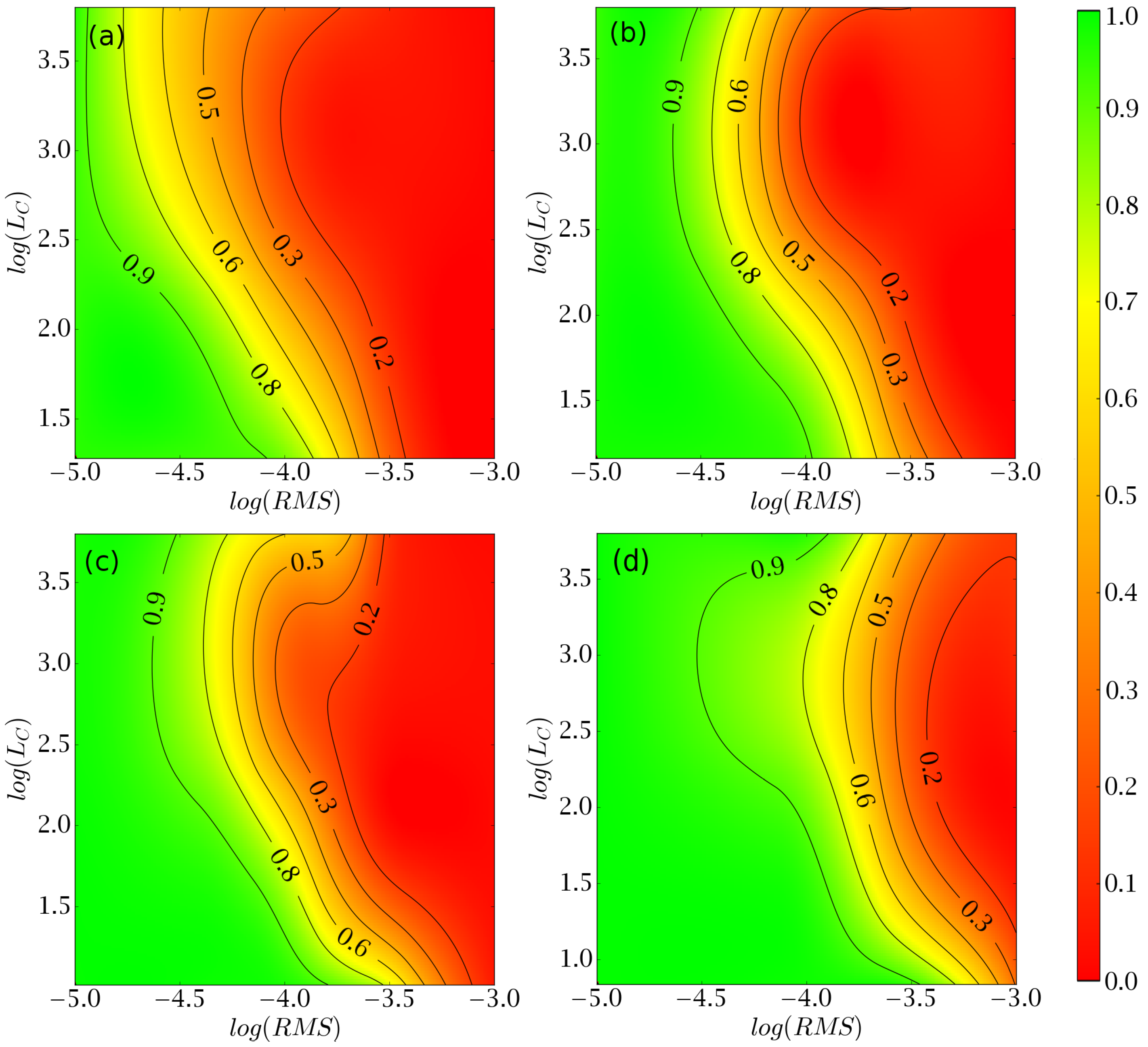
where f ( x ) and g ( x ) are intensities of the diffraction images, x is the location on the image plane and ( a , a ) is the region of interest, which contains the focused PSF. Similar simulations were performed on three smaller versions of the AWG with shorter free propagation lengths of 18 mm, 12 mm and 6 mm in order to study the impact of random distribution of FPR effective index on different length scales. Figure 8 compares simulated PSFs in the presence of FPR refractive index perturbations with the ideal PSF in the unperturbed case for a RMS parameter range 10 5 5 × 10 4 and fixed L C = 63 μ m. Only slight distortion of the PSF is observed at R M S = 10 5 , however, the diffraction image significantly degrades for R M S > 5 × 10 5 . The critical threshold for the FOM value is found to be 0.7 through examination of diffraction images in comparison with the unperturbed case. Figure 9 shows two-dimensional FOM maps for propagation lengths 24 mm (a), 18 mm (b), 12 mm (c) and 6 mm (d). In these maps, the critical FOM value of 0.7 defines a boundary between the region of sufficient RI profile smoothness on the left side (green) and the region of failure on the right side (red). The results of the simulations show that the impact of effective RI variations in the FPR on the IPS performance depends both on the magnitude and the coherence length of the RI variations. The most severe image degradation is observed for coherence lengths on the order of 1mm, as can be seen from Figure 9b–d. Shorter coherence lengths seem to alleviate the PSF degradation and increase the tolerance against larger RMS values for a given AWG resolving power. Critical RMS values are shown to depend on the FPR propagation length as well as the coherence length of effective RI variation. The high-resolution AWG (Figure 9a) exhibits full loss of its focusing ability for RMS values above 10 4 in the entire range of effective RI coherence lengths. The condition is relaxed in smaller AWGs (Figure 9d).

4.2. Effects of Random Effective RI Variations in the Waveguide Array Region

Highly dispersive AWG devices are very susceptible to phase error accumulation over large propagation lengths due to random variations of waveguide core and cladding RI and/or waveguide core thickness and geometry. Since one full spectral order ( λ m i n , λ m a x ) corresponds to a phase difference between adjacent waveguides in the range ( π , π ) , complete loss of AWG functionality is expected for
| δ n e f f | > λ 2 L ,
where δ n e f f is the relative effective index difference between two adjacent array waveguides, λ is the wavelength and L is the physical propagation length. In the case of the high-resolution AWG, the total cumulative path length difference between the first and the last array waveguide is 111.2 μ m × 800 = 88,960 μ m, which corresponds to a hard limit δ n e f f < 9 × 10 6 for the longest array waveguides.
The behaviour of the AWG under spatial RI variations in the waveguide array region was studied, using a similar approach as in the case of the FPR, in order to obtain specific thresholds for the acceptable wafer inhomogeneity under the assumption of unperturbed FPRs. The random variation of optical lengths in the waveguide array was modeled by averaging randomly generated wafer RI profiles along the waveguide paths. The resulting waveguide effective index distributions were used in a numerical model of the AWG to study the degradation of the diffraction image. The FOM for the resulting diffraction images was again obtained using Equation (1). The results of the evaluation are shown in Figure 10.
As in the case of the FPR, the FOM maps show a dependence on RMS and spatial coherence length L C , as well as propagation length. However, the observed influence of the propagation length is significantly weaker for the waveguide array, as the comparison of results for propagation lengths of 10.5 cm (Figure 10a) and 3.8 cm (Figure 10d) shows. Critical RMS values are found to be 10 4 for the largest waveguide array (800 waveguides, 10.5 cm propagation length) and 3.6 × 10 4 for the smallest waveguide array (200 waveguides, 3.8 cm propagation length). The critical thresholds obtained from the simulations are much higher than the estimated limit of δ n e f f < 9 × 10 6 according to Equation (2) due to the averaging of the RI variations over long propagation distances that somewhat evens out the accumulated phase errors.

5. Discussion

A high-resolution AWG design on the SiO2 platform has been introduced in this work. Optimization of the geometrical structure resulted in a footprint of 5.5 cm × 3.93 cm with 800 arrayed waveguides and a focal length of 24 mm. An application-specific input interface with three separate groups of input access waveguides was designed. A modification of the FPR-array transition region was devised in order to reduce coupling losses due to higher order mode excitation in the taper waveguides of the interface by 2 % 4.9 % in the H-band wavelength range (1500 nm–1800 nm).
The impact of random spatial refractive index variations in the FPR and in the waveguide array was studied through numerical simulations of AWGs of different sizes. The FOM values were obtained for RMS values between 10 3 and 10 5 and coherence lengths in the range between ∼6 μ m and 6 × 10 3 μ m. The results of the numerical study show a high sensitivity of the AWG to random spatial refractive index variations both in the free propagation region and in the waveguide array region. In both cases, a dependence of the FOM on the propagation length, the variation RMS and coherence length is observed. For the FPR it is shown that large-scale AWG devices require a fabrication technique which can reliably produce silicon dioxide films with a refractive index non-uniformity R M S < 6.8 × 10 5 in order to meet the criterion F O M > 0.7 for a coherence length L C = 100 μ m. The condition becomes more strict for L C = 1000 μ m, where a non-uniformity R M S < 2.5 × 10 5 is required. A slightly different behaviour is observed for the smallest AWG model with a nonuniformity condition R M S < 1.5 × 10 4 for L C = 100 μ m, R M S < 1.2 × 10 4 for L C = 1000 μ m and R M S < 1.58 × 10 4 for L C = 3000 μ m. The slight relaxation of the FOM condition for longer coherence lengths in the small AWG can be explained by the fact that the characteristic length of the RI variation is of the same order as the FPR propagation length, and the variation therefore produces a more uniform phase distortion with less image degradation. An equivalent study of the waveguide array region produced qualitatively similar results as the FPR study. However, a lower RI variation tolerance is observed. In the largest waveguide array, critical thresholds are found to be R M S < 5 × 10 5 for L C = 100 μ m and R M S < 1.6 × 10 5 for L C = 1000 μ m. Reduction of the waveguide array size and propagation length affects the performance only marginally, with critical thresholds R M S < 7.9 × 10 5 at L C = 100 μ m and R M S < 3.2 × 10 5 at L C = 1000 μ m for the smallest AWG model. A possible explanation for this behaviour is the action of two opposing effects. The most obvious effect is a linear increase of the phase errors with increasing physical waveguide length according to
δ ϕ = 2 π λ δ n e f f L .
On the other hand, the effective index variation δ n e f f is proportional to the path average of the RI variation distribution and its magnitude decreases for longer propagation lengths due to the averaging effect. The two effects cancel out partially, thereby reducing the influence of waveguide array length on the image degradation. The averaging effect is also responsible for the relaxation of the critical RMS thresholds for shorter values of L C in the simulations. In summary, the simulation results show that the AWG performance is ultimately determined by the uniformity of the waveguide array, which exhibits a higher sensitivity than the FPRs. Therefore, design and fabrication techniques should primarily focus on the quality of the waveguide array, since the critical condition for the FPRs is automatically satisfied when the material non-uniformity is sufficiently small for the operation of the waveguide array. Table 2 lists critical RI variation RMS thresholds for several different target resolving powers.

6. Conclusions

In conclusion, a state-of-the-art AWG design with a theoretical resolving power of 60,000 has been introduced as a potential candidate for compact IPS devices suited for astronomical applications in the H-band wavelength range. Optimization of the waveguide integration density resulted in a device footprint of 5.5 cm × 3.93 cm. Slight improvements of the insertion loss by 2%–4.9% were achieved in simulations through modification of waveguide tapering of the FPR-array transition region. Requirements on fabrication technology have been concluded in the end in order to provide critical thresholds for technical feasibility and to guarantee the performance of the fabricated AWGs. It was found that a refractive index non-uniformity below 10 4 is required for a successful fabrication of a high-resolution AWG (R > 10,000). Also, a dependence of the performance impact on the correlation length of the effective index variation was found. In the simulations of the FPR, the strongest impact was observed for L C 10 3 μ m, while values L C < 100 μ m caused less severe degradation of the PSF.
We believe that this work may provide some valuable insights to the astrophotonic community in designing AWG-based IPS systems as well as other photonic components that may prove critical for fabrication.

Acknowledgments

This work is supported by the BMBF project “Meta-ZiK astrOOptics” (grant No. 03Z22A511). The authors would like to thank Marco Lisker in IHP-Microelectronics, Frankfurt (Oder), Germany, for valuable discussion on the fabrication-related issues. Special thanks go to Harendra N.J. Fernando for coordination and advice in the previous IPS project.

Author Contributions

A. Stoll developed the AWG layout, performed numerical simulations to evaluate the device performance, and performed the numerical simulations on the fabrication tolerance tests. He is the leading author of the paper. Z. Zhang coordinated the structure of this work and provide advice in the numerical investigation of the fabrication tolerances. Roger Haynes and Martin Roth contributed to the concept of IPS and shared their expertise in astronomical instrumentation. All authors contributed to the writing of the paper.

Conflicts of Interest

The authors declare no conflict of interest.

References

  1. Smit, M.K. New focusing and dispersive planar component based on an optical phased array. Electron. Lett. 1988, 24, 385–386. [Google Scholar] [CrossRef]
  2. Takahashi, H.; Suzuki, S.; Kato, K.; Nishi, L. Arrayed-waveguide grating for wavelength division multi/demultiplexer with nanometer resolution. Electron. Lett. 1990, 26, 87–88. [Google Scholar] [CrossRef]
  3. Dragone, C. An N×N optical multiplexer using a planar arrangement of two star couplers. IEEE Photonics Technol. Lett. 1991, 3, 812–815. [Google Scholar] [CrossRef]
  4. Ismail, N.; Choo-Smith, L.P.; Wörhoff, K.; Driessen, A.; Baclig, A.C.; Caspers, P.J.; Puppels, G.J.; de Ridder, R.M.; Pollnau, M. Raman spectroscopy with an integrated arrayed-waveguide grating. Opt. Lett. 2011, 36, 4629–4631. [Google Scholar] [CrossRef] [PubMed]
  5. Wu, W.; Liu, X. Fiber Bragg grating sensors interrogation system using arrayed waveguide gratings demultiplexer. In Proceedings of the 2009 Asia Communications and Photonics Conference and Exhibition (ACP), Shanghai, China, 2–6 November 2009. [Google Scholar]
  6. Yebo, N.A. On-Chip Arrayed Waveguide Grating Interrogated Silicon-on-Insulator Microring Resonator-Based Gas Sensor. IEEE Photonics Technol. Lett. 2011, 23, 1505–1507. [Google Scholar] [CrossRef]
  7. Bland-Hawthorn, J.; Horton, A. Instruments without optics: an integrated photonic spectrograph. Proc. SPIE 2006, 21. [Google Scholar] [CrossRef]
  8. Jovanovic, N.; Schwab, C.; Cvetojevic, N.; Guyon, O.; Martinache, F. Enhancing Stellar Spectroscopy with Extreme Adaptive Optics and Photonics. Publ. Astron. Soc. Pac. 2016, 128, 970. [Google Scholar] [CrossRef]
  9. Harris, R.J.; Allington-Smith, J.R. Applications of Integrated Photonic Spectrographs in astronomy. Mon. Not. R. Astron. Soc. 2013, 428, 3139–3150. [Google Scholar] [CrossRef]
  10. Cvetojevic, N.; Lawrence, J.S.; Ellis, S.C.; Bland-Hawthorn, J.; Haynes, R.; Horton, A. Characterization and on-sky demonstration of an integrated photonic spectrograph for astronomy. Opt. Express 2009, 17, 18643–18650. [Google Scholar] [CrossRef] [PubMed]
  11. Cvetojevic, N.; Jovanovic, N.; Betters, C.; Lawrence, J.S.; Ellis, S.C.; Robertson, G.; Bland-Hawthorn, J. First starlight spectrum captured using an integrated photonic micro-spectrograph. Astron. Astrophys. 2012, 544. [Google Scholar] [CrossRef]
  12. Imran Akca, B.; Sengo, G.; Pollnau, M.; Driessen, A.; Wörhoff, K.; de Ridder, R.M. Flat-focal-field integrated spectrometer using a field-flattening lens. Opt. Lett. 2012, 37, 4281–4283. [Google Scholar] [CrossRef] [PubMed]
  13. Lu, S.; Wong, W.H.; Pun, E.Y.B.; Yan, Y.; Wang, D.; Yi, D.; Jin, G. Design of flat-field arrayed waveguide grating with three stigmatic points. Opt. Quantum Electron. 2003, 35, 783–790. [Google Scholar] [CrossRef]
  14. Kaltenegger, L.; Traub, W.A. Transits of Earth-Like Planets. Astrophys. J. 2009, 698, 519–527. [Google Scholar] [CrossRef]
  15. Corning Inc. Product Information PI1036; Corning Inc.: Corning, NY, USA, 2002. [Google Scholar]
  16. Wörhoff, K.; Heideman, R.G.; Leinse, A.; Hoekman, M. TriPleX: A versatile dielectric photonic platform. Adv. Opt. Technol. 2015, 4, 189–207. [Google Scholar] [CrossRef]
  17. Bauters, J.; Heck, M.; John, D.; Tien, M.; Li, W.; Barton, J.; Blumenthal, D.; Bowers, J.; Leinse, A.; Heideman, R. Ultra-low-loss Single-mode Silicon Nitride Waveguides with 0.7 dB/m Propagation Loss. In Proceedings of the 37th European Conference and Exposition on Optical Communications, OSA Technical Digest (CD) (Optical Society of America, 2011), Geneva, Switzerland, 18–22 September 2011. [Google Scholar]
  18. Adar, R.; Serbin, M.R.; Mizrahi, V. Less than 1 dB per meter propagation loss of silica waveguides measured using a ring resonator. J. Lightwave Technol. 2002, 12, 1369–1372. [Google Scholar] [CrossRef]
  19. Beelen, G.B.L.; Bulthuis, H.F. Folded AWG Architecture. U.S. Patent 7,382,953, 3 June 2008. [Google Scholar]
  20. Okamoto, K.; Ishii, M.; Hibino, Y.; Ohmori, Y. Fabrication of variable bandwidth filters using arrayed-waveguide gratings. Electron. Lett. 1995, 31, 1592–1593. [Google Scholar] [CrossRef]
  21. Okamoto, K. Fundamentals of Optical Waveguides, 2nd ed.; Academic Press: Burlington, VT, USA, 2005. [Google Scholar]
  22. Jaglarz, J. Description of Topography of Surfaces and Thin Films with the use Fourier Transformation, Obtained from Non-Standard Optical Measurements. In Fourier Transforms—New Analytical Approaches and FTIR Strategies; Nikolic, G., Ed.; INTECH: Rijeka, Croatia, 2011. [Google Scholar]
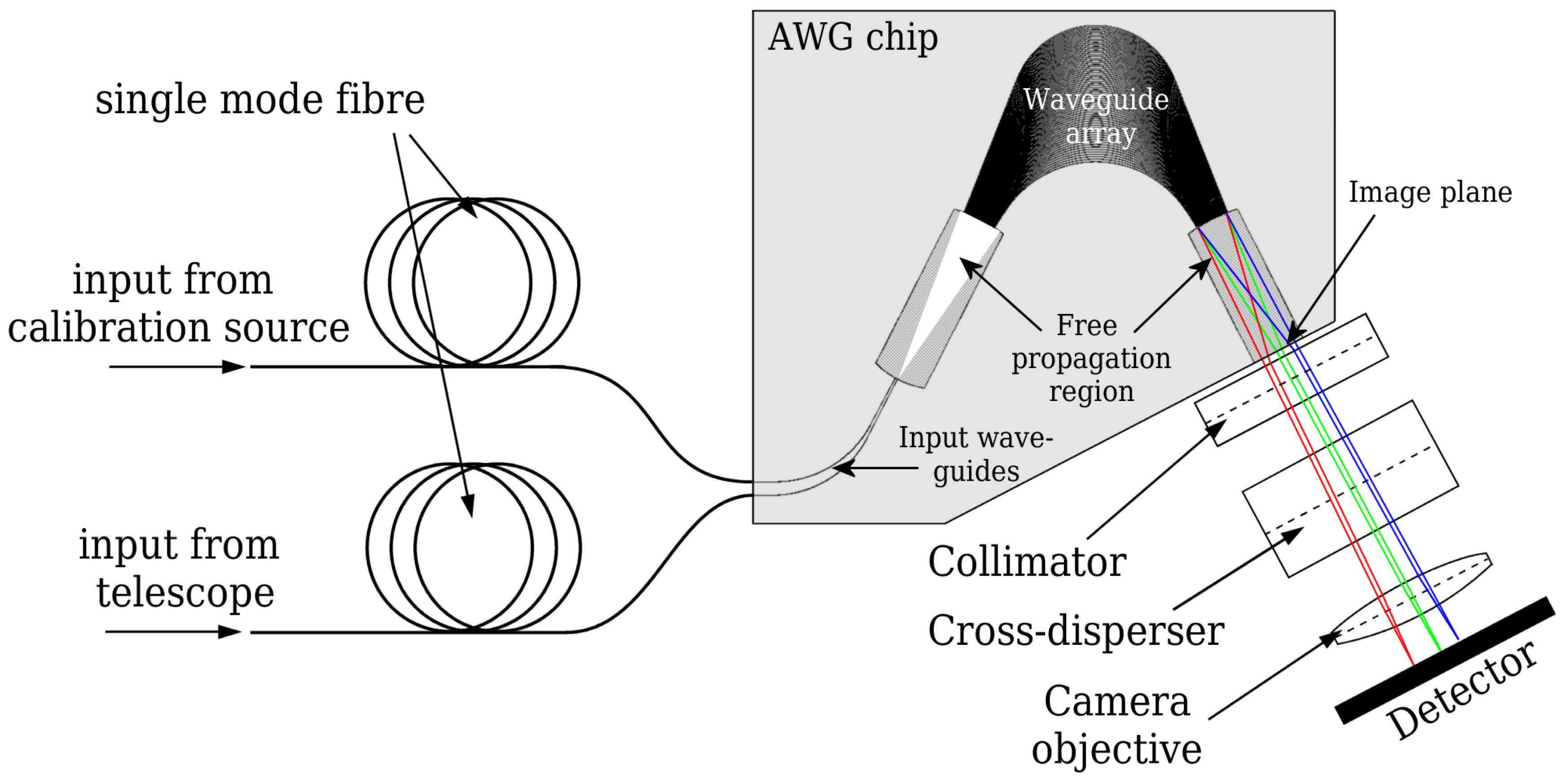
Figure 1. Schematic depiction of an arrayed-waveguide-grating (AWG)-based spectrograph assembly with cross-dispersive optics.
Photonics 04 00030 g001
Figure 2. Artificial example of a cross-dispersed AWG main spectrum with an interleaved reference.
Photonics 04 00030 g002
Figure 3. Cross-section of the rectangular buried channel waveguide core used in the AWG design. Core thickness is 3.5 μ m with variable core widths of 3.5 μ m (arrayed waveguides)—16.03 μ m (widest taper).
Photonics 04 00030 g003
Figure 4. Layout of the high-resolution AWG device.
Photonics 04 00030 g004
Figure 5. Input waveguide interface of the high-resolution AWG.
Photonics 04 00030 g005
Figure 6. Illustration of simulated coupling between the free propagation regions (FPR) and the waveguide array with standard linear tapers (left) and discontinuous MMI tapers (right). The beating pattern in the left image indicates two-mode interference. Waveguide core boundaries are highlighted in yellow colour.
Photonics 04 00030 g006
Figure 7. Comparison between the standard linear taper and the multimode interference (MMI) taper. Simulations were performed for TE and TM polarization in the wavelength range 1500 nm–1800 nm.
Photonics 04 00030 g007
Figure 8. Optical field amplitude at the AWG output facet for various RMS values.
Photonics 04 00030 g008
Figure 9. Simulation results for L = 24 mm (a); L = 18 mm (b); L = 12 mm (c); L = 6 mm (d).
Photonics 04 00030 g009
Figure 10. Figure of merit (FOM) maps for waveguide arrays of various sizes and propagation lengths. 800 waveguides, L = 10.5 cm (a); 600 waveguides, L = 8.3 cm (b); 400 waveguides, L = 6 cm (c); 200 waveguides, L = 3.8 cm (d).
Photonics 04 00030 g010
Table 1. Central input waveguide resolving powers and corresponding tapering widths.
λλ20 k25 k30 k35 k40 k45 k50 k55 k60 k
Width (μm)16.0312.4210.028.307.016.015.204.553.5
Location (μm)−8080−6060−4040−20200
Table 2. Critical thresholds of the refractive index distribution R M S for various values of L C and target resolving power R.
R60 k45 k30 k15 k
Lc
100 μ m 5.14 × 10 5 5.7 × 10 5 6.56 × 10 5 8 × 10 5
500 μ m 2 × 10 5 2.5 × 10 5 2.95 × 10 5 3.77 × 10 5
1000 μ m 1.52 × 10 5 1.7 × 10 5 2 × 10 5 3.2 × 10 5
3000 μ m 1.14 × 10 5 1.4 × 10 5 1.86 × 10 5 3.6 × 10 5