Abstract
In this paper, we numerically demonstrate a two-layer circular lattice photonic crystal fiber (PCF) biosensor based on the principle of surface plasmon resonance (SPR). The finite element method (FEM) with circular perfectly matched layer (PML) boundary condition is applied to evaluate the performance of the proposed sensor. A thin gold layer is deposited outside the PCF structure, which acts as the plasmonic material for this design. The sensing layer (analyte) is implemented in the outermost layer, which permits easy and more practical fabrication process compared to analyte is put inside the air holes. It is demonstrated that, at gold layer thickness of 40 nm, the proposed sensor shows maximum sensitivity of 2200 nm/RIU using the wavelength interrogation method in the sensing range between 1.33–1.36. Besides, using an amplitude interrogation method, a maximum sensitivity of 266 RIU−1 and a maximum sensor resolution of 3.75 × 10⁻⁵ RIU are obtained. We also discuss how phase matching points are varied with different fiber parameters. Owing to high sensitivity and simple design, the proposed sensor may find important applications in biochemical and biological analyte detection.
1. Introduction
In recent years, surface plasmon resonance (SPR) phenomenon has become a hot topic because of its widespread applications in multidisciplinary fields. SPR sensors exhibit high sensitivity characteristics, which enables a new window for numerous promising applications including biological sample detection, antibody-antigen interaction, medical diagnosis, organic-chemical sensing, food quality control, bioimaging, environment monitoring, and so on [1,2,3,4]. The idea of a surface plasmon (SP) phenomenon was first theoretically demonstrated by Ritchie et al. in the 1950s [5]. In 1983, SPR sensors were first introduced by Liedberg et al., which was on the basis of prism coupling [6]. The fundamental working principle of a prism coupling SPR sensor is based on the interaction of plasmonic materials and incident transverse magnetic (TM) or p-polarized light. The incident light (photons) has a certain frequency; when this frequency resembles that of the surface electrons of the plasmonic material, the p-polarized light stimulates the free electrons of the metal surface. Due to these collective oscillations, a surface plasmon wave (SPW) is originated in the metal–dielectric interface. Prism coupled-based biosensors are broadly employed because of the ease of usages. However, it is bulky and includes moving optical and mechanical parts, which limit its application in remote sensing [7].
Miniaturization of SPR-based sensors is necessary in order to reduce the sensor size and manufacturing costs. It is already known that photonic crystal fiber (PCF) exhibits unusual and appealing optical characteristics such as controllable birefringence, high confinement, and single mode propagation. [8]. Using these properties, it is possible to easily manipulate the evanescent field, which is a key parameter for controlling effective sensing performance. In contrast to prism coupling SPR sensors, PCF-based sensors provide tremendous design flexibility. Moreover, by tuning fiber structural parameters (e.g., pitch, air-hole dimension, and number of rings), sensitivity and sensing ranges can be enhanced. Fiber- or waveguide-based refractive index (RI) sensors including fiber Bragg gratings, long period fiber gratings, and micro-ring resonators are already available; however, the main limitations of these sensors are their low sensitivity and wide resonance peaks. Compared to fiber based sensors, SPR sensors provide very high sensitivity, i.e., a very small variation of an analyte’s RI can be detected from the large peak wavelength shift. Higher sensitivity results in better accuracy of the detection of an unknown analyte [9]. The selection of plasmonic material plays a key role in the performance of SPR sensors. Existing works on SPR sensors mostly use gold, silver, copper, and aluminum as the active plasmonic material [10]. Using silver material, it is possible to obtain a sharp resonance peak that increases sensing accuracy. However, silver is chemically unstable and has high susceptibility to oxidization, which reduces sensing performance [11]. Although a thin graphene layer coating can solve the oxidization issue, this additional coating increases fabrication problems and overall manufacturing cost. On the other hand, gold is chemically stable and does not easily oxidize [8]. Moreover, it also shows larger resonance peaks than other available plasmonic materials.
Researchers have carried out several distinct outcomes in order to improve the performance of SPR sensors. A SPR biosensor based on polymer PCF coated with metal oxide, where alternate holes in the second layer of the hexagonal lattice were coated with indium tin oxide (ITO), has been proposed [8]. Using the same structural configuration, another PCF has been reported, where a coated graphene-Ag bimetallic layer was used as the analyte channel [12]. A single hexagonal layer-based SPR sensor has been proposed by Gao et al., where a thin gold film and titanium dioxide (TiO2) layer were deposited in the outer wall of the air holes [13]. Very recently, graphene-silver deposited core-based SPR sensors with selectively filled analyte channels for RI detection have been proposed [14]. These internally metal film-coated SPR sensors suffer from major drawbacks. In terms of practical sensing, it is difficult to infiltrate the analyte in the inner air holes. Moreover, making a uniform metal coating inside the selective inner air holes makes the practical fabrication process more complex and cumbersome. To overcome these challenges, externally coated metallic film SPR sensors have been introduced. A square lattice D-shaped PCF RI sensor with a nanoscale gold film in the flat outer surface has been reported by Wang et al. [15]. Another hexagonal lattice D-shaped PCF sensor, where a gold layer was deposited on the flat surface to obtain SPR phenomena, has been proposed [16]. These types of PCFs require additional care during the removal of certain portions from the PCF to obtain flat surfaces. Moreover, realizing the practical fabrication for D-shaped PCFs is not feasible due to irregular geometry. Besides, graphene-Ag-based birefringent PCF has been demonstrated by Dash and Jha for RI sensing [17]. This PCF contains an irregular arrangement of air holes that is difficult to fabricate. Another study has been performed by Akowuah et al. for the detection of multichannel sensing [18]. This PCF contains elliptical air holes, which is impractical in terms of practical fabrication. Recently, plasmonic sensors based on metallic nanowire incorporated into the PCF have been experimentally reported using a thin pair of gold nanowires and a gold nanowire array [19,20]. Based on plasmonic resonance, metal-coated tapered fiber sensors have been also explored in the literature. The tapered fiber allows a unique platform to reduce the core and cladding diameter. A tapered single-mode fiber sensor with a small fiber diameter has been fabricated [21]. Moreover, ultrathin metallic nanolayer plasmonic tapered fiber with a small diameter of 20 µm has also been experimentally reported [22].
In this work, we propose a novel circular lattice air-hole PCF, which consists of two air-hole rings. The metal coating is deposited by a thin layer of gold, which is placed outside the PCF structure. This makes the detection process simpler and more straightforward because the analyte can be detected by just dropping it onto the outer surface. The proposed sensor shows a good figure of merit in terms of amplitude sensitivity, wavelength sensitivity, linearity, and sensor resolution. The circular pattern can be fabricated by using standard stack-and-draw, capillary stacking, and die-cast processes [23]. Additionally, we analyze the effect of varying the thickness of gold, pitch, and air-hole dimensions in order to obtain the best sensing performance.
2. Design Guidelines and Numerical Methods
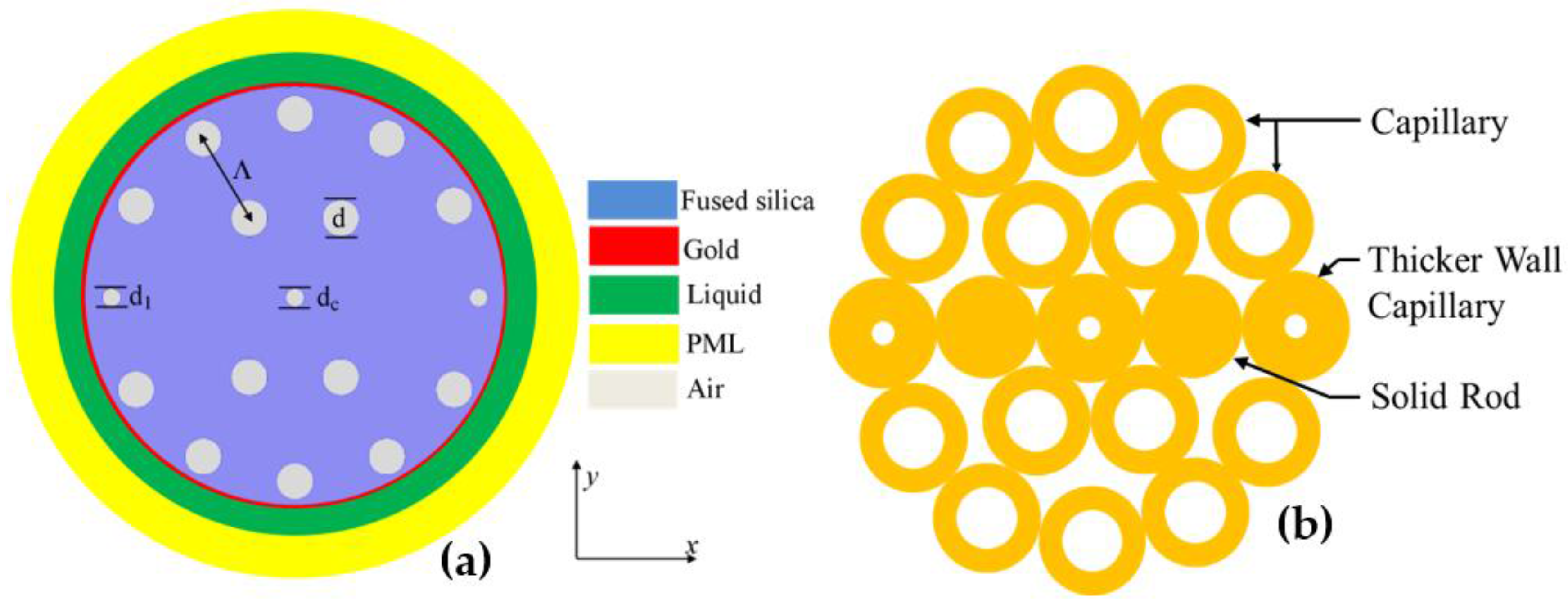
The cross-section view of the proposed circular lattice PCF sensor is shown in Figure 1a. It consists of two air-hole rings with two missing air holes in the first ring in order to create a birefringence effect. For the first ring of the circular lattice PCF, air holes are arranged at a 60° anticlockwise progressive rotation. The second ring is formed by a 30° anticlockwise progressive rotation of the air holes. It is worth noting that two air holes in the second ring together with the central hole are made relatively small. The reason is to accumulate the evanescent electromagnetic field at the two opposite sides of the PCF, which can easily stimulate the surface electrons. Here, Λ is the center-to-center distance between two adjacent air holes, dc is the diameter of central air hole, d1 is the diameter of smaller air holes, and d is the diameter of rest of the air holes. For the sake of structural simplicity, we made dc = d1. The stacked preform arrangement of the proposed PCF sensor is shown in Figure 1b.
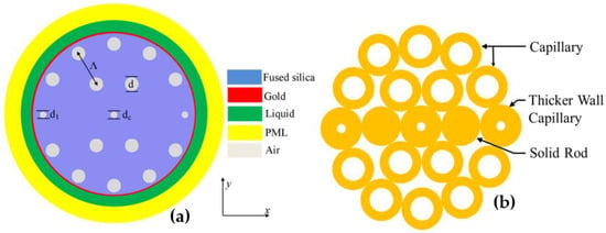
Figure 1.
(a) Cross-sectional view of the proposed circular lattice PCF sensor with Λ = 2 μm, dc = d1 = 0.2Λ, d = 0.4Λ, and tg = 40 nm. (b) Stacked preform of the proposed PCF.
The background material of the proposed sensor is fused silica. The refractive index of fused silica can be obtained from the Sellmeier equation [24]
where n is the wavelength dependent refractive index of fused silica, and λ is the wavelength in µm. B1, B2, B3, C1, C2, and C3 are the Sellmeier constants. For fused silica, the constants are 0.69616300, 0.407942600, 0.897479400, 0.00467914826, 0.0135120631, and 97.9340025, respectively. Here, tg represents the fixed thickness of the gold layer, which is deposited on the outer surface of the PCF. For this design, we kept tg = 40 nm. We used the Drude-Lorentz model to obtain the dielectric constant of the gold, and this model is characterized by the following equation [25]:
where εAu is the permittivity of gold, ε∞ is the permittivity at high frequency with a value of 5.9673, ω is the angular frequency, which is given by ω = 2πc/λ, c is the velocity of light in vacuum, ωD is the plasma frequency, and γD is the damping frequency. Here, ωD/2π = 2113.6 THz, γD/2π = 15.92 THz, and the weighting factor Δε = 1.09. The spectral width and oscillator strength of the Lorentz oscillators are given by ΓL/2π = 104.86 THz and ΩL/2π = 650.07 THz, respectively.
It is a challenging task to obtain a uniform thickness of the outer gold layer coated on the circular surface of the PCF. There are several methods including radio frequency (RF) sputtering, thermal evaporation, and wet-chemistry deposition that can be implemented to deposit this outer thin layer [26]. However, these normal metal coating methods suffer from extreme surface roughness. Considering this fact, chemical vapor deposition (CVD) [27] is an efficient method that offers uniform nanolayer coating with minimal surface roughness. Metal nanoparticles can also be used by maintaining their size during fabrication to obtain a thin and smooth coating surface [26]. The simulation results were carried out by using finite element method (FEM)-based COMSOL software. We imposed a circular perfectly matched layer (PML) and scattering boundary conditions in order to absorb the outgoing waves from the surface of the PCF. The thickness of the PML was selected by the convergence test, where several simulations were performed with different PML thickness. A constant liquid layer thickness of 1.6 µm was used throughout the simulation. Besides, the element size of the mesh was kept as small as possible so that smaller air holes can be mapped easily. The complete commutation domain took 45,476 triangular elements and 2136 vertex elements.
3. Simulation Results and Performance Analysis
The fundamental operating mechanism of PCF-based SPR sensors depends on the mutual interaction between evanescent field and surface electrons, which occurs in the metal–dielectric interface. Due to this phenomenon, SPW that interacts with the sensing layer is generated. The performance of the SPR sensors depends on the geometrical parameters of the PCF. These parameters should be selected in such a way that offers an easy interaction of the evanescent field with the metal surface. The target property is to increase the sensitivity by making a strong coupling between core-guided mode and SPP mode. First, we select the value of dc at 0.2Λ. If we set a value of dc larger than 0.2Λ, that would reduce the effective refractive index (neff) of the core and deteriorate the guidance along the core [17]. On the other hand, a smaller value of dc would result in strong light confinement in the core that effectively reduces the generation of SPW. The value of d1 was selected at 0.2Λ so that the evanescent field can easily pass towards a metallic layer. A larger value than 0.2Λ could prevent the efficient interaction with the sensing layer. We used d1 = dc, thereby reducing the number of degrees of freedom in the proposed PCF. Additionally, the value of d was kept as 0.4Λ. The reason for choosing comparatively larger air holes is to reduce the light confinement in the metal–dielectric interface [8]. In the entire simulation, the design parameters (Λ = 2 μm, dc = d1 = 0.2Λ, d = 0.4Λ, tg = 40 nm) are kept constant in order to obtain the best sensing performance.
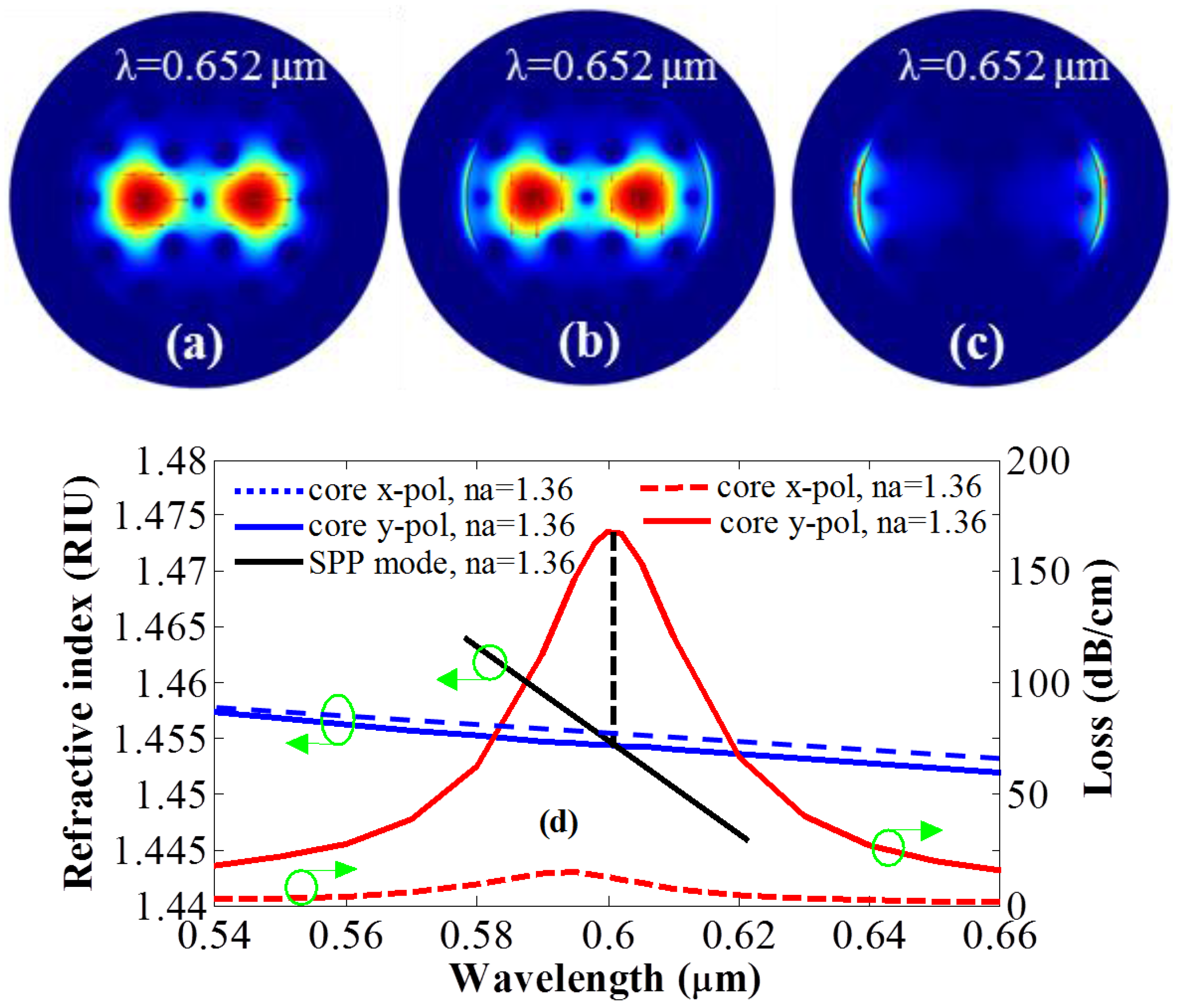
The mode field profiles of fundamental x-polarization and y-polarization modes and y-polarization of the SPP mode are shown in Figure 2a–c, respectively. The proposed fiber shows birefringence due to two missing air holes, which induces an effective index difference between the fundamental x-polarization and y-polarization modes. As illustrated in Figure 2b, y-polarization mode shows stronger electric field near the metal surface; therefore, the evanescent field can easily interact with the outer sensing layer compared to the fundamental x-polarization mode (shown in Figure 2a). As a result, the fundamental y-polarization mode is strongly coupled with the surface electrons of gold.
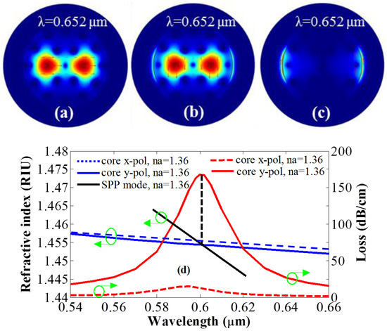
Figure 2.
Mode field distribution of fundamental (a) x-polarization core mode, (b) y-polarization core mode, and (c) y-polarization SPP mode at 0.652 µm. (d) Dispersion relation between the fundamental core-guided mode and SPP mode with na = 1.36 and tg = 30 nm.
Figure 2d shows the neff of core-guiding mode, the surface plasmon polariton (SPP) mode, and the loss spectra of the fundamental x-polarization and y-polarization modes with analyte RI (na) of 1.36. The effective refractive index of fundamental y-polarized SPP mode was taken from the simulation software for different operating wavelengths. The effective refractive indices were plotted as a function of wavelength to obtain the dispersion curve for SPP mode. The SPP curve is shown in Figure 2d indicated by a solid black line. It can be evident that, at 0.6 μm, the real part of the neff of the fundamental y-polarization mode and the SPP mode coincide with each other. This is known as the resonance or phase matching condition, and the operating wavelength (in this case 0.6 μm) is known as resonance wavelength. At this wavelength, a sharp peak is observed that represents the maximum energy transfer from core-guided mode to the SPP mode. The dispersion relation between the core-guided mode and the SPP mode is shown in Figure 2d. From this figure, it can be also concluded that the fundamental y-polarization mode shows a higher and sharper resonance peak than that of the fundamental x-polarization mode. Due to the very low loss depth of the fundamental x-polarization, in the rest of the study, we only considered the fundamental y-polarization mode for the performance analysis.
Confinement loss plays a vital role in the evaluation of the sensor’s performance, and this parameter can be obtained by using the following equation [28]:
where k0 = 2π/λ is the wave number in the free space, λ is the operating wavelength, and Im(neff) is the imaginary part of the effective refractive index.
The real part of the neff of the SPP mode is highly dependent on the small variation of analyte RI. A slight variation of analyte RI results in a change of neff, which is responsible for the shift in the phase matching point towards other resonance wavelengths. Figure 3a shows the phenomena of the changing phase matching points due to the variation of na from 1.33 to 1.36. As clearly demonstrated from the figure, increasing the value of analyte RI causes red shifting, i.e., resonance wavelength shift towards a higher wavelength. When RI of analyte is increased, it turns to shift the real part of the neff of the SPP mode in Figure 2d towards a higher value. As a consequence, the resonance wavelength is increased towards higher wavelength. Due to the change of na from 1.33 to 1.34, from 1.34 to 1.35, and from 1.35 to 1.36, resonance wavelengths are shifted to 0.6–0.61 µm, 0.61–0.63 µm, and 0.63–0.652 µm, respectively, with tg = 40 nm. It can be observed from Figure 3a that loss depth can be increased by increasing the analyte RI. Increasing the value of na leads to a reduction of the index contrast between the core and cladding, which leads to an increase in confinement loss. The lowest confinement loss of 66 dB/cm was found for an analyte RI of 1.33, where a broadening of the resonance spectrum was also observed. The maximum loss peak was observed at 0.652 µm, which is 157 dB/cm for an analyte RI of 1.36.

Figure 3.
(a) Fundamental loss variation for increasing analyte RI from 1.33 to 1.36 and (b) amplitude sensitivity for different analyte RI with Λ = 2 μm, dc = d1 = 0.2Λ, d = 0.4Λ, and tg = 40 nm.
The performance of the PCF-based SPR sensor can be measured by the sensitivity. We analyzed the sensitivity of the proposed fiber by using wavelength interrogation and amplitude interrogation. In wavelength interrogation, wavelength sensitivity can be computed by the following formula [14]:
where Δλpeak is the difference between peak wavelength shifts and Δna is the variation of analyte RI. The proposed fiber shows a Δλpeak of 10 nm, 20 nm, and 22 nm for Δna of 0.01, where changes in the analyte RI are 1.33–1.34, 1.34–1.35, and 1.35–1.36. Thus, the calculated wavelength sensitivities are 1000, 2000, and 2200 nm/RIU, respectively. The maximum wavelength sensitivity, i.e., 2200 nm/RIU is comparable with previously proposed results [8,12,18,28]. The resolution of the sensor is another important parameter that represents how a small change of analyte RI can be detected by the sensor. The resolution of the proposed sensor can be obtained by the given formula [15]:
Assuming that Δna = 0.01, Δλmin = 0.1, and Δλpeak = 22 nm, we found the resolution of the proposed sensor to be as high as 4.55 × 10⁻⁵, which is comparable with [8,12,16,18,28]. Therefore, any small change in analyte RI in the order of 10−5 can be detected with a high degree of accuracy.
The wavelength interrogation method requires spectral manipulation to obtain sensitivity that makes detection process complex. On the other hand, amplitude interrogation can solve this issue by measuring sensitivity at a specific wavelength. The amplitude sensitivity can be obtained by the following equation [28]:
where α(λ,na) is the overall propagation loss at RI of na, and ∂α(λ,na) is the loss difference between two loss spectra. Figure 3b depicts the amplitude sensitivity of the proposed sensor for different analyte RI values. We found a maximum amplitude sensitivity of about 266 RIU−1 at 0.655 µm for an analyte RI of 1.35. Moreover, an amplitude sensitivity of about 185 and 241 RIU−1 was obtained for analyte RI values of 1.34 and 1.36, respectively. In this case, the designed sensor provides a maximum sensor resolution of 3.75 × 10⁻⁵ by assuming that a 1% change of the transmitted intensity is detectable.
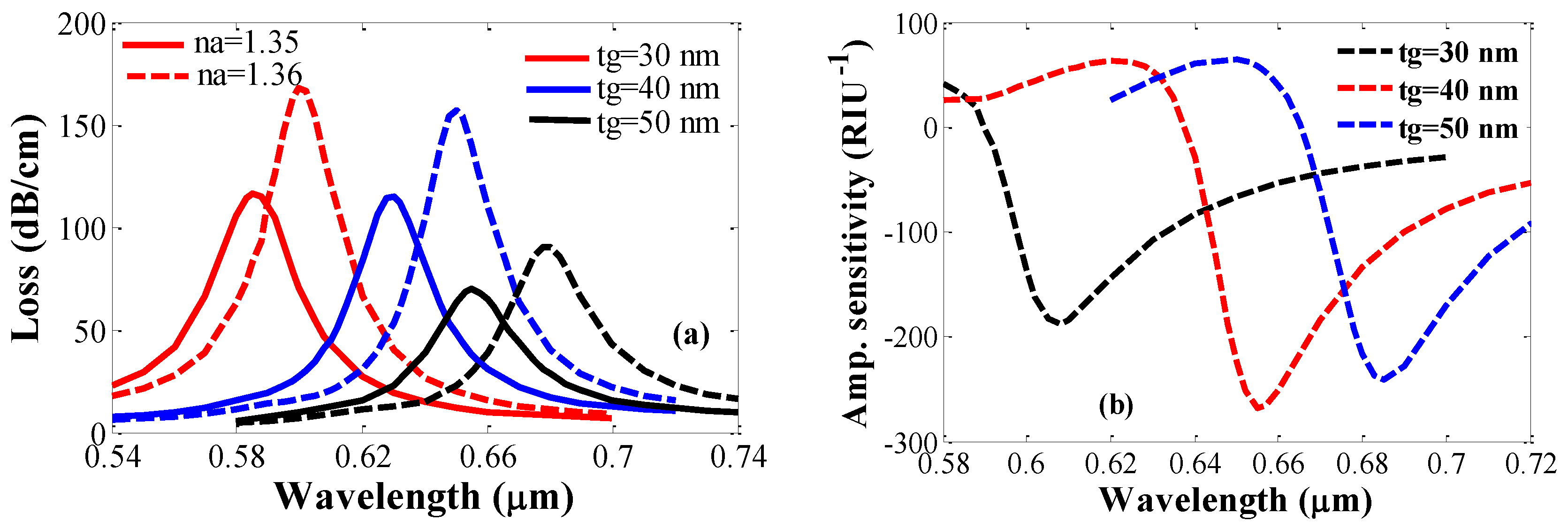
There are significant impacts of loss depth and amplitude sensitivity on the variation of gold layer thickness. In Figure 4a, loss spectra for different gold thickness are shown with analyte RI values of 1.35 and 1.36, respectively. As depicted in the figure for a fixed analyte RI, increasing the gold thickness reduces loss depth. The reason is the higher damping loss due to the increase in gold layer thickness. Moreover, increasing gold thickness causes a shifting of the peak loss towards a longer wavelength. Amplitude sensitivity as a function of wavelength for different gold layer thicknesses is shown in Figure 4b. It is evident that the proposed sensor shows amplitude sensitivities of 188, 266, and 241 RIU−1 for thicknesses of 30, 40, and 50 nm, respectively. Since maximum sensitivity can be achieved by setting tg of 40 nm. Therefore, throughout the analysis, tg = 40 nm was used to ensure better sensing performance.
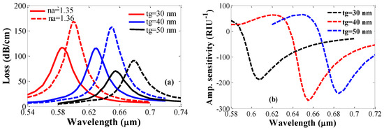
Figure 4.
(a) Fundamental loss variation of the proposed sensor for different gold layer thicknesses and (b) amplitude sensitivity for different gold layer thicknesses with Λ = 2 μm, dc = d1 = 0.2Λ, and d = 0.4Λ for an analyte RI of 1.35.
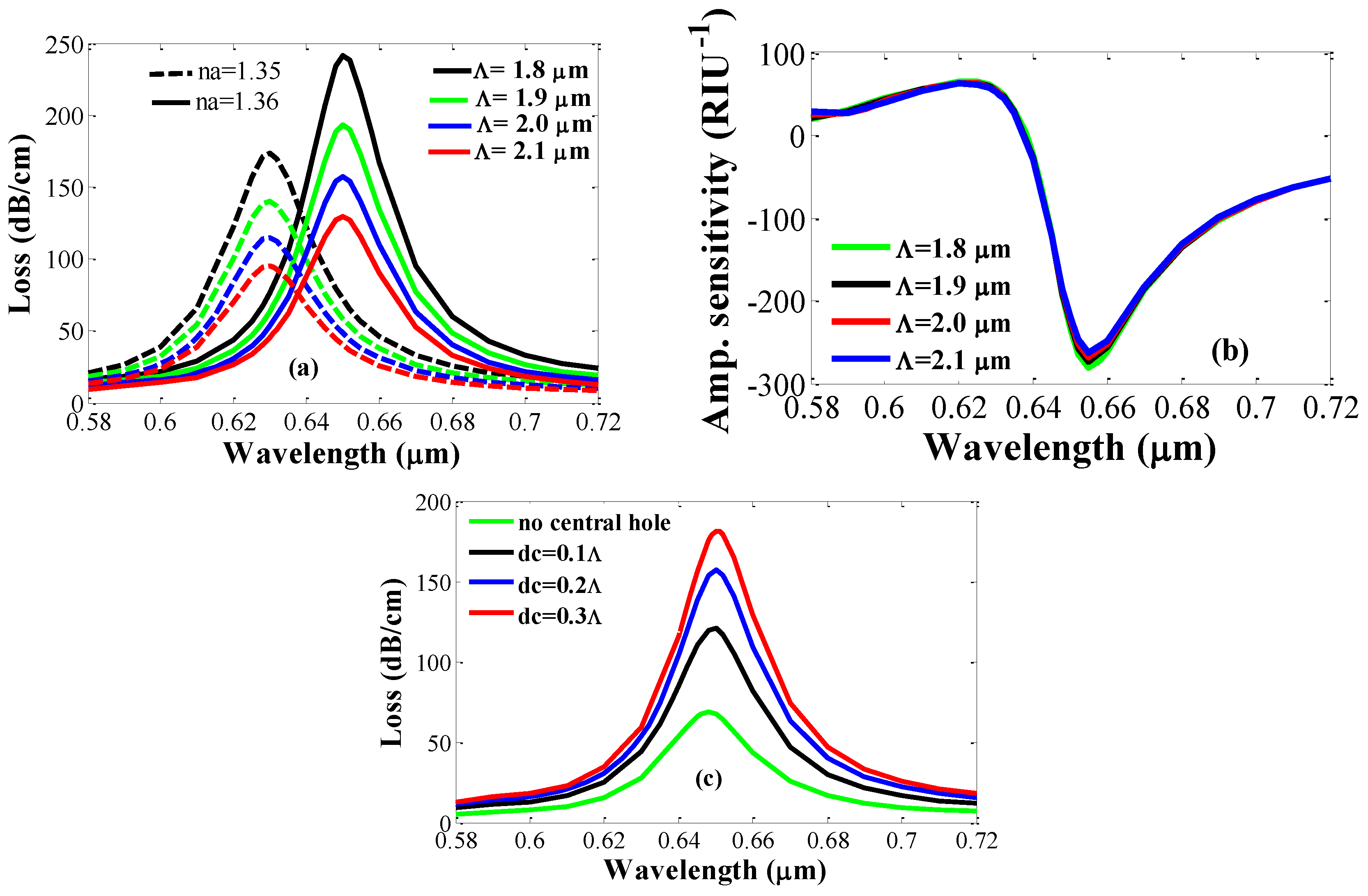
A changing pitch and diameter of the central air hole significant affects confinement loss. Loss spectra and sensitivity of the proposed sensor for the changing pitch values are illustrated in Figure 5a,b. As the pitch values are increased from 1.8 to 2.1 µm, loss depth reduces from 242 to 130 dB/cm for an analyte RI of 1.36. Due to pitch change, no peak loss shift was observed for a fixed analyte RI. The proposed sensor shows almost identical sensitivity for pitch values between 1.8 and 2.1 µm. On the other hand, the diameter of the central air hole is varied from null to 0.3Λ for an analyte RI of 1.36, and the results are shown in Figure 5c. When no central air hole is used, we found a loss depth of 68 dB/cm. At dc = 0.3Λ, the loss depth increases to 182 dB/cm. Unlike the pitch results, an enlarging central air-hole diameter causes an increase in loss depth. Therefore, the pitch and diameter of the central air hole should be chosen in such a way that the best sensing performance is confirmed. Considering this fact, we used Λ = 2 μm and dc = 0.2Λ in the entire analysis of the proposed sensor.
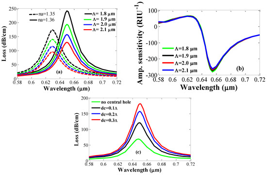
Figure 5.
(a) Fundamental loss spectrum for increasing pitch values from 1.8 to 2.1 µm; (b) amplitude sensitivity for different pitch values with an analyte RI of 1.35; (c) loss spectrum for different central air-hole diameter with d = 0.4Λ and t = 40 nm with an analyte RI of 1.36.
In real-world sensing applications, a sensor generally operates at a fixed wavelength. Therefore, it is necessary to discuss the dependence of the amplitude sensitivity as a function of various geometrical parameters such as pitch and air-hole diameters. Figure 6a shows the effect of a changing pitch value on amplitude sensitivity at a fixed wavelength of 0.655 µm for an analyte RI of 1.35. As illustrated in the figure, amplitude sensitivity gradually decreases with increasing pitch. It should be noted that amplitude sensitivity is calculated by varying pitch only while other parameters are kept constant. The dependence of changing the air-hole diameter (d and d1) on amplitude sensitivity is shown in Figure 6b, with a fixed wavelength of 0.655 µm and an analyte RI of 1.35. As seen from the figure, increasing the value of d results in no significant change in amplitude sensitivity. The variation of amplitude sensitivity with increasing d1 is also shown in the inset. It can be found that increasing d1 from 0.3 to 0.5 µm changes amplitude sensitivity from 268 to 261 RIU−1.

Figure 6.
Variation of amplitude sensitivity due to the change of (a) pitch values from 1.8 to 2.2 μm and (b) air-hole diameter, d from 0.6 to 1 μm and d1 from 0.3 to 0.5 μm at a fixed wavelength of 0.655 μm.
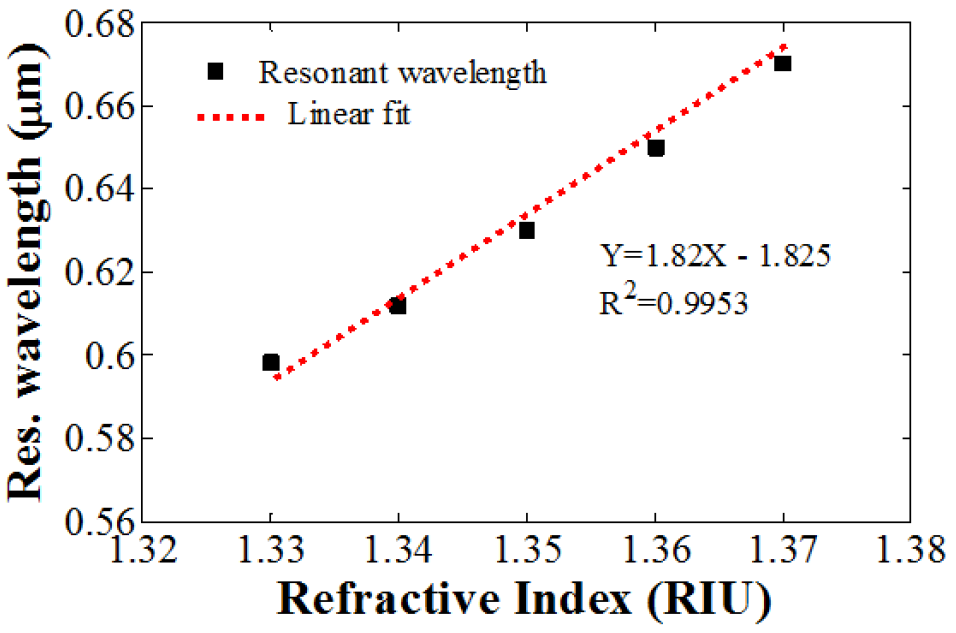
A good sensor should have high linearity response. The linear fitting of the resonance wavelength with varying analyte RI values from 1.33 to 1.36 is shown in Figure 7. The regression equation of the linear line fitting is given by Y = 1.82X − 1.825, where Y indicates the resonance wavelength and X indicates analyte RI. The R-square value for the linear line fitting is 0.9953, which indicates very good linearity. Due to good line fitting characteristics, the proposed sensor can be implemented for practical RI detection.
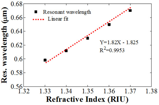
Figure 7.
Linear fitting of the resonance wavelength as a function of analyte RI for Λ = 2 μm, dc = d1 = 0.2Λ, d = 0.4Λ, and tg = 40 nm.
In practical applications, the fluctuation of input light intensity is interrupted so that the exact value of amplitude sensitivity can be obtained. Due to the change in input intensity, the amplitude sensitivity varies. The geometric parameters of the PCF determine the transmitted and reflected waves (S-parameter). In this study, we mainly focus on the transmittance of the guided mode, i.e., the evanescent field. The diameter of the air holes and pitch values determine how much the evanescent field propagates towards the metal interface. In the case of the proposed PCF, the central air hole is required to prohibit the light wave centered in the core, which could reduce the chances of reaching the metal interface. On the other hand, d1 is kept as low as possible since smaller air holes provide enough space to guide the evanescent field. Thus, the transmittance of the evanescent field increases. Furthermore, d is kept comparatively large, which ensures that the evanescent field is guided in the two opposite directions along the x-axis. It also increases the transmittance of the proposed sensor, which significantly increases the amplitude sensitivity.
The proposed PCF can be fabricated by the standard stack-and-draw method [29]. The designed PCF has only two rings, and the pitch size is 2 µm; as a result, it has small diameter of around 10 µm. However, the standard PCF size is 125 µm. Our proposed PCF can be realized in two different ways: (1) by using external silica solid-rods and mixing them with the background material of fused silica after applying vacuum during the fabrication; and (2) jacketing the proposed PCF 2–3 times. In case of the proposed PCF, a large solid silica surface will be formed outside of the cladding. This is the similar phenomenon as illustrated in [30]. Later on, by polishing the PCF surface we can achieve the proposed PCF. Additionally, the proposed PCF size can also be achieved by following the tapering technique [31].
4. Conclusions
We propose a highly sensitive circular lattice PCF-based SPR sensor for the detection of unknown analytes. The numerical investigations were performed by using FEM with PML and scattering boundary conditions. The thin layer of gold and analyte were both placed at the outer surface of the PCF, which permitted easy fabrication and more practical detection. The proposed sensor shows a maximum sensitivity of 266 RIU−1, which yields a maximum resolution of 3.75 × 10⁻⁵ RIU. Moreover, loss depth variations for different gold layer thicknesses, analyte RI values, pitch values, and central air-hole diameters are also rigorously discussed. Due to high sensitivity and high linearity, the proposed PCF SPR sensor can be considered ideal for refractive index detections.
Author Contributions
M.R. Hasan and A.A. Rifat conceived the design; M.R. Hasan and S.A. Emi performed the simulations; M.R. Hasan and S. Ali analyzed the simulation data; M.R. Hasan wrote the paper; M.R. Hasan, A.A. Rifat and S. Rana made revisions and finalized the paper.
Conflicts of Interest
The authors declare no conflict of interest.
References
- Berger, C.E.; Greve, J. Differential SPR immune sensing. Sens. Actuators B Chem. 2000, 63, 103–108. [Google Scholar] [CrossRef]
- Zhao, Y.; Deng, Z.-Q.; Li, J. Photonic crystal fiber based surface plasmon resonance chemical sensors. Sens. Actuators B Chem. 2014, 202, 557–567. [Google Scholar] [CrossRef]
- Silva, S.; Rozia, P.; Frazoa, O. Refractive index measurement of liquids based on microstructured optical fibers. Photonics 2014, 1, 516–529. [Google Scholar] [CrossRef]
- Jorgenson, R.; Yee, S. A fiber-optic chemical sensor based on surface plasmon resonance. Sens. Actuators B Chem. 1993, 12, 213–220. [Google Scholar] [CrossRef]
- Ritchie, R. Plasma losses by fast electrons in thin films. Phys. Rev. 1957, 106, 874. [Google Scholar] [CrossRef]
- Liedberg, B.; Nylander, C.; Lunström, I. Surface plasmon resonance for gas detection and biosensing. Sens. Actuators 1983, 4, 299–304. [Google Scholar] [CrossRef]
- Gupta, B.D.; Verma, R.K. Surface plasmon resonance-based fiber optic sensors: Principle, probe designs, and some applications. J. Sens. 2009, 2009, 979761. [Google Scholar] [CrossRef]
- Qin, W.; Li, S.; Yao, Y.; Xin, X.; Xue, J. Analyte-filled core self-calibration microstructured optical fiber based plasmonic sensor for detecting high refractive index aqueous analyte. Opt. Lasers Eng. 2014, 58, 1–8. [Google Scholar] [CrossRef]
- Gupta, B.D.; Sharma, A.K. Sensitivity evaluation of a multi-layered surface plasmon resonance-based fiber optic sensor: A theoretical study. Sens. Actuators B Chem. 2005, 107, 40–46. [Google Scholar] [CrossRef]
- McPeak, K.M.; Jayanti, S.V.; Kress, S.J.; Meyer, S.; Iotti, S.; Rossinelli, A. Plasmonic films can easily be better: Rules and recipes. ACS Photonics 2015, 2, 326–333. [Google Scholar] [CrossRef] [PubMed]
- Lu, Y.; Hao, C.J.; Wu, B.Q.; Musideke, M.; Duan, L.C.; Wen, W.Q.; Yao, J.Q. Surface plasmon resonance sensor based on polymer photonic crystal fibers with metal nano layers. Sensors 2013, 13, 956–965. [Google Scholar] [CrossRef] [PubMed]
- Yang, X.; Lu, Y.; Liu, B.; Yao, J. Analysis of Graphene-Based Photonic Crystal Fiber Sensor Using Birefringence and Surface Plasmon Resonance. Plasmonics 2016, 1–8. [Google Scholar] [CrossRef]
- Gao, D.; Guan, C.; Wen, Y.; Zhong, X.; Yuan, L. Multi-hole fiber based surface plasmon resonance sensor operated at near-infrared wavelengths. Opt. Commun. 2014, 313, 94–98. [Google Scholar] [CrossRef]
- Rifat, A.A.; Mahdiraji, G.A.; Chow, D.M.; Shee, Y.G.; Ahmed, R.; Adikan, F.R.M. Photonic Crystal Fiber-Based Surface Plasmon Resonance Sensor with Selective Analyte Channels and Graphene-Silver Deposited Core. Sensors 2015, 15, 11499–11510. [Google Scholar] [CrossRef] [PubMed]
- Wang, G.; Li, S.; An, G.; Wang, X.; Zhao, Y.; Zhang, W.; Chen, H. Highly sensitive D-shaped photonic crystal fiber biological sensors based on surface plasmon resonance. Opt. Quantum Electron. 2016, 48, 1–9. [Google Scholar] [CrossRef]
- Gangwar, R.K.; Singh, V.N. Highly sensitive surface plasmon resonance based D-shaped photonic crystal fiber refractive index sensor. Plasmonics 2016, 1–6. [Google Scholar] [CrossRef]
- Dash, J.N.; Jha, R. Graphene-Based Birefringent Photonic Crystal Fiber Sensor Using Surface Plasmon Resonance. IEEE Photonics Technol. Lett. 2014, 26, 1092–1095. [Google Scholar] [CrossRef]
- Akowuah, E.K.; Gorman, T.; Ademgil, H.; Haxha, S.; Robinson, G.K.; Oliver, J.V. Numerical analysis of a photonic crystal fiber for biosensing applications. IEEE J. Quantum Electron. 2012, 48, 1403–1410. [Google Scholar] [CrossRef]
- Lee, H.W.; Schmidt, M.A.; Russell, P.S. Excitation of a nanowire “molecule” in gold-filled photonic crystal fiber. Opt. Lett. 2012, 37, 2946–2948. [Google Scholar] [CrossRef] [PubMed]
- Uebel, P.; Schmidt, M.A.; Lee, H.W.; Russell, P.S. Polarisation-resolved near-field mapping of a coupled gold nanowire array. Opt. Express 2012, 20, 28409–28417. [Google Scholar] [CrossRef] [PubMed]
- Diez, A.; Andres, M.V.; Cruz, J.L. In-line fiber-optic sensors based on the excitation of surface plasma modes in metal-coated tapered fibers. Sens. Actuators B Chem. 2001, 73, 95–99. [Google Scholar] [CrossRef]
- Wieduwilt, T.; Tuniz, A.; Linzen, S.; Goerke, S.; Dellith, J.; Hübner, U.; Schmidt, M.A. Ultrathin niobium nanofilms on fiber optical tapers–A new route towards low-loss hybrid plasmonic modes. Sci. Rep. 2015, 5, 17060-1–17060-12. [Google Scholar] [CrossRef] [PubMed]
- Zhou, G.; Hou, Z.; Li, S.; Hou, L. Fabrication of glass photonic crystal fibers with a die-cast process. Appl. Opt. 2006, 45, 4433–4436. [Google Scholar]
- Hasan, M.R.; Hasan, M.I.; Anower, M.S. Tellurite glass defectcore spiral photonic crystal fiber with low loss and large negative flattened dispersion over S + C + L + U wavelength bands. Appl. Opt. 2015, 54, 9456–9461. [Google Scholar] [CrossRef] [PubMed]
- Vial, A.; Grimault, A.-S.; Macías, D.; Barchiesi, D.; de La Chapelle, M.L. Improved analytical fit of gold dispersion: Application to the modeling of extinction spectra with a finite-difference time-domain method. Phys. Rev. B 2005, 71, 085416. [Google Scholar] [CrossRef]
- Rifat, A.A.; Ahmed, R.; Yetisen, A.K.; Butt, H.; Sabouri, A.; Mahdiraji, G.A.; Yun, S.H.; Adikan, F.R. Photonic crystal fiber based plasmonic sensors. Sens. Actuators B Chem. 2017, 243, 311–325. [Google Scholar] [CrossRef]
- Malinský, P.; Slepicka, P.; Hnatowicz, V.; Švorcík, V. Early stages of growth of gold layers sputter deposited on glass and silicon substrates. Nanoscale Res. Lett. 2012, 7, 241-1–241-7. [Google Scholar]
- Rifat, A.A.; Mahdiraji, G.A.; Ahmed, R.; Chow, M.D.; Sua, Y.M.; Shee, Y.G. Copper-graphene based photonic crystal fiber plasmonic biosensor. IEEE Photonics J. 2016, 8, 4800408. [Google Scholar] [CrossRef]
- Mahdiraji, G.A.; Chow, D.M.; Sandoghchi, S.; Amirkhan, F.; Dermosesian, E.; Yeo, K.S.; Kakaei, Z.; Ghomeishi, M.; Poh, S.Y.; Gang, S.Y.; et al. Challenges and solutions in fabrication of silica based photonic crystal fibers: An experimental study. Fiber Int. Opt. 2014, 33, 85–104. [Google Scholar] [CrossRef]
- Chen, Y.S.; Yan, P.G.; Chen, H.; Liu, A.J.; Ruan, S.C. Harmonic mode-locked fiber laser based on photonic crystal fiber filled with topological insulator solution. Photonics 2015, 2, 342–354. [Google Scholar] [CrossRef]
- Chandalia, J.K.; Eggleton, B.J.; Windeler, R.S.; Kosinski, S.G.; Liu, X.; Xu, C. Adiabatic coupling in tapered air–silica microstructured optical fiber. IEEE Photonics Technol. Lett. 2001, 13, 52–54. [Google Scholar] [CrossRef]
© 2017 by the authors. Licensee MDPI, Basel, Switzerland. This article is an open access article distributed under the terms and conditions of the Creative Commons Attribution (CC BY) license ( http://creativecommons.org/licenses/by/4.0/).

