1. Introduction
In drug discovery, one of the most time-consuming stages is the identification of candidate drugs. Modern high-content screening (HCS) microscopes process thousands of living cell samples, which have been treated with varied dosages of drug leads. The resulting images are analyzed by advanced algorithms to determine the drug effectiveness and dosage optimization [
1]. These results are analyzed for imaging phenotypes related to the cell’s morphology and proliferation rate, as a means of determining the underlying reaction to the drug [
2]. While important discoveries can be made through these phenotypes, it is impossible to determine the exact nature of how the drug is affecting the cell line.
Inside a cell, a complex interaction network of proteins exists to maintain homeostasis and regulate cell behavior [
3]. Whether it is two proteins binding to each other or multiple proteins forming an oligomer, these protein-protein interactions happen at the scale of a few nanometers: far below the optical diffraction limit. Consequently, such interactions are invisible in morphological high-content screening. More insight can be obtained if a more direct approach to monitoring protein-protein interactions is used in HCS. Such techniques use existing information of these interactions, as well as their biological pathways, to enable a better understanding of how the drug works, as well as the side effects. One such directed approach is to use Förster resonance energy transfer (FRET), which offers the ability to qualitatively and quantitatively monitor molecular interactions at nanometer scales. FRET is a phenomenon whereby an excited “donor” fluorophore non-radiatively transfers its excitation energy to a nearby “acceptor” fluorophore, which then fluoresces as it returns to the ground state. The proximity of the two fluorophores must be on the scale of <10 nm, which makes it suitable for tagging a specific protein-protein interaction [
4]. While FRET can be monitored, to some degree, by measuring the ratio of donor emission to acceptor emission (“intensity FRET”), this method has complications, due to the differing local populations of donor and acceptor fluorophores and spectral bleeding effects between the excitation and emission spectra of the FRET pair [
4,
5]. Polarization-resolved FRET can be performed with a very good signal-to-noise ratio [
6], but is complicated by losses and distortions due to polarization [
7]. It also is not good at distinguishing between varying degrees of FRET [
7].
Fluorescence lifetime imaging microscopy can measure FRET (FLIM-FRET), through monitoring the reduction in the fluorescence lifetime of the donor fluorophore. FLIM-FRET does not have the abovementioned complications, making it a more accurate measure of FRET activity—subsequently protein-protein interaction—within the cell. At the same time, fluorescence lifetime is also inherently more challenging to measure, however, since the targeted lifetimes are on the scale of 1–10 ns and the requirement of resolving the lifetime changes to a few hundreds of picoseconds. Furthermore, each pixel of an image could have many of the proteins of interest with differing degrees of FRET interaction. In the simplified case where both interacting and non-interacting fluorophores contribute to the same pixel, the fluorescence signal of the pixel would be a biexponential decay [
8].
Time-correlated single-photon counting (TCSPC) is the gold standard by which FLIM is performed [
9]. The principle is to measure the arrival times of each photon with very high precision, and form a histogram of arrival times as the fluorescence decay curve. This method requires the use of very low emission light levels in order to ensure that only a maximum of one photon arrives for each repetition, with the rule-of-thumb being a collection rate never exceeding 5% of the repetition rate [
10]. Dividing the signal between multiple detectors and TCSPC circuits can proportionally improve the maximum allowable collection rate [
11]. The method uses a raster scanning (confocal or multiphoton) approach, where each spot of the image is measured sequentially, with the signal being collected by a photomultiplier tube or single-photon avalanche diode (SPAD) [
12]. Understandably, this makes TCSPC a challenge to apply to HCS, where a high priority is placed on acquisition throughput.
FLIM is also measured by time-gated imaging, where intensified charge-coupled device imagers (ICCDs) are made active for only a short time window [
10,
13]. By measuring multiple time windows over repeated excitations, an approximation of the fluorescence lifetime curve can be generated. Due to the large gate width (>300 ps), the ICCD gating is not able to achieve a suitably high time resolution in order to separate the components of biexponential decays. Typically, this technique only measures two time windows, and uses their ratio to measure an average fluorescence lifetime [
13]. For a biexponential fluorescence decay, this is not ideal in determining the ratio of binding to non-binding FRET pair populations measured from a spot in the image. It is also a wide-field imaging technique, which not only affects the ability to resolve subcellular features, but also means that each decay represents a larger volume of the sample (including out-of-focus contributions), greatly reducing the precision of the FRET measurement [
14]. Finally, it is a slow technique, due to the rejection of photons arriving outside of the time window, and the inherently low quantum efficiency of the image intensifier. FLIM can also be measured through frequency domain analysis. In its most common implementation, a modulated ICCD is used to collect phase and attenuation information at different frequencies [
15], but this method suffers similar drawbacks as the time-domain gated-ICCD approach discussed previously.
While gated imaging and other analog approaches are faster and can be easier to implement, TCSPC is the most sensitive method of acquiring fluorescence decays, due to the discrete photon-counting nature that offers excellent signal-to-noise ratios [
16]. This is especially important in the case of live cell imaging, where the number of available photons in severely limited because low illumination intensities must be used since fluorophores are irreversibly photobleached after excitation [
17].
In order to achieve a suitable effective spatial resolution and optical sectioning, confocal (or multiphoton) scanning fluorescence microscopy is required for measuring protein-protein interactions by FLIM-FRET [
18]. While laser scanning can be performed very quickly and accurately, the time to acquire a confocal scan is limited by the collection time: the pixel dwell time must be set such that sufficient emitted light is collected at each spot in the image. While the laser power could be increased, in order to reduce the required dwell time, a very high laser irradiance could lead to photobleaching and photodamage of the specimen. Furthermore, if time-resolved data is being collected by TCSPC, the emitted photon collection rate must be kept below 5% of the laser repetition rate in order to prevent pulse pileup distortions in the fluorescence decay curve. This further limits the maximum laser power that could be used for sample illumination.
As an example, a 256 × 256 FLIM image, requiring 10,000 counts per pixel for suitable biexponential fitting, would then need 655 × 10
6 photon counts. At a 40 MHz repetition rate—the repetition rate best matched for the range of biological fluorescence lifetimes—the highest collection rate would be 2 Mcps (5% of 40 MHz). Therefore, the image would take nearly 330 s to acquire. The goal for high-throughput screening, however, is typically benchmarked to be 100,000 assays per day, or one acquisition per second [
19].
If the speed of confocal imaging cannot be improved by increasing the excitation energy, the alternative would be to parallelize the confocal process. By employing multiple foci to scan across the sample, the laser power for each focal spot could be kept low to protect against photodamage and remain TCSPC-friendly, but the combined excitation at the sample plane can be much higher. The imaging speed of a system like this would then scale with the number of excitation foci. An additional benefit to using lower laser powers is that a single sample can be imaged repeatedly without photobleaching. This allows for the creation of a timelapse sequence capturing the dynamics of protein-protein interactions.
The main challenge of achieving multiplexed FLIM has been in the lack of a suitable detection module capable of sub-nanosecond response as well as digitization of such fast signals. Photomultiplier tubes (PMT) are the most commonly used detectors for single-photon counters, but they are generally too large and expensive to implement in a large parallel detection scheme [
20]. PMTs typically have an active area diameter of 8 mm or larger and further miniaturization is limited since a great deal of their assembly is done manually.
The largest commercially available multi-anode PMT that has been implemented for TCSPC has 16 channels and a total active area of 16 × 16 mm
2 (Becker and Hickl PML-16, Berlin, Germany). In this instrument, count signals from the 16 anodes are routed to eight TCSPC channels. Another research group [
21] has been developing microchannel plate (MCP) PMTs with a multi-anode readout of 32 × 32 pixels, though this is still under development. MCP PMTs have the advantage that they are already greatly multiplexed due to their pore structure, and their low transit time spread gives them the best temporal resolution among TCSPC detectors. However, interfacing between the anodes and the TCSPC electronics has proven difficult. Recently, a wide-field approach to TCSPC was developed using an MCP PMT with a crossed delay line anode detector for spatially resolving each photon count [
22]. This technique has the benefit of making TCSPC achievable in non-scanning setups, making it suitable for techniques such as light-sheet microscopy and total internal reflection microscopy. However, it can only achieve the collection rate of a single PMT. Since it is not actually a multiplexed solution, there is no gain in throughput and it is not a solution for HCS.
The possibility of multiplexing is now feasible with the advent of solid-state detector arrays specially designed for time-resolved imaging. There are a number of research groups actively pursuing integrated circuit detector arrays that are capable of creating hundreds to thousands of independent time-resolved pixels. A large number of these efforts involve the use of SPAD arrays using TCSPC [
23,
24,
25,
26], while there are a few on-board time-gating approaches [
27,
28,
29].
In addition to the clear advantages of size and scalability, SPADs match or outperform PMTs in other aspects. Their time resolution, usually determined by the transit time spread of a detected photon, is on the scale of 50 ps, compared to 100 ps or longer in conventional PMTs [
19,
20]. However, MCP PMTs are indeed capable of a shorter transit time spread [
30]. Silicon-based SPADs are also more efficient and well-tuned to the emission range of biological fluorophores: such SPADs have a quantum efficiency of nearly 50% at 500 nm, while it is less than 20% for a PMT [
31,
32]. Hybrid PMT-SPAD detectors with a GaAsP photocathode are capable of 50% peak quantum efficiency as well, though these are costly and have not yet been developed into an array [
33]. Possibly the most significant benefit to a SPAD array is low cost, as integrated circuits are significantly cheaper to manufacture than vacuum-tube technology.
We have previously designed a multiplexed confocal setup [
34,
35], which uses a microlens array to generate a grid of foci. A galvo-mounted window is used to raster scan the foci across the sample, and then de-scan the returning emission light back in line with the microlenses. The returning light that transmits through the dichroic filter is collimated, but spatially encoded by the different lenslet channels. A single pinhole is used to achieve confocality for all of the channels, before the light is collimated once more, then separated into foci by a second microlens array. The end result is that we have a multifocal confocal setup in which the emission foci at the detector plane remain stationary. This means that discrete stationary detectors can be used to collect the signals, unlike spinning disk confocal setups where the emission foci are painted across an imaging sensor.
By placing a SPAD array at the detector plane, it would be possible to create a high-speed confocal imager with very high temporal resolution. Since the TCSPC process is multiplexed, the acquisition time would no longer be limited to prevent pulse pile-up distortions. In this project, we explored the possibility of implementing a custom-made SPAD array with an integrated TCSPC chip for HCS FLIM. Based on the performance of a 32 × 1 channel SPAD array, we determine that the future development of a 32 × 32 channel array would be suitable for achieving high-speed FLIM.
2. Materials and Methods
2.1. Requirements for FLIM
It is difficult to state the de facto requirements for FLIM, since it can be very dependent on the particular sample, selection of fluorophore, and feature of interest. For instance, if the fluorescence lifetime quenching is significant enough, then an average lifetime measure could be sufficient to determine the FRET efficiency. Similarly, if the features of interest in the sample are relatively large, TCSPC histograms from each pixel of the feature can be binned together, meaning that fewer counts are required per pixel in order to get a good fit. Finally, the required field-of-view and spatial resolution also depend on the sample of interest.
For the sake of comparison, we will narrow the discussion to a typical case, where a 100× immersion objective is used. The pitch between foci in our experimental setup is 400 μm. With a 32 × 32 array of foci, the field of view at the microscope input is 12.8 × 12.8 mm—roughly the input aperture limit of commercial microscope side ports. After the 100× objective, this translates to a 128 × 128 μm field-of-view at the sample, with a foci pitch of 4 μm. To achieve 0.5 μm resolution, a 16 × 16 raster scan is required, meaning 256 scan acquisitions are needed to collect the entire FLIM image—which would have a pixel resolution of 512 × 512.
Since each SPAD would be responsible for collecting a 16 × 16 subset of this image, it would need to collect each TCSPC histogram in 3.9 ms. If approximately 10,000 counts are required in order to fit a biexponential decay, then each SPAD should be capable of collecting at least 10,000 counts at each scan position, which works out to 2.56 Mcps.
The required temporal resolution is also specific to the experiment, and depends on both the fluorescence lifetime range of the fluorophores present, and the impulse response function (IRF) of the excitation source. For ultrashort laser pulses, such as a Ti:sapphire laser, the laser pulse can be considered an ideal impulse, and so its pulse shape will not impact the fluorescence decay. In the case of diode lasers, whose full-width half-maximum pulse width is on the order of 100 ps, this ideal impulse assumption is no longer valid, and the IRF is required in order to deconvolve and properly fit the collected decay. It is then required that the temporal resolution of the TCSPC signal be sufficient to resolve the IRF. This can be accomplished with 25 ps time bins.
Given a repetition rate of 40 MHz, and thus a period of 25 ns, this means that 1000 time bins are required to collect the histogram. While the target number of counts per histogram is 10,000, it is unlikely that the peak number of counts per bin will exceed 1000, and so a 10-bit dynamic range would be sufficient.
The data transfer rate is a final concern with regards to the SPAD array solution. Based on the above calculation, a single histogram would be 10,000 bits in size. Since each SPAD would be transferring 256 histograms per second, then the data transfer rate for a single SPAD would be 2.56 Mbps. The entire 32 × 32 SPAD array would then have a transfer rate of 2.62 Gbps. This is comfortably possible with current generation readout speeds, such as USB 3.0, which can transfer data at a speed of 5 Gbps.
2.2. SPAD Array Characteristics
A customized SPAD array was used in these experiments. Its architecture and performance characterization have been previously reported in detail [
26]. It has 32 one-dimensional pixels, which are 50 μm in diameter and spaced at 250 μm from each other. A summary of the SPAD array specifications can be found in
Table 1. The SPAD chip has a USB output to read photon counting data from all 32 channels. It also connects to a customized TCSPC box consisting of four eight-channel time-to-amplitude converters (TAC) [
26]. TCSPC histograms are compiled on-chip, and can be read out in real-time via another USB connection. Characterization experiments were performed previously on the SPAD array prototype. Results of the characterization are collected in
Table 1.
Many SPAD arrays are being developed using standard CMOS processes, since this allows for monolithic integration of electronics alongside the SPAD detectors, and cheaper fabrication. CMOS processes, however, have a number of limitations that are not ideal for SPAD development, including shallow implant depths, low doping concentrations, and design rule restrictions [
37,
38]. This SPAD array is unique from most other emerging options because it is not made with a standard CMOS process. The customized process is more costly to fabricate, but allows greater control over their characteristics so as to achieve higher temporal resolution and better quantum efficiency.
It also presents challenges in scaling up the array. While the SPADs are fabricated via a custom process, the detection electronics are standard CMOS. What this means is that the SPAD array cannot be constructed as “smart pixels”, in which each detector’s electronics is designed to fit in the interstitial space between SPADs. Instead, the TACs are not on the same chip, and are only interfaced with the SPAD array along the perimeter. For larger SPAD arrays using this interfacing method, it becomes difficult to provide a dedicated TAC for every SPAD. Furthermore, the custom-designed SPADs and TACs are very power intensive (40 W for 32 SPADs, and 30 W for 32 TCSPC channels [
26]), requiring large power supplies and heat dissipation techniques.
SPADs are able to generate an avalanche effect, where the signal for a single photon is amplified to produce a macroscopic signal. The arrival of an emitted photon results in a quickly rising current that reaches a steady-state signal in less than a nanosecond. More importantly, the jitter of this rising edge is typically in the range of picoseconds. TCSPC works by accurately discriminating the time of this rising edge relative to the excitation pulse, therefore measuring the arrival time of the photon. After many repeated trials, it is possible to generate a histogram of emitted photon arrival times, which can be fit as a fluorescence decay.
There are many important parameters involved in characterizing SPADs for photon-counting. First, the photon detection efficiency (PDE) of the detector dictates the likelihood that a photon incident on the detector will be counted. Higher efficiency is always beneficial, since this either means that the TCSPC histograms can be accumulated in a shorter time, or that a lower laser power can be used, which is less likely to damage or photobleach the sample. The uniformity of the PDE in the array is also a concern. Since the scan is done with all foci in parallel, the scan rate is limited by that of the SPAD with the worst PDE. SPADs also have an upper bound collection rate due to the 5% TCSPC limit, so increasing the laser power to accommodate the worst performing SPAD may push the best performing SPAD into a pulse pile-up situation. The PDE was previously measured using an integrating sphere and monochromator to generate uniform quantifiable light [
26]. The SPADs were measured to have a peak PDE of approximately 45% at 540 nm, and a relatively slow fall-off towards longer wavelengths, still achieving 25% PDE at 700 nm.
There are actually multiple possible sources of pulse pileup distortion, beyond the 5% TCSPC limit discussed here. First, the SPAD itself has a dead time after each count, where it cannot receive another count. The dead time in this case is 20 ns, meaning it is unlikely to be a factor when compared to the 5% TCSPC limit. In other words, the 5% TCSPC limit already ensures that two photons do not arrive within the same 25 ns period, so it follows that they also would not arrive within 20 ns of each other. The TAC also has a dead time of 250 ns after each count, which could be a minor source of lost counts, but is unlikely to cause any skew to the resulting histograms [
11].
Another parameter of interest is dark count rate (DCR). A dark count in this case is when an electron spontaneously sets off an avalanche effect which is not related to the arrival of a photon. Similar to dark current in an image sensor, the DCR increases with operating temperature. SPADs often vary widely in terms of their characteristic DCR, and the highest DCR would limit the speed at which the image can be acquired with a suitable signal-to-noise ratio. The DCR was previously found by measuring collection rates for each SPAD while the detector was in a dark environment [
26]. At room temperature, the DCRs of the SPADs ranged from 200 cps to 60 kcps. The highest DCR is not very representative of the overall DCR distribution, as 90% of the SPADs had a DCR of less than 20 kcps. When measured at −10 °C, the range of DCR values is from 15 cps to 4000 cps, with 90% of SPADs featuring a DCR less than 600 cps. There does not appear to be any pattern as to where the high DCR SPADs are situated on the chip, and so the variability in DCR is more likely to be associated with variability in the manufacturing process of each individual SPAD than with device geometry considerations.
Afterpulsing has a unique mechanism for SPADs [
39]. This is when a charge from a previous avalanche gets trapped in a material defect, and starts its own avalanche at a later time. The likelihood of this occurring is known as the afterpulsing probability (AP). The result is very similar to dark counts, except the number of erroneous counts are proportional to the collection rate. Afterpulsing is different in PMTs, since it results in a set of afterpulses at discrete time delays from the original pulse, where the time delays correspond to different ionized residual gases in the vacuum tube [
40,
41]. By comparison, SPAD afterpulsing is much more uniform across the histogram and, therefore, can be removed as a uniform background subtraction [
42]. Afterpulsing can be minimized by applying a longer hold-off time for the SPAD, but this comes at the cost of a reduced repetition rate for the experiment. It can also be reduced by increasing the temperature of the SPAD array, since this will reduce the lifetime of the trapping sites. Increasing the temperature, however, will also increase the DCR. The afterpulsing that remains after a hold-off period is also expected to be very long-lived, and not very sensitive to changes in temperature or longer hold-off times. The afterpulsing probability (AP) was previously measured using the time-correlated carrier counting technique and is found to be less than 1.9% across the entire SPAD array when measured at −10 °C [
36].
In addition to detector-specific noise sources, a major source of uncertainty in a TCSPC histogram is shot noise due to the stochastic nature of photon counts. The dark counts and afterpulsing counts might skew the histogram towards longer decays, but this can be corrected by subtracting off the noise background. What is left once this is done is the added uncertainty in the number of counts in each bin due to these noise sources. Since shot noise is unavoidable, the goal of a good avalanche detector would be to keep extrinsic noise sources low enough that the shot noise remains the dominant source of noise in the measurements.
Optical crosstalk refers to when a light signal incident on one SPAD results in counts on adjacent SPADs. When a photon triggers an avalanche, secondary photons are emitted from the SPAD which can trigger other avalanches in nearby SPADs. This crosstalk can be caused by either direct optical paths between detectors, or light reflecting off the bottom of the chip [
43]. The measure of optical crosstalk is a percentage, referring to what fraction of photon counts at the original SPAD are also measured at a secondary SPAD. The crosstalk can be measured with respect to adjacent SPADs or further removed SPADs, and diminishes quickly with distance. Optical crosstalk from a bright feature could result in artifacts appearing in the reconstructed images of adjacent SPADs. Optical crosstalk was measured between adjacent and non-adjacent SPADs, and was measured to be 1.8% for adjacent SPADs (250 μm separation), and 0.07% for next-to-adjacent SPADs (500 μm separation) [
36]. SPADs at further separations resulted in negligible crosstalk.
The temporal resolution of a SPAD depends on transit time spread at the detector and the timing accuracy of the TCSPC electronics. This can be as low as tens of picoseconds. The resolution is not the whole story: the linearity of the time axis is also important in order to ensure that the collected fluorescence signal is not distorted. The time resolution was measured using a fiber laser with sub-picosecond FWHM, and was determined to be 65 ps under typical collection rates, with excellent differential non-linearity performance [
26].
As discussed in the introduction, the TCSPC readout sets a limit on the allowable collection rate of 5% of the repetition rate: for a 40 MHz repetition rate, the collection rate must be kept below 2 MHz. In addition to this, the TAC has its own bandwidth limitation of 4 MHz. Therefore, in a typical one SPAD to one TAC arrangement, the collection rate is still TCSPC-limited.
Finally, when greatly multiplexing the acquisition process, the sheer size of the data readout becomes a concern. The imaging rate is ultimately limited by how quickly the data can be read out at each scan position. This depends on the data transfer protocol as well as the data size of each histogram.
2.3. Experimental Methods
Fluorescence lifetime experiments were performed using the experimental setup is shown in
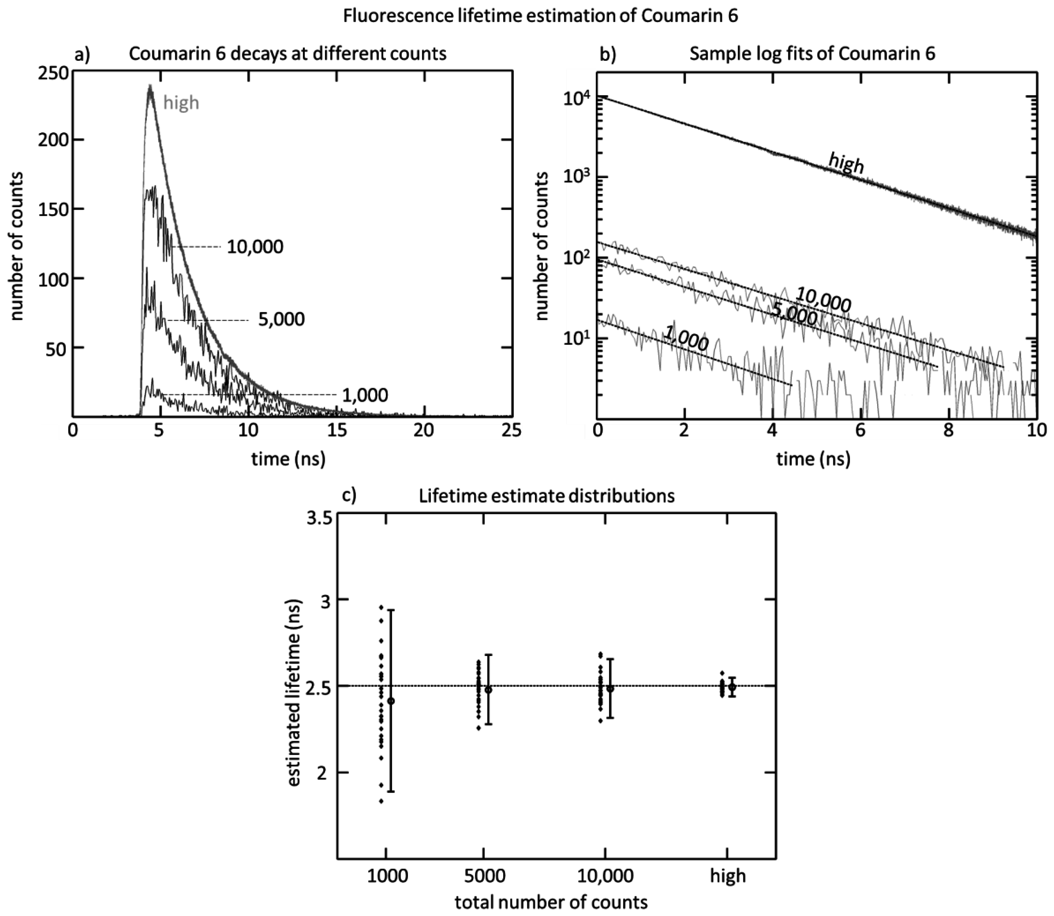
Figure 1. The SPAD array was tested by measuring the fluorescence lifetime of Coumarin 6 using a 470 nm diode laser head (PicoQuant LDH-P-C-470, Berlin, Germany). The laser was directed towards a cuvette of Coumarin 6, and the fluorescence was collected along a perpendicular path by a pair of lenses. After passing through an emission filter (Semrock FF542/27, Rochester, NY, USA), the fluorescent light was then focused onto the SPAD array, and the positioning was adjusted in order to attain a roughly uniform collection rate of 1 Mcps across the 32 detectors. The acquisition was done at a 40 MHz repetition rate, and an acquisition time designed to achieve differing total numbers of counts. Four conditions were tested: 1000 counts, 5000 counts, 10,000 counts, and a large number of counts (20,000,000), to see the impact on lifetime estimation.


 and
and 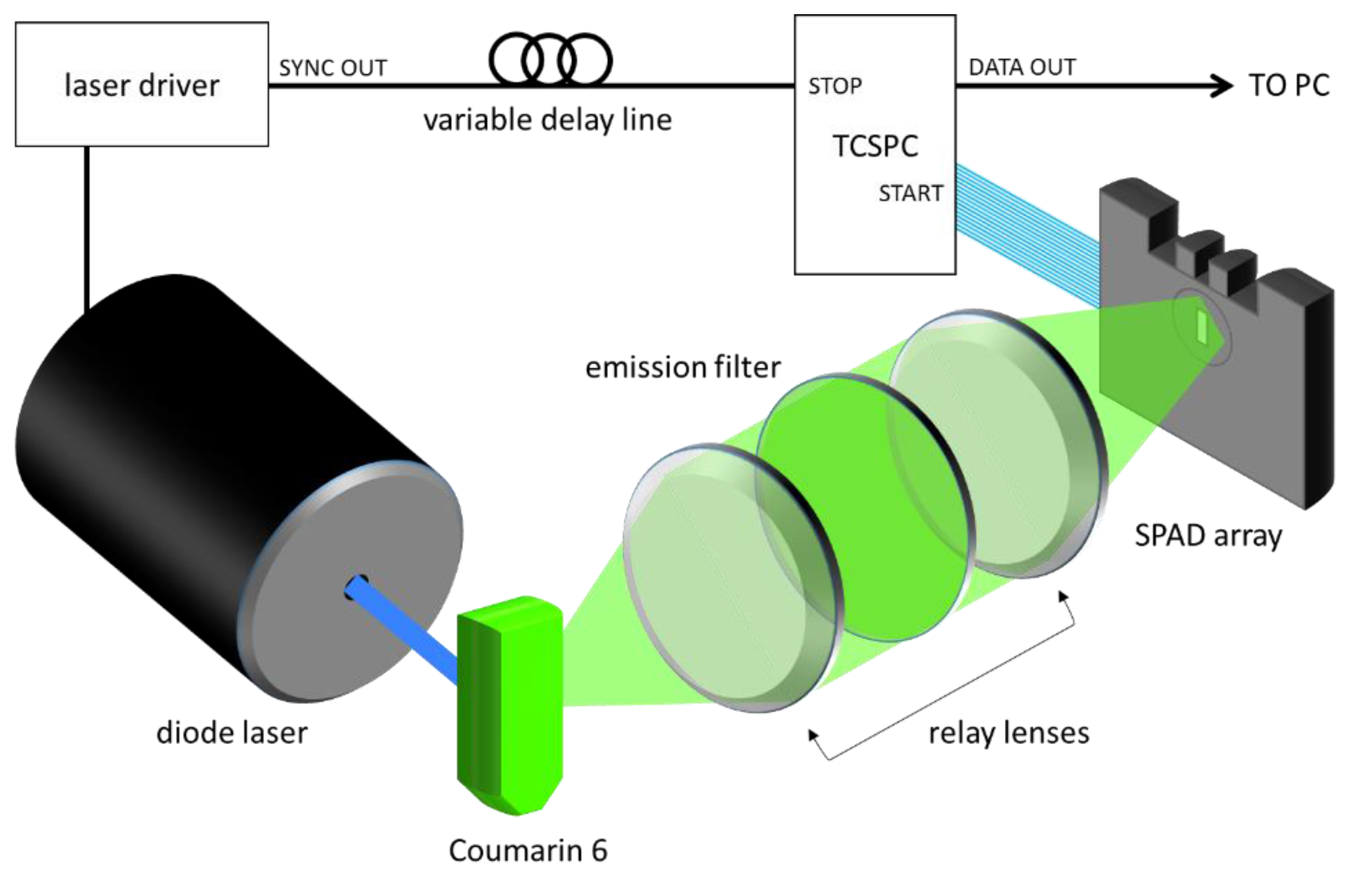

