1. Introduction
Mid-infrared (MIR) silicon photonic integration offers the opportunity to build inexpensive, compact devices or systems that address a variety of sensing and detection applications on silicon chips. Scientific, medical, industrial, and military technologies using MIR wavelengths can potentially be addressed with applications in spectroscopic analysis [
1], biological sensing [
2], environmental monitoring [
3], and astronomy [
4]. While a number of passive MIR photonic waveguides and devices have been constructed on a variety of silicon waveguide platforms [
5,
6,
7,
8], the development of integrated active components on silicon for longer wavelengths has been more limited. Thermo-optic phase shifters for the 5 µm range [
9], heterogeneously integrated InP-based type-II photodiodes for wavelengths up to 2.4 µm [
10], demultiplexers for the 2 µm range utilizing an array of similar photodiodes [
11], a fully integrated spectrometer utilizing an array of InAs
0.91Sb
0.09-based photodiodes for 3–4 µm [
12], and multiple-quantum-well InGaAs lasers which emit 2.01 µm light in continuous wave (CW) mode at room temperature [
13] have been reported.
Although InP-based diode lasers become impractical at wavelengths beyond ~2.4 µm, the quantum cascade laser (QCL) [
14] and interband cascade laser (ICL) [
15,
16] technologies provide a promising basis for integrated coherent sources extending throughout the MIR and longwave IR (LWIR) spectral bands. As a first step toward this objective, we recently reported the first successful demonstration of QCLs on silicon [
17]. These Fabry-Pérot lasers emitted at 4.8 µm when operated in pulsed mode at room temperature, with peak output powers up to 31 mW when tapers were used to transfer light from the hybrid Si/III-V active gain region into passive silicon waveguides.
Both the QCLs from [
17] and the devices discussed here were integrated on the silicon-on-nitride-on-insulator (SONOI) waveguide platform, which consists of silicon waveguides above a thin Si
3N
4 cladding, a thick SiO
2 cladding, and a silicon substrate. This SONOI waveguide can support wavelengths from 1.2 µm to 6.7 µm. Additionally, by etching off the top silicon waveguide layer, nitride-on-insulator waveguides can be constructed for propagation at 350 nm to 3.5 µm. Thus, by employing both of these options in different regions, a single silicon photonic chip can be constructed that supports all wavelengths from 350 nm to 6.7 µm.
Wavelength-selective feedback mechanisms such as gratings or loop mirrors, which we have demonstrated at shorter wavelengths [
18], may also be adapted to MIR QCLs on silicon. Distributed-feedback (DFB) lasers are attractive in many sensing applications, such as laser-based chemical bond spectroscopy, gas analysis [
19], and explosive detection [
20], which require a single frequency, narrow-linewidth source. Typically, gratings for QCLs are defined on the laser ridge sidewalls [
21], as a surface grating on the top of the laser [
22], or buried within a cladding layer [
23]. Heterogeneous integration offers the additional option of etching a shallow surface grating into the silicon waveguide underneath the III-V mesa [
24], to provide distributed feedback without the need for epitaxial regrowth. In the present work, we have demonstrated DFB QCLs integrated with SONOI waveguides on a silicon substrate, although single-mode operation has not been obtained. These lasers output over 200 mW of peak power from a hybrid Si/III-V facet, and operate to 100 °C.
2. Fabrication and Design
The integrated laser structure, SONOI waveguide platform, and fabrication process are described in [
17].
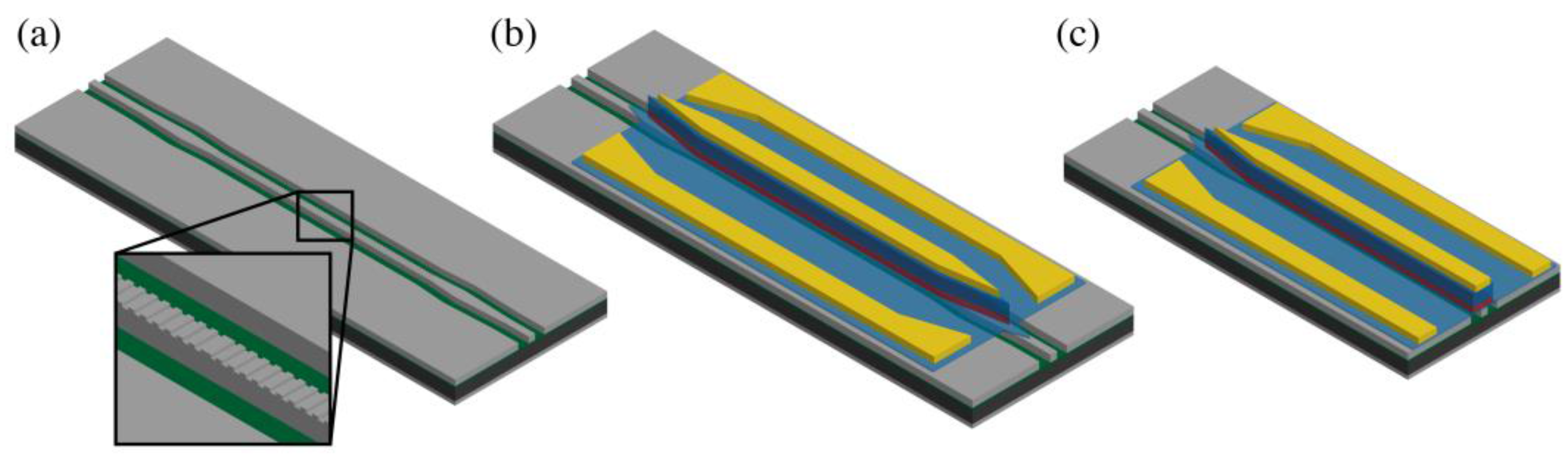
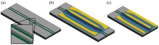
Figure 1a shows a three-dimensional (3D) illustration of the SONOI waveguide with an etched surface grating underlying the III-V layers and
Figure 1b illustrates the DFB QCL, which consists of a hybrid Si/III-V active region coupled by III-V tapers to passive silicon waveguides on both sides. End facets are formed by mechanically polishing the passive SONOI waveguides. The 3-mm-long active region is positioned on top of a quarter-wavelength-shifted shallow DFB surface grating that extends throughout the underlying silicon waveguide. The SONOI waveguide is fully etched and 1.5 µm tall.
Before the silicon waveguide is etched, the grating is patterned onto the silicon with electron beam lithography (EBL) and formed with a C4F8/SF6/Ar inductively coupled plasma (ICP) etch. The grating period employed for different devices on the chip ranges from 738 to 778 nm. Atomic force microscope (AFM) measurements of one device found a ~31% etched silicon duty cycle and 28 nm etch depth.
The silicon waveguides in the passive regions and output facets are 2 µm wide. However, the silicon waveguides expand underneath the III-V taper to aid the mode conversion. For subsequent measurements carried out to clarify the role of the tapers in the laser operation, the tapers adjacent to the output facet were removed by polishing back to immediately past the tapers. In that case, the silicon waveguide at the resulting hybrid Si/III-V output facet was slightly wider than within the rest of the hybrid active region.
Figure 1c depicts the laser structure with one taper removed.
The QCL material with 30 stages was grown by metalorganic chemical vapor deposition (MOCVD) at U. Wisconsin, Madison. The design was similar to that shown in [
25] and modified for flip-chip bonding for heterogeneous integration. In particular, a thin bottom InP contact layer and thick top InP cladding were used to increase optical confinement in the silicon waveguide while preventing overlap with the top metal.
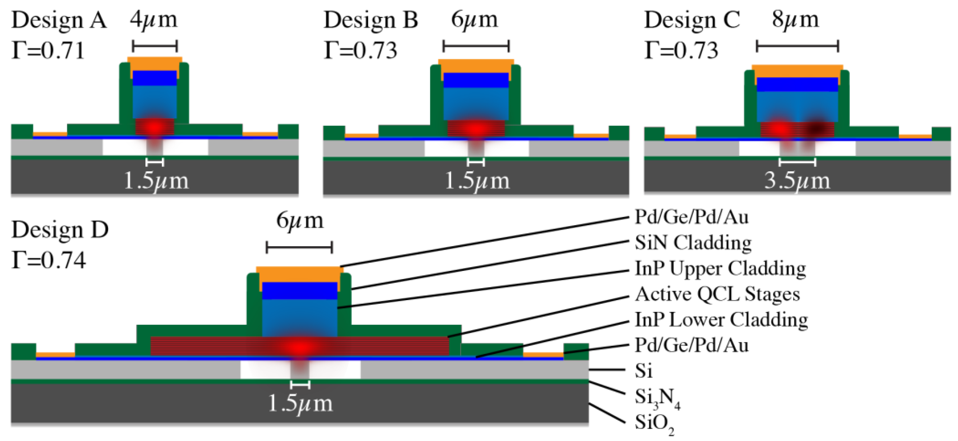
Four laser configurations with different active region waveguide geometries were tested.
Figure 2 shows active region cross-sections for the four designs labeled A–D. Designs A–C contain fully etched narrow III-V ridges as in [
17], with mesa widths of 4 µm, 6 µm and 8 µm, respectively. Design D alternatively has a 6-µm-wide upper cladding combined with a 24-µm-wide active region. The width of the silicon waveguide underneath the active region is 1.5 µm for Designs A, B, and D and 3.5 µm for Design C.
Figure 2 also overlays simulated optical modes onto the four waveguide cross-sections, along with estimated transverse optical confinement factors (Γ) in the active QCL stages. Both the active region confinement and optical overlap with the gratings etched into the underlying silicon depend on the widths of the III-V and silicon waveguides. Single-mode operation requires careful design of the laser geometry, so as to optimize both the net modal gain and the guided-mode mirror reflectivity. Fortunately, the heterogeneous silicon platform provides enhanced engineering versatility. For example, Design D, with its narrow silicon waveguide and wide active region, reduces the optical loss induced by sidewall roughness, while potentially maintaining operation in a single lateral mode. Since the current spreading below the lasing threshold is significant in QCLs, this is achieved at the expense of increasing the threshold current by the ratio of the active region width to the lateral modal extent. The far-field profiles discussed in the Results Section appear to show that, in agreement with the mode simulations illustrated in
Figure 2, Designs A, B, and D lase primarily in the TM
00 mode while Design C lases primarily in the higher-order TM
10 mode.
3. Results
The DFB QCLs were driven with 250-ns-wide pulses at a 1 kHz repetition rate. The
L-
I-V characteristics at 20 °C of each device were measured both before and after removal of the III-V tapers.
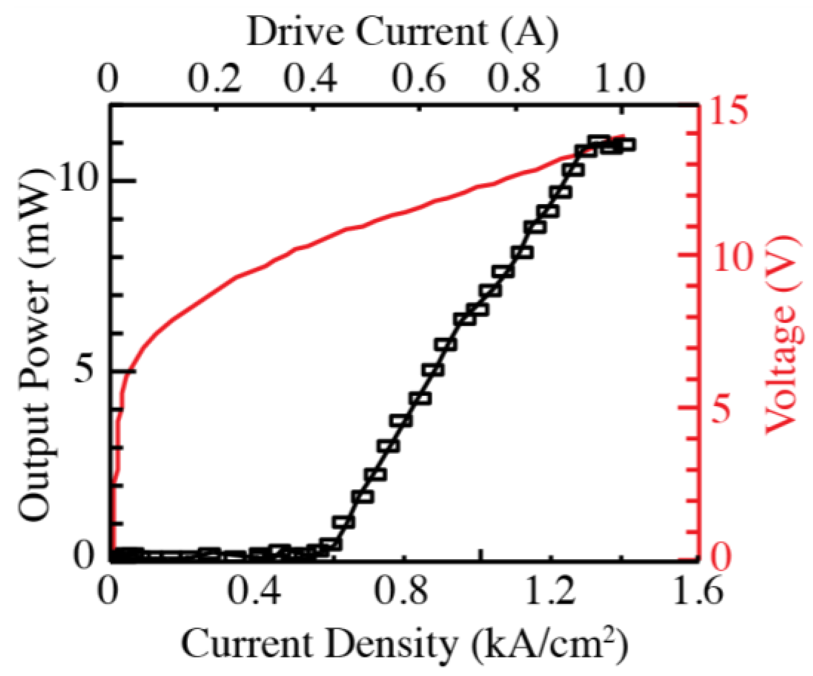
Figure 3 shows the best of the results for a device (of Design D) before the taper was removed (with the assumption that the current spreads uniformly over the 24-µm-wide active region). Although the threshold current density appears quite low (0.58 kA/cm
2), the maximum output power is only 11 mW, and the differential slope efficiency is only 23 mW/A. These observations would be inconsistent if obtained for a conventional QCL geometry with cleaved facets, since the observed low efficiency implies a high loss, which should greatly increase the threshold current density. Other devices of all four designs also displayed relatively low threshold current densities of 0.6–1.2 kA/cm
2, but even lower maximum output powers of 1.2–4.1 mW. Several of the devices (of Designs B and C) did not produce enough light to measure.
All of the lasers were re-measured following removal of the tapers from the output sides.
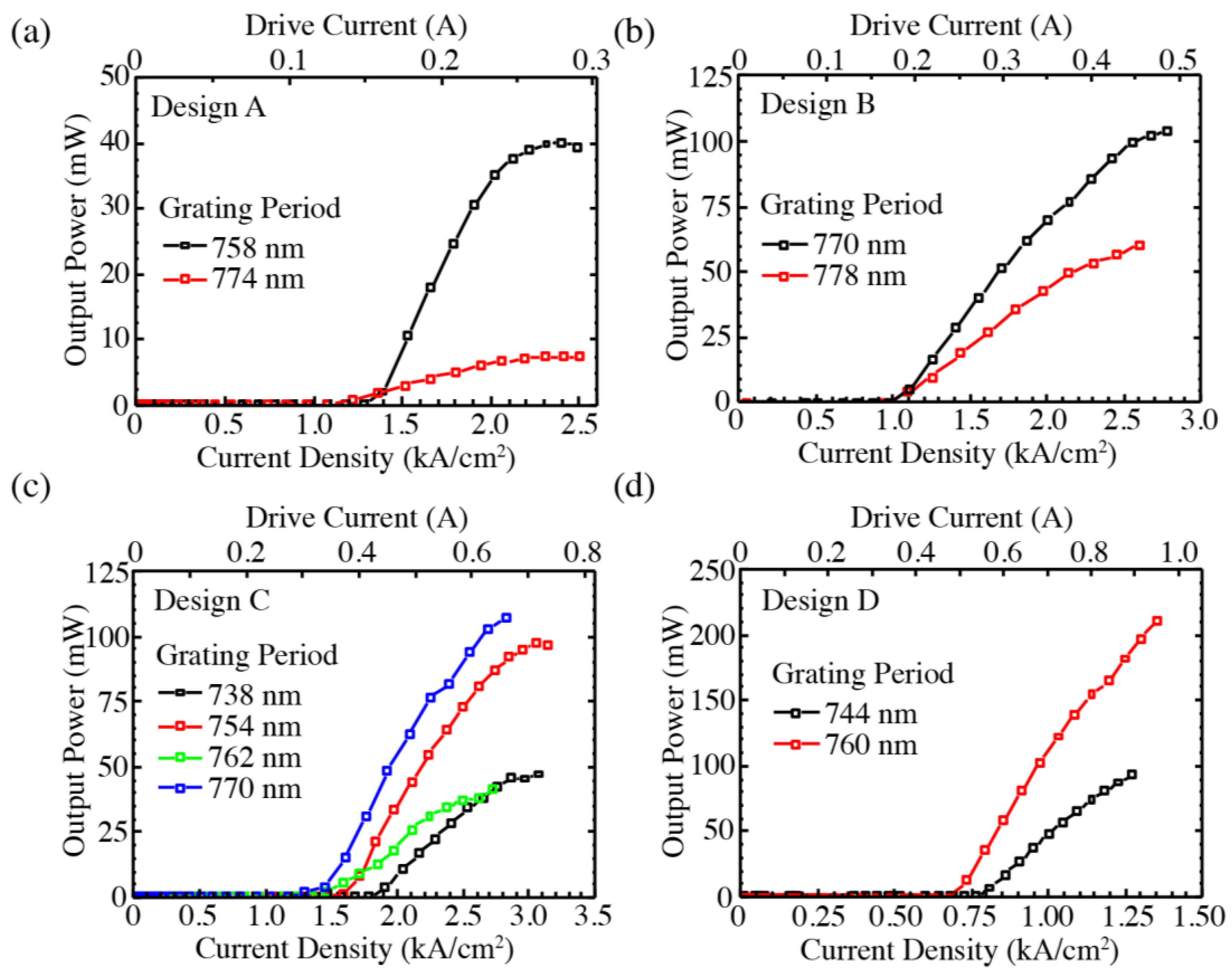
Figure 4 plots the light intensity
vs. injection current density for all of the lasers studied (two with Design A, two with Design B, four with Design C, and two with Design D). In all cases, the threshold current densities increased only slightly (by 7%–26%) while the differential efficiencies improved dramatically (by factors of 14–51). Furthermore, the devices that emitted too little light to measure when both tapers were intact became fully operational, with performance comparable to the others. Apart from one anomalous device (Design A), the slope efficiencies following removal of the tapers ranged from 161 mW/A (for a laser with Design C) to 541 mW/A (Design D). The maximum measured output power was 211 mW (not yet saturated), as seen in
Figure 4d. The threshold current densities ranged from 0.71 to 1.36 kA/cm
2 for Designs A, B, and D, while the thresholds for devices with Design C were somewhat higher (1.44–1.83 kA/cm
2).
The observation of low threshold current densities, both before and after the tapers were polished off, indicates that the taper’s primary effect was to limit the collection efficiency outside of the DFB cavity rather than to increase the loss within the primary laser cavity. The slight increase in threshold current after removal of the taper suggests that the reflectivity from the taper is higher than that of the polished (but uncoated) hybrid Si/III-V facet, whereas a large increase in the slope efficiency after the polishing indicates that the transmission through the taper is very low. This is consistent with the findings of our previous investigation of heterogeneously integrated QCLs, from which we concluded that the taper reflections are strong enough to form the primary Fabry-Pérot lasing cavity [
17].
The narrow III-V waveguide of Design A and the TM
10 mode of Design C (see
Figure 2 and
Figure 5 below) induce greater mode interaction with the InP mesa sidewalls relative to the other designs. The additional internal loss contributed by sidewall roughness most likely causes the higher current densities observed for the lasers of Design A and Design C. Although a laser with Design A displayed the second highest slope efficiency (489 mW/A), that result may be related more closely to out-coupling efficiency than to loss.
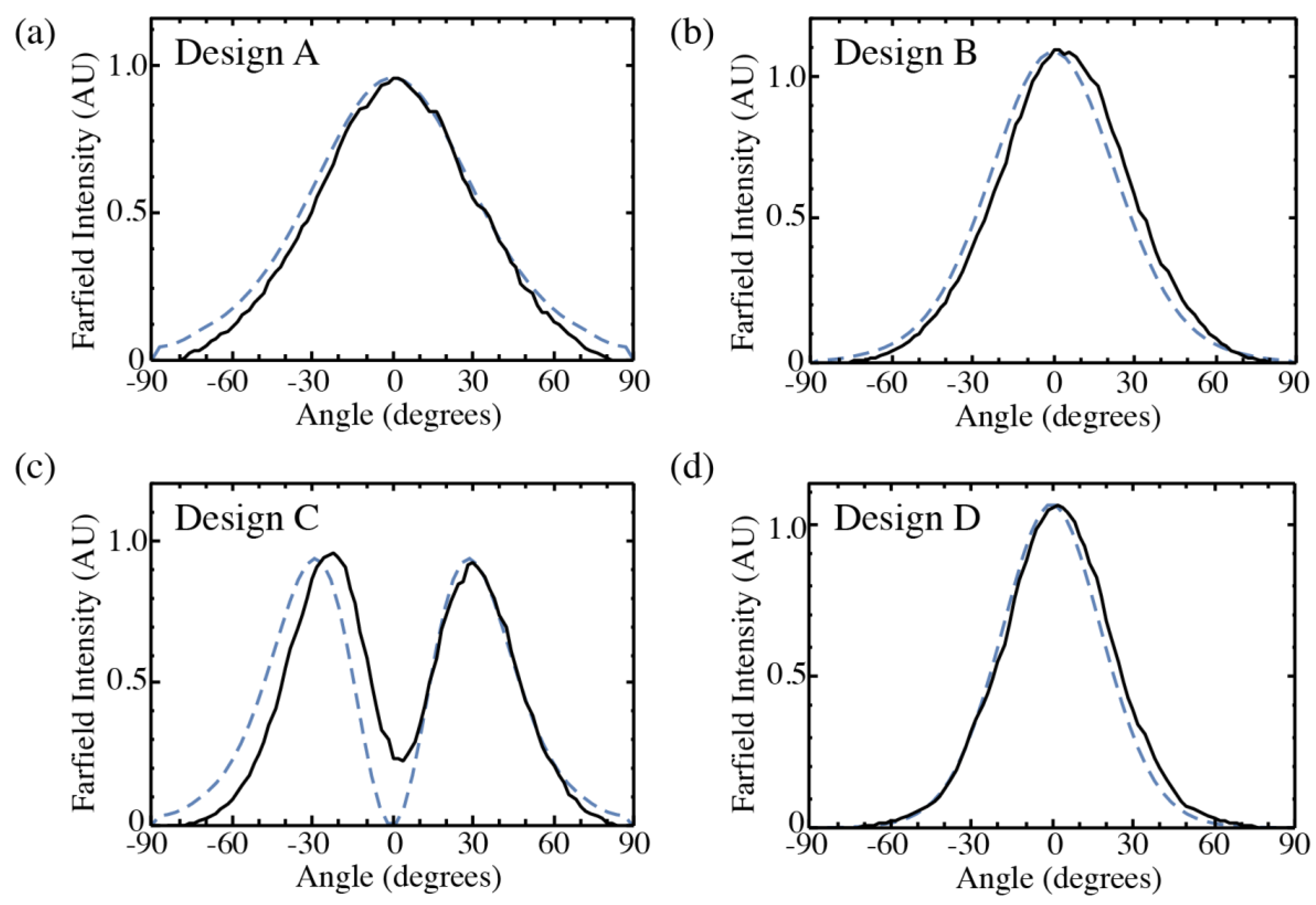
The solid lines in
Figure 5 represent the slow-axis far-field profiles for one laser with each waveguide geometry. The single-lobe distributions observed for devices with Designs A, B, and D indicate lasing primarily in the fundamental TM
00 mode. The two lobes seen in the profile for Design C indicate that the higher-order TM
10 mode dominates the emission, although the absence of a complete central null suggests that the fundamental mode also contributes. The dashed curves are FIMMWAVE simulations of the far-field distributions corresponding to the TM
00 and TM
10 modes of each waveguide design at the hybrid Si/III-V facets. These agree well with the measured profiles, with the exception of Design C near zero degrees. The fast-axis profile measured for the device with Design B displays a similar symmetric single-lobe distribution.
These mode selections are generally consistent with the optical confinement distributions simulated for each of the active cross-section designs. The second-order TM10 mode is calculated to be above cutoff for the narrow 4 µm mesa of Design A. While Design B supports a TM10 mode with high active region confinement, that mode resides almost entirely in the III-V mesa, overlaps significantly less with the Si surface grating, and interacts more with the mesa sidewalls. The 3.5-µm-wide Si waveguide of Design C is wide enough to contain much of the TM00 mode, which limits its active region confinement (Γ = 0.46) compared to the TM10 mode (Γ = 0.73). However, this configuration may allow both modes to lase simultaneously, given that the fundamental mode may suffer less from sidewall scattering loss. The apparent operation of the laser with Design D in a single mode is not as easily explained, since both the TM00 and TM10 modes have sufficient overlap with the active region and grating. One possibility is that the wider higher-order mode may have additional loss associated with optical leakage into the silicon slab on both sides of the 4-µm-wide air trenches that define the silicon waveguide.
Spectral measurements at 20 °C were acquired with a Digikrom 0.5 m monochromator with 1.5 nm resolution.
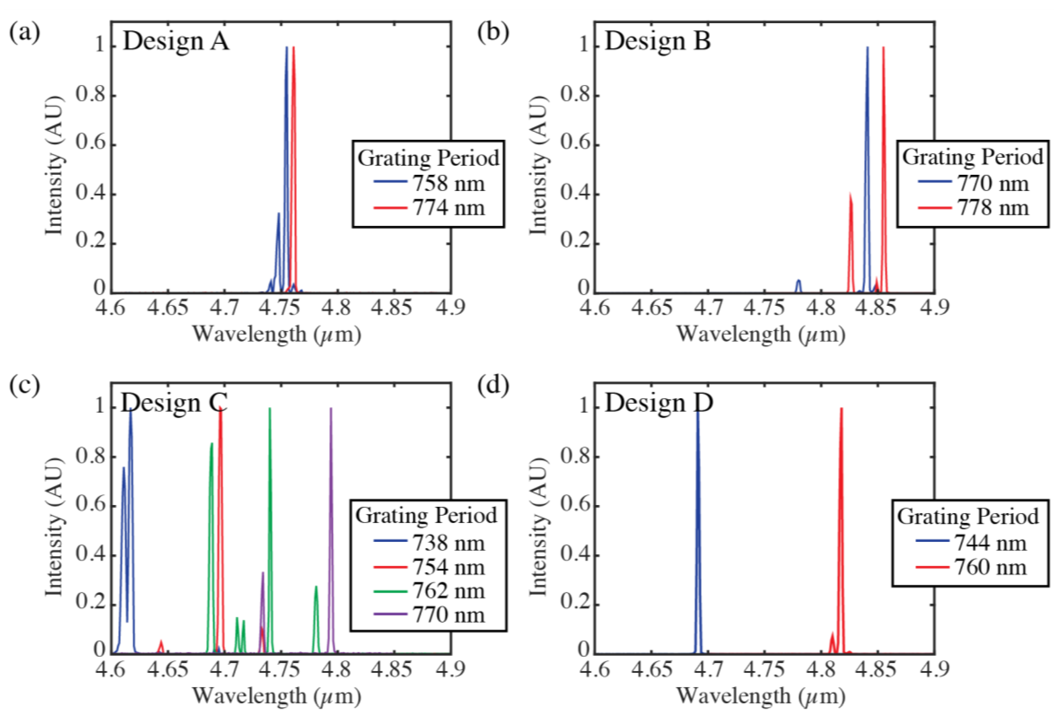
Figure 6 shows the spectra for lasers of each geometry and various grating periods. In all cases, a primary lasing peak at a wavelength ranging from 4.62 to 4.86 µm tracks the central Bragg frequency of the particular DFB grating, although many of the lasers emit in multiple modes. The weaker spectral features likely result from Fabry-Pérot resonances corresponding to reflections between the polished hybrid Si/III-V facet and the remaining III-V taper. Inconsistencies of these modes from device to device may be attributed to variations in the taper fabrication associated with non-uniform undercut at the taper tip across the chip after wet etching of the active region.
For the lasers with Designs A and D, the central mode of the λ/4-shifted DFB grating appears split by the additional cavity resonance, while the lasers with Designs B and C show evidence for higher-order grating modes at the edges of the stop-band. For all four lasers with Design C,
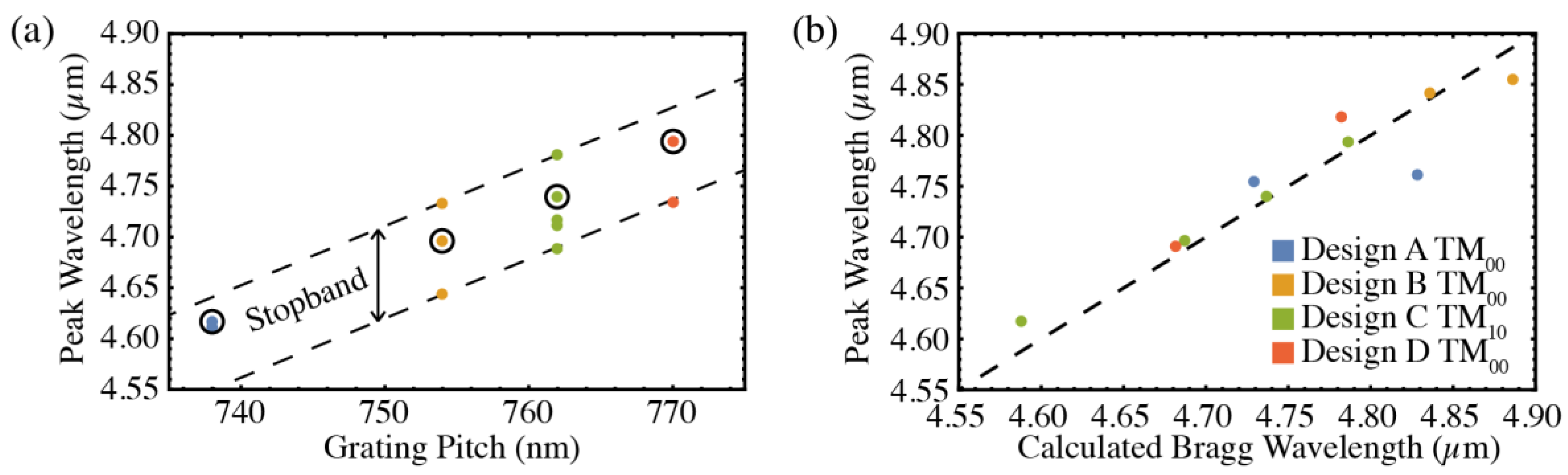
Figure 7a plots the wavelengths of the strongest peaks as a function of grating periodicity. The central peak (circled points) and two side modes follow a linear trend with the grating period, indicated by the dashed lines. This suggests a grating stopband width of 90 nm for this design.
Figure 7b shows the wavelength of the strongest peak for each laser with all four designs
vs. the estimated Bragg wavelength of the DFB grating. The first-order Bragg wavelength is calculated from the coupled mode theory approximation [
26],
, where Λ is the pitch of the grating and
is the average effective index of the mode. The average effective index is approximated by an average of the effective indices of the optical mode simulated in FIMMWAVE (TM
00 for Designs A, B, and D, and TM
10 for Design C) with and without the 28 nm grating air gap, weighted by the measured duty cycle of the grating. The Bragg wavelength calculated directly from this value of
is, on average, 1% lower than the measured peak wavelength. This inconsistency is most likely attributable to an overestimation of the effective index by the mode solver. Accordingly, the
values used to calculate the Bragg Wavelength for
Figure 7b are adjusted by a factor of 0.99. Note the nearly linear dependence of the experimental peak emission wavelength on the calculated Bragg wavelength. The only significant departure is for the same laser with Design A (emitting at ≈ 4.76 µm) that displayed anomalously low slope efficiency.
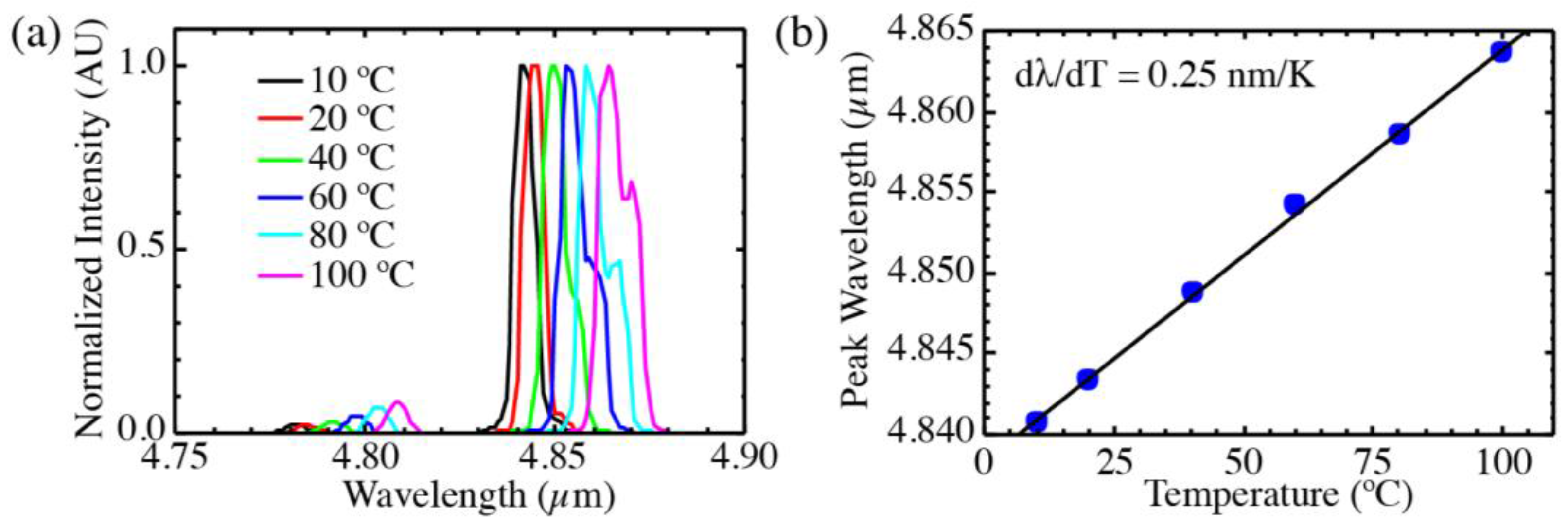
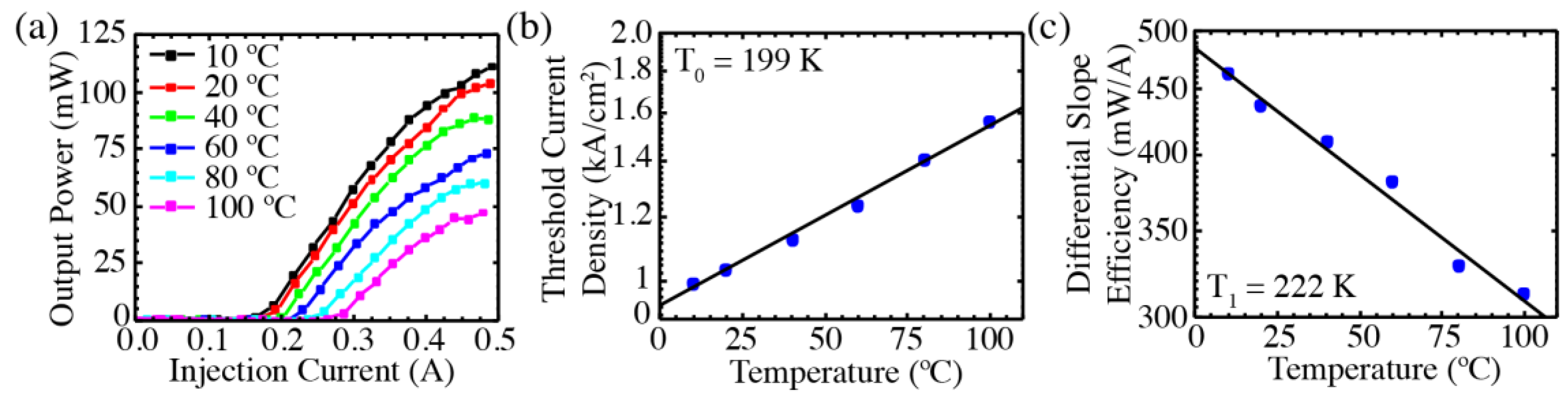
Figure 8a shows the light output
vs. injection current for the laser of Design B with a grating period of 770 nm, measured at a range of temperatures from 10 to 100 °C. The threshold current density and differential slope efficiency
vs. temperature are shown in
Figure 8b,c, respectively. The characteristic temperatures of
T0 = 199 K for threshold and
T1 = 222 K for efficiency are extracted from the exponential fits indicated by the lines.
Both of these relatively high pulsed characteristic temperatures are much higher than those observed for the Fabry-Pérot QCLs on silicon [
17], which lased in pulsed mode only to 60 °C. One possibility is that the gain peak is better matched to the Bragg wavelength at higher temperatures. The much higher
T0 and
T1 values are consistent with both the significantly lower room temperature threshold current density compared to the Fabry-Pérot devices [
17] and the relatively low injector sheet-doping density (~0.5 × 10
11 cm
−2) [
27].
Figure 9 shows the emission spectra for the same device over the same range of temperatures. The single primary peak tunes at a rate of 0.25 nm/K, which is consistent with the expected shift of the modal index that governs the DFB mode rather than the shift of the gain peak.
Given their low threshold current densities and high characteristic temperatures, CW operation of these lasers at room temperature should be achievable with improved heat dissipation.

 ,
, 

