1. Introduction
Two-dimensional (2D) photonic structures have been widely investigated in recent years, since they can be intriguingly engineered to accurately control the optical properties of passive or active devices such as optical fibers [
1], waveguides [
2] or lasers [
3,
4,
5] over a broad frequency range, from the visible to the far-infrared. The use of integrated photonic structures to tailor the behavior of light is, indeed, extremely promising for optimizing performance and for introducing advanced functionalities into photonic and optoelectronic devices.
Bi-dimensional semiconductor photonic crystal lasers usually rely on an optically pumped central area, surrounded by un-pumped absorbing regions. More recently, the same concept has been translated to the more appealing electrically pumped photonic crystal laser structures, which exploit quantum cascade laser (QCL) active regions. Laser action has been demonstrated at mid-IR [
6] and terahertz (THz) frequencies [
7] providing a fascinating solution for the achievement of simultaneous spectral and spatial (surface emission and beam shaping) mode engineering [
8,
9,
10].
In a photonic crystal QCL, operation is normally achieved on modes at the edges of photonic bandgaps [
11] or on the localized states formed by suitably designed defects [
12] within the periodic photonic lattice. This implies that efficient vertical out-coupling is typically hindered by the symmetry of the lasing modes, which usually leads to power cancellation in the far-field. This issue can be circumvented by using quasi-crystal patterns ([
13,
14]), in which the distribution of the dielectric scatterers deviates from periodicity while still being governed by a deterministic generation rule. Quasi-crystals [
15] possess optical properties lying between those of periodic photonic crystals and those of random arrangements of scatterers: on one side, they support extended band-like states with pseudo-gaps in the energy spectrum, on the other, lacking translational invariance, they also intrinsically feature a pattern of “defects” which can give rise to critically localized modes, similar to Anderson modes in random structures [
16].
Very differently from the case of photonic crystals, a band description fails in a quasi-crystal, owing to the lack of translation invariance. However, its Fourier structure S(k) [
17] can be exploited in a laser cavity to engineer the mode frequency and spacing separately, or to control the emission profile independently of the feedback conditions. S(k) indeed encodes the long-range symmetry of the quasi-crystal, providing a clear indication on the main Bragg reflection processes. These features can be exploited in a laser cavity to give rise to a rich emission spectrum, to control the frequency spacing, to increase the intra-cavity field and to simultaneously shape the far-field intensity profile.
The first reports of optically pumped quasi-crystal lasers are in the visible range [
18]. More recently, we devised the first single-mode quasi-crystal electrically pumped THz QCL [
19], exploiting a double-metal waveguide configuration and a Penrose tiling of pentagonal rotational symmetry. By manipulating
ad hoc the photon wave-vectors, the quasi-crystal resonators offer an interesting perspective for the implementation of photonic devices exploiting a large sequence of high quality factor (Q) optical modes.
Here we report on the development of seven-fold quasi-crystal QCL resonators, conceived with two different architectures: a seven-fold rotationally-invariant quasi-crystal design and a graded geometry with irregularly distributed defects. Among the broad range of conceivable seven-fold architectures, we selected two prototypical patterns providing a large sequence of high Q optical modes spanned over a ~500 GHz frequency range. Multimode emissions with up to 10 spectral lines around a central frequency of 3.1 THz have been achieved, with an average peak power of ~70 mW and beam divergence <15°.
2. Design and Simulations
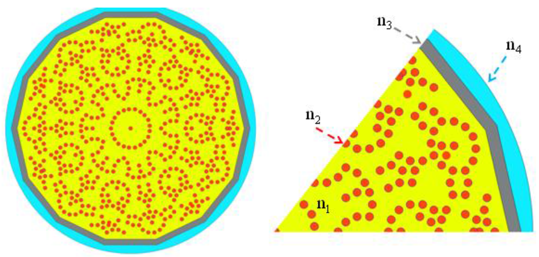
The selected QCL heterostructure was sandwiched between two metallic cladding layers to create a double-metal waveguide which confines, with an almost unitary confinement factor, the THz radiation in the direction of growth (vertical, z-axis) and allows its propagation in the x–y plane, therefore making the device a nearly ideal 2D photonic system. To implement the desired quasi-crystal geometries, holes were opened in the top metallization of a mesa structure, at the vertices of the selected tiles. Photons can be scattered there by the imprinted circular regions which exploit high-refractive-index contrast with the surrounding material, and then vertically extracted when their in-plane momentum is reduced to zero.
The exploited quasi-crystal patterns have been computer-generated with a MATLAB code, implementing the generalized dual method (GDM) [
20]. The latter algorithm allows generating quasi-crystal structures with arbitrary orientation order. In the present case, we defined a 2π/seven-rotation invariance around the center of the pattern. The code parameters have been subsequently tuned to add some localized defect points, in order to explore the effects of a high degree of disorder in the devised structures. To this aim, we explored two different geometries: a seven-fold rotationally invariant pattern (type A) and a low-symmetry seven-fold architecture with localized defect points (type B). Each pattern has been characterized via the quasi-crystal average inter-site distance
a and the radius
r of the open holes, which define the related filling factor FF =
r/a. FF has been varied here in the 23%–30% range to ensure the reasonable optical confinement needed to have high gain and sufficient extraction of light from the devices [
9,
10,
19].
The overall device surface area has been set in the range of 0.53–0.64 mm2 in order to allow a proper balance between the total dissipated electrical power and surface-related diffractive effects.
A commercial finite element (FEM) solver was used to compute the eigenvalue solutions to Maxwell’s equations for our 2D system, after assuming the structure is invariant along the z-axis and represented by an equivalent crystal composed of two materials with different local effective dielectric constants (one for the regions comprising the holes, and one for the un-patterned area).
The surrounding region is then modeled as an absorbing layer, leading to smooth boundary conditions for the guided modes. A full 3D simulation was finally performed to have access to the radiative quality factor (Qvertical) and to validate the predictions of the 2D model.
Effective dielectric constants were calculated by solving the Helmholtz equation for an infinite slab waveguide with and without top metallization, giving effective refractive indexes n
1 = 3.6 and n
2 = 2.7 in the metallized and non-metallized regions, respectively. This approximation may seem rather crude for a patterned device, as the fields are no longer uniform in the vertical direction due to the presence of the apertures [
21]. Indeed, it is known that it induces deviations in the calculation of the eigenfrequencies; nonetheless, it gives a good qualitative representation of the existing modes and their symmetries. The 2D simulations were performed after defining a surrounding domain with complex effective index n
3 = 3.6 + 0.36i, which was used to model the absorbing layer, providing smooth boundary conditions for the guided modes. Finally, an external domain having n
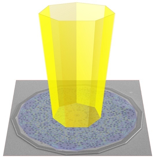
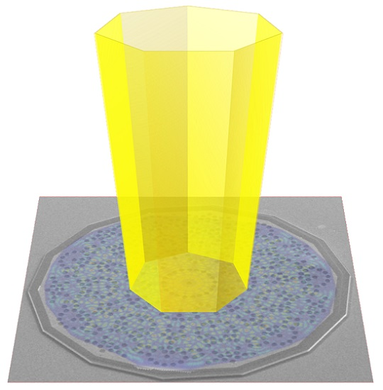
4 = 1.0 and scattering boundary conditions (SBC) was used to model the open boundaries outside the mesa. The three-dimensional (3D) model was conversely performed by considering the top and bottom metallization as perfect electric conductors (PECs). The etched GaAs/AlGaAs QCL heterostructure with the thin (7 nm) absorbing Cr border has been treated as a Cr-surrounded 10-µm-thick GaAs slab with a uniform refractive index of 4.43 + 0.31i. The thin chromium border allows suppressing any Fabry-Perot or whispering gallery mode. The SBC set over the air domain around the resonator mimic light out-coupling to the free space. A schematic diagram of the simulated device is shown in
Figure 1.
Resonating eigenfrequencies, quality factors (Q), and TM spatial profiles for the photonic modes were numerically obtained from the eigenvectors and complex eigenvalues of the FEM model.
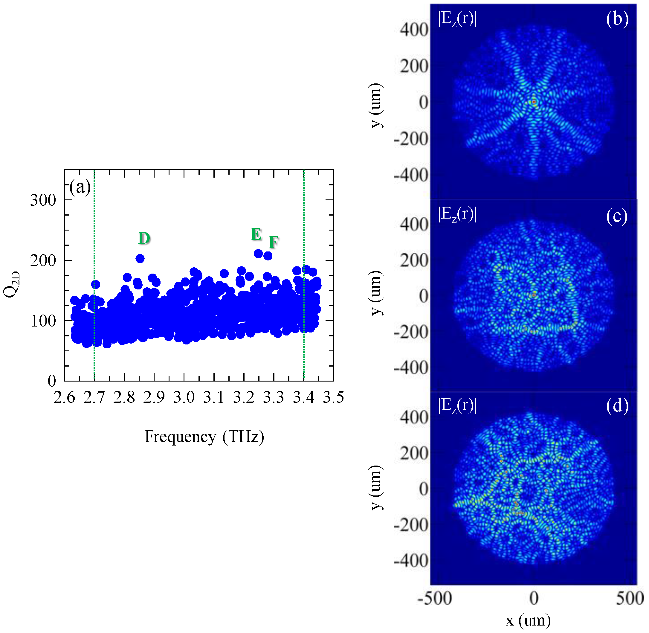
The bi-dimensional quality factor (Q2D), which accounts only for the lateral mode confinement, without including the out-of-plane radiative losses, was initially simulated to provide indication of the effects of the filling factor on the scattered light intensity. Modes with higher Q factors can here arise only from a reduced overlap with the outer absorbing boundary, i.e., from a spatial distribution mainly localized in the device center; these modes are therefore the principal ones confined by the grating feedback.
3. Results and Discussion
We therefore varied
a in the range of 29.9–32.5 µm,
r in the range of 7.1–9.2 µm while keeping FF in the range of 23%–30% for type A devices, and
a in the range of 28.5–30.0 µm,
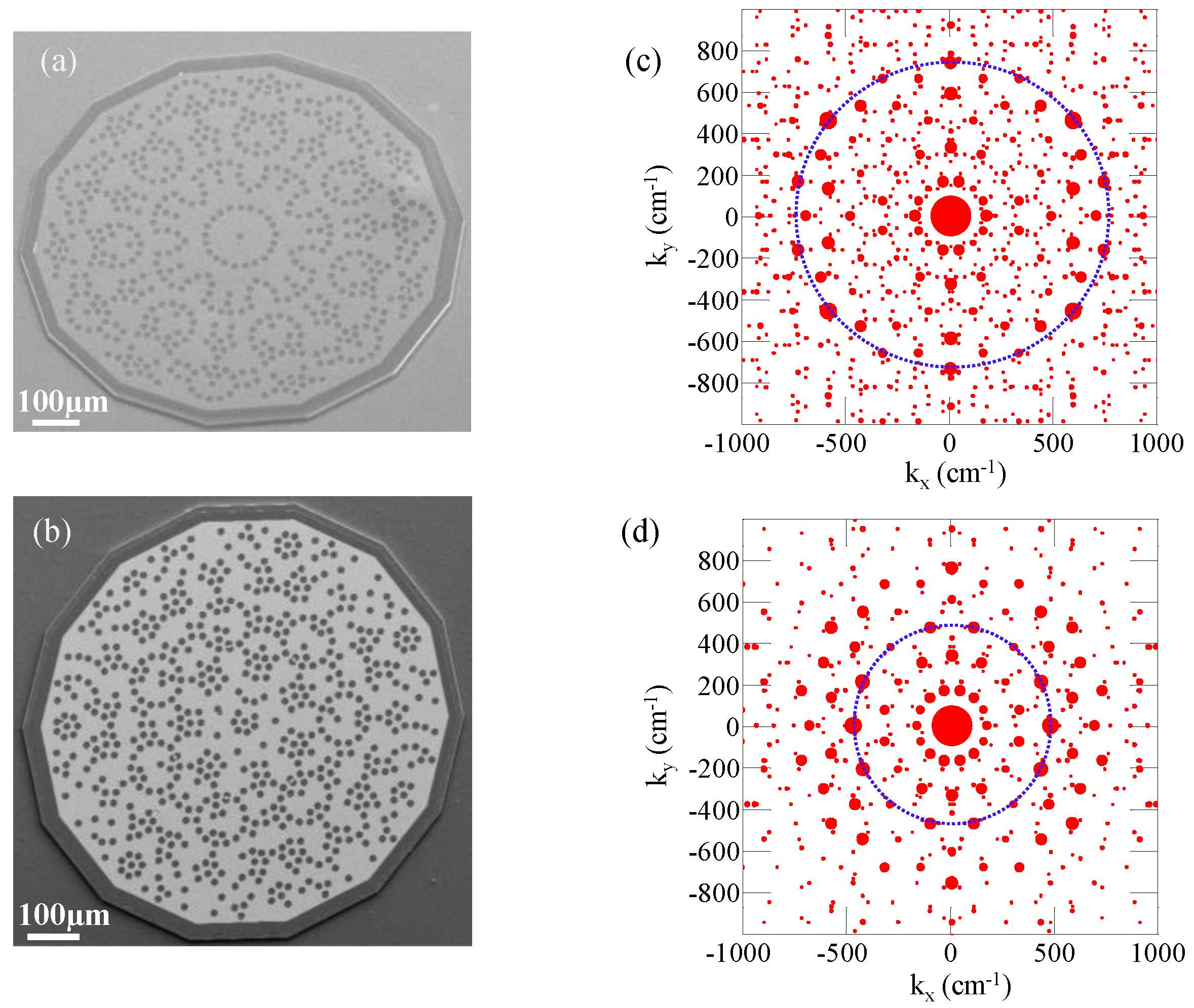
r in the range of 7.0–8.2 µm while keeping FF unchanged (23%–30%) for type B devices. The scanning electron microscope images of prototypical type A and type B resonators are shown in
Figure 2a,b, respectively, together with the related form factors (
Figure 2c,d).
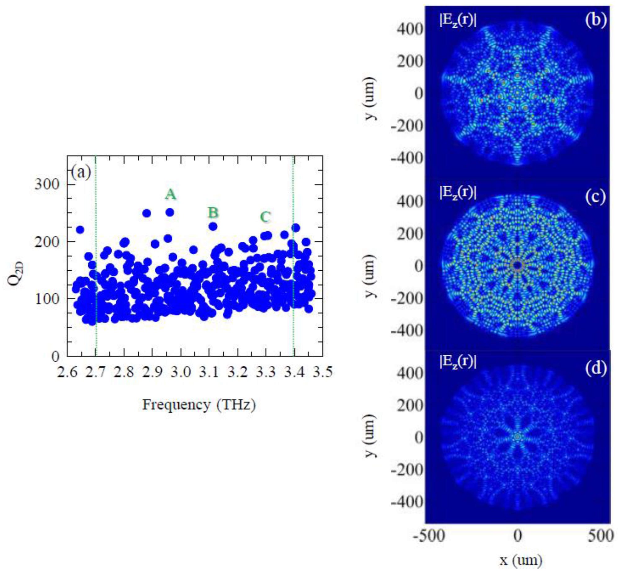
For type A devices, a large number of eigenmodes with Q
2D > 200 can be found (
Figure 2a) over a scattered background of low-Q
2D (mean value Q
2D = 125 ± 34) optical modes. Conversely, the defect quasi-crystal type B geometry shows a less scattered Q
2D frequency distribution, with maximum values in the 150–180 range (
Figure 3a). The more regular pattern architecture in the designed type A quasi-crystals induces an enhanced confinement of a few optical modes in the QCL resonator cavity, which is nicely reflected in the form factor S(k) (
Figure 2c), which shows a few sharp peaks.
Conversely, in the case of type B quasi-crystals the Fourier spectrum features more reciprocal vectors with comparable amplitude. A large number of Bragg peaks appear on concentric circles with different radii, with an angular separation of π/7. They have almost the same square Fourier coefficients, indicating they can equally contribute to the scattering mechanisms, very differently from the case of type A resonators, where a smaller number of intense reciprocal vectors is visible. Independently of the device size and the defect distribution, the geometries with intermediate FF (in the range of 24%–28%) sustain a significant number of coexisting high Q2D modes, lying in the spectral region of 2.9–3.4 THz.
The calculated 2D spatial profiles of the high Q
2D modes A,B,C and D,E,F, represented by the modulus of the electric field component in the vertical (
z) direction, are reported in
Figure 3b–d and
Figure 4b–d, respectively, and provide an initial indication of the possible Bragg peaks responsible for the feedback [
19]. Standing waves form in the crystal as a consequence of multiple diffractions on the main reciprocal lattice points, according to the relation Σ (
k −
Kj) = 0, where
Kj are reciprocal lattice Bragg points and
k is the optical mode wavevector.
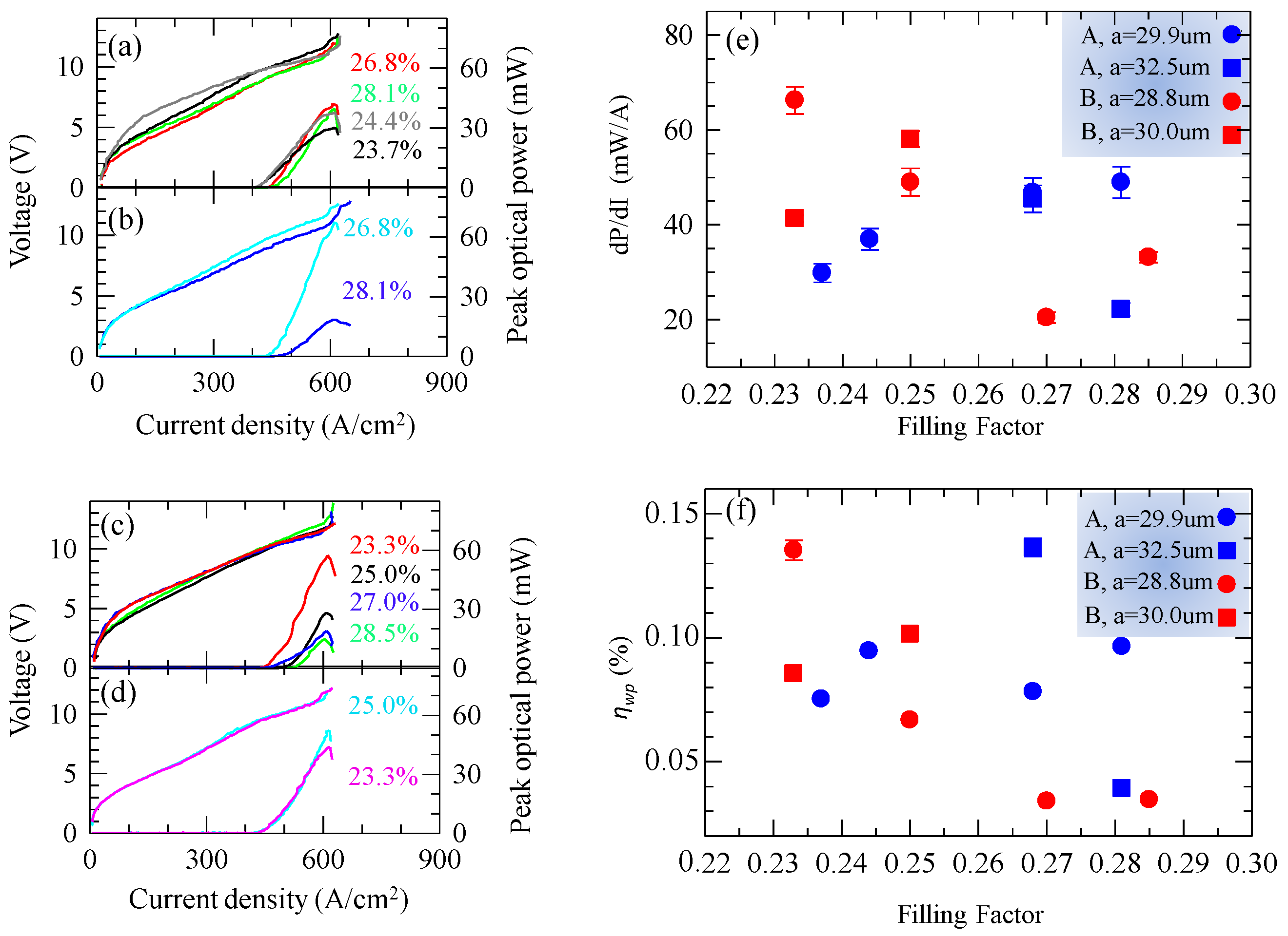
A set of resonators, for each type of architecture, was realized via a combination of optical lithography and metal deposition. The six resonators with type A geometry were engineered with the following parameters: four of them exploited a = 29.9 µm and different hole radius to get FF = 23.7%, 24.4%, 26.8% and 28.1%, respectively; two devices exploit an increased a = 32.5 µm and a radius varied to keep FF unchanged from the maximum values of the previous sample batch, i.e., FF = 26.8% and 28.1%. In the case of the defect type B quasi-crystals, the five resonators have FF = 23.3%, 25.0%, 27.0%, (with fixed a = 28.8 µm) and FF = 23.3%, 25% with a = 30.0 µm.
In order to exploit the large number of computed high Q
2D modes and achieve multicolor emissions, we selected as an active medium a hybrid bound-to-continuum QCL design combined with a single-quantum-well phonon extraction stage [
22], characterized by a 700 GHz gain bandwidth, extending from 2.7 THz to 3.4 THz.
Figure 5a,b show the measured current density-voltage (J-V) and power-current density (L-J) characteristics of the six type A quasi-crystals QCLs, collected while driving the resonators in pulsed mode at 10 K with a 1% duty cycle. The threshold current density (
Jth) strongly depends on the photonic-quasi-crystal characteristics providing an initial indication that different optical modes are active, depending on the applied boundary conditions. Specifically
Jth progressively increases at large FF and varies between 400 A/cm
2 and 450 A/cm
2. Furthermore, by increasing
a and keeping fixed FF, a further
Jth increase is induced, as shown from the comparison between panel 5a and 5b.
Figure 5c,d show the L-J-V plot of the six type B defect quasi-crystal resonators, collected under identical experimental conditions. The measured
Jth vs FF trend follows the same behavior observed in type A resonators, with slightly larger values in the range
Jth = 450–530 A/cm
2. However, differently from the previous case, a further lattice constant
a increase at fixed FF (
Figure 5d) induces a
Jth reduction.
In both sets of samples, remarkable peak optical power values were reached with a maximum of ≈ 67 mW for FF = 26.8% in a type A device and ≈ 60 mW for FF = 23.3% in a type B resonator. The vertical out-coupling is strongly affected by the implemented photonic structures, showing a clear dependence of the quasi-crystal pattern hole radius and the FF values. However, the behaviors of the type A and defect type B quasi-crystals are quite different. When the type A architecture is adopted, the peak optical power and the slope efficiency
dP/dI (
Figure 5e) progressively increase as a function of FF and then of
r when
a is kept constant at 29.9 µm, as an effect of the better vertical out-coupling in large-hole resonators. However, when both
a and
r are further increased (see comparison between
Figure 5a,b),
dP/dI shows a dramatic drop with FF, since different optical modes showing different losses and confinement factors start to become active. Conversely, in the case of the defect quasi-crystal type B resonators, the optical power progressively decreases with FF when
a = 28.8 µm, while the slope efficiency (
Figure 5e) shows a minimum around FF = 27%; by further increasing
a = 30.0 µm, the optical power and the slope efficiency start to increase again with
r, reaching ~70 mW/A as an effect of the stronger scattering strength and thus the better in-plane optical confinement.
Although the power slope efficiency is a figure of merit that relates directly to the radiative Qvert of the implementing resonators, the wall-plug efficiency (ηWP) is commonly a very practical parameter to take into account.
Usually in a symmetric photonic-crystal laser, which operates on the band-edge states of the photonic band structure, the modes can be classified as symmetric or anti-symmetric, according to the spatial symmetry of their transverse electromagnetic field components. These two classes of modes have similar cavity losses, but significantly different radiation losses. They are therefore indicated as non-radiative (antisymmetric) and radiative (symmetric) modes. Antisymmetric modes are usually weakly radiative in finite-sized resonators, with low out-coupling efficiencies. In contrast, constructive interference generally occurs for symmetric modes, leading to highly efficient out-coupling. However, non-radiative modes are typically favored for lasing, because of their lower total losses, and usually lead to very low η
WP ~ 0.01%.
Figure 5f shows the measured η
WP in our set of quasi-crystal resonators. Both type A and type B architectures allow reaching η
WP = 0.14%, which is comparable with standard double-metal Fabry-Perot resonators.
Emission spectra have been collected in rapid scan acquisition mode via Fourier transform infrared spectroscopy (FTIR) with a resolution of 0.125 cm
−1.
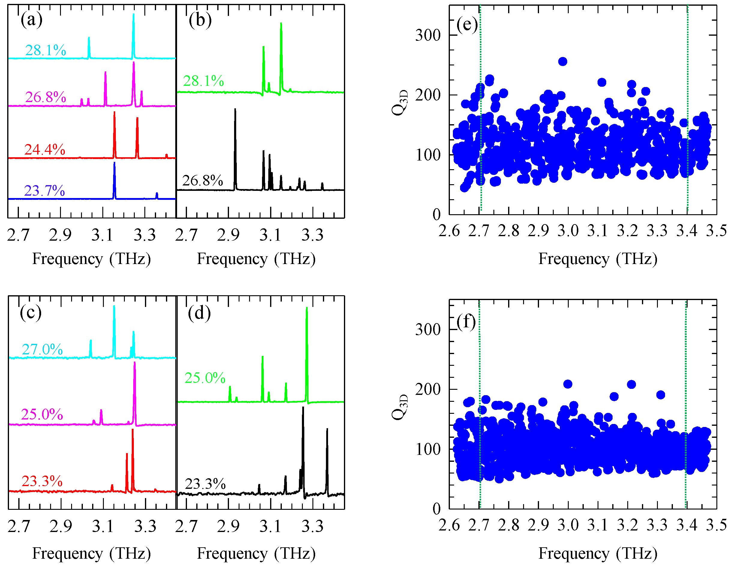
Figure 6a–d show the set of spectra collected in the type A and type B resonators, respectively, at current values corresponding to the peak optical power. Multimode emission with a maximum of 10 spectral lines spread over a 430 GHz bandwidth is achieved for type A quasi-crystals (
Figure 6b). The mode number and related intensities are highly dependent from the different geometrical parameters, resulting in an uneven amplification of the allowed modes in the photonic structures. In the case of defect mode type B quasi-crystals, the highest number of amplified modes (six) is obtained for the lowest FF = 23.3% and FF = 25% and for the larger lattice quasi-periodicity (
Figure 6d). In all cases, the frequency spacing between adjacent modes cannot be attributed to Fabry-Perot-like or whispering gallery modes, due to the absorbing boundary created by the outer chromium border.
The spectral distribution is in good agreement (with a few tens of GHz discrepancy) with the prediction of the 2D simulations (
Figure 3a,b and
Figure 4a,b) with the exception of a few modes distributed on the tails of the QCL gain bandwidth. Full 3D simulations were furthermore performed to provide a more accurate description of the modes propagating in the devised resonators, taking the radiative losses into account. The plot of the 3D quality factor (
Figure 6e,f), indicates that a few dominant high Q
3D optical modes are present, which are indeed responsible for the emitted laser lines of the corresponding resonators (
Figure 6b–d), within a <2% frequency discrepancy.
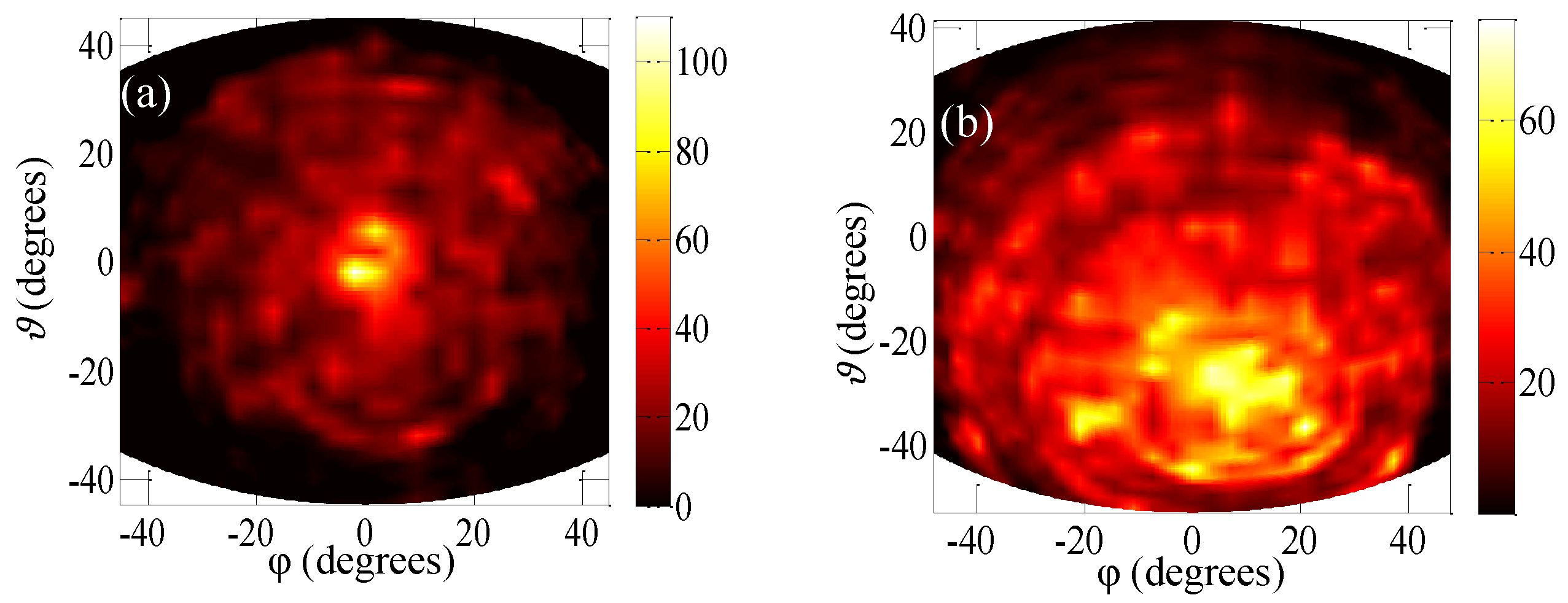
To finally investigate the optical beam emission profile of the fabricated resonators, we collected the far-field intensity distribution by scanning a pyroelectric detector in the
x–
y plane, along the surface normal direction.
Figure 7a shows the far-field intensity distribution of a type A device with FF = 26.8% and
a = 32.5 μm. The beam shape is concentrated in a 15° divergent optical spot. Conversely, the far-field intensity profile of a prototype type B laser (FF = 25.0%,
a = 30.0 μm) (
Figure 7b) is spread over a 30° divergent optical cone, reflecting the more disordered mode distribution in the resonator and the largest number of Bragg peaks which can provide feedback via a larger number of different wave-vectors.
We finally characterized the temperature performance of our quasi-crystal resonators.
Figure 8a shows the L-J-V characteristics of a type A resonator with FF = 26.8%, collected up to a maximum heat sink temperature of
TH = 105 K, which corresponds to a lattice temperature of
TL ≈ 111 K [
23].
Figure 8b reports the results of the same experiment performed on a type B quasi-crystal with FF = 25.0%, measured up to a maximum lasing temperature of T
H = 110 K (
i.e.,
TL ≈ 116 K). In all cases, the threshold current density increases with the temperature following the phenomenological formula
Jth =
J0·exp(T/T
0), which allows extracting
T0 = (113 ± 9)K for a type A laser (
Figure 8c) and
T0 = (114 ± 10)K for a type B device (
Figure 8d), demonstrating that the imprinted photonic structures do not significantly modify the device thermal behavior, which indeed matches that of the reference edge emitting double-metal QCL [
22].

