1. Introduction
In photonics and optoelectronics, many devices are based on photon absorption—e.g., photodetectors, solar cells, and so on—or are influenced in a weak or strong manner by it—e.g., optical waveguides, fibers, modulators, and so on. This very important material capability strongly depends on the semiconductor crystal type used, and it is tightly linked to the specific device component structure, as well. Indeed, its values and features change for cubic zincblende (ZB), e.g., gallium arsenide (GaAs) or indium arsenide (InAs), with respect to hexagonal wurtzite (WZ) semiconductors, e.g., binary III–nitride compounds, such as gallium nitride (GaN) or indium nitride (InN) or their ternary or quaternary alloys, such as InGaN. Moreover, the photon absorption, as all semiconductor optical properties, changes as a function of the considered structure, either the bulk or nanostructure—e.g., quantum well (QW), multi-quantum well (MQW), QW superlattice (QWSL), nanowire, single QD, multi-QD (MQD) or QDSL in nanophotonics and nano-optoelectronics.
In this paper, our interest has been focused on self-assembled QDSL and InGaN WZ materials [
1,
2,
3,
4]. A semi-analytical computational approach for QDSL minibands based on the model developed by Lazarenkova and Balandin [
5] and the interminiband absorption coefficient has been implemented in order to apply it to the InGaN semiconductor nanostructures. Compared toprevious works with a similar miniband calculation methodology [
2,
3,
4,
5,
6,
7], our method introduces, into minibands’ analysis, the strain influence on charge carriers’electric potentials and effective masses evaluated from
k∙p theory under spontaneous and piezoelectric polarizations [
1,
8], considering the minibands’ modification due to an internal electric field component along the semiconductor crystallographic polar axis (
), as well. Furthermore, we have also analyzed the miniband formation in WZ valence sub-bands, labeled as A, B and C, from that with the upper-lower energy level. Into the QDSL interminiband absorption coefficient estimation, minibands’ non-parabolicity, light polarization, as investigated in previous works for bulk [
9] and QW [
9,
10] structures, and strain influence on the interband momentum matrix element have been included. The last issue introduced into the model has been considered in a few previous works. For example, for WZ GaN and aluminum nitride (AlN), it is evaluated through density functional theory (DFT) first-principles calculations and is interpreted in the contest of
k∙p theory [
11]. Instead, here, it is derived using the
k∙p formulation for Kane parameters—
,
and
for
-conduction band (CB) charge carrier transition, where
represents one of A, B or C valence sub-bands—without strain, in which the strain-independent effective masses are replaced with those modified by strain (see
Appendix C). Furthermore, for more detailed results, an absorption coefficient component related to superlattice free excitons (see
Appendix D) is also introduced.
A superlattice was introduced for the first time in 1970 by Esaki and Tsu with a work on a 1D periodic potential for electrons formed by a series of alternate regions of different materials (dissimilar alloy compositions or unlike impurity concentrations), with a period size of several nanometers, but shorter than the electron mean free path [
12]. This structure allowed energy level minibands for charge carriers (absent in bulk structures) to be present [
13]. Minibands’ electric and optical properties can be engineered by changing the semiconductors and/or region sizes of the superlattice. Thus, this heterostructure can become useful for many applications in which specific desired energy levels or bands are needed—e.g., in full solar spectrum photovoltaic devices [
14,
15]. A one-dimensional (QW) superlattice is the most investigated and used superlattice type, due to its simpler physical-mathematical modeling and more mature fabrication technology (generally based on epitaxial growth). Indeed, photodiodes [
16], solar cells [
14,
15], LEDs [
17,
18,
19], lasers [
20] and other devices in which one or more regions—e.g., absorption region, reflector, gain active region,
etc.—are formed by a QWSL have been fabricated or investigated. On the contrary, two- or three-dimensional (2D or 3D) superlattices’ (nanowire and QD superlattices, respectively) growth technology is more complex, and the evaluation of its optical properties is generally characterized by large time and memory consumption, although a plane wave expansion is used—e.g., where each 3D charge carrier wavefunction evaluated for a given
vector of the respective 3D superlattice reciprocal space is expanded with 2197 plane waves [
21].
On the other hand, in the same years, studies on InGaN growth methods—e.g.,the electron beam plasma technique [
22] or metal-organic chemical vapor deposition (MOCVD) [
23]—led to a progressive increase of interest on this ternary alloy as a light source and absorption material. In the 1990s, the first InGaN LEDs with different emission wavelengths were demonstrated [
24,
25,
26]. With the possibility to obtain single-crystalline InN layers on sapphire (Al
2O
3) substrate by molecular beam epitaxy (MBE) [
27] and to measure its low band gap [
28], in the 2000s, investigations on InGaN absorption and the use of this semiconductor in solar cells increased [
29] for both bulk structures [
30,
31] and nanostructures [
15,
16]. Then, InGaN become a highly interesting material for high performance solar cells. Recently, researches have focused their interests on more specific InGaN features that can influence photovoltaic devices’ operation [
32,
33].
2. InGaN Semiconductor Features
InGaN is a ternary alloy semiconductor derived from the two binary III–nitride compounds, GaN and InN. It is thermodynamically stable in the hexagonal WZ crystal structure. Indium (In) content
x of the In
xGa
1-xN compound, variable from 0 (GaN) to 1 (InN), influences its mechanical, electric and optical properties. Numerical values of the parameters that describe all of these properties can be obtained with a linear interpolation (Vegard’s law) of those of GaN and InN, except for band gap
(
) and spontaneous polarization
(
) for which their own corrective bowing parameters are needed in a parabolic interpolation. The spontaneous polarization
is a polarization effect along the polar axis crystallographic direction [0001] (
i.e., the nomenclature for the WZ lattice) absent along all directions into the plane of the other two crystallographic axes (called here “in-plane”), which characterizes all WZ semiconductors. Thus, the In
xGa
1-xN band gap varies according to Equation (1) from the value for InN
= 0.78 eV to that for GaN
= 3.51 eV with the bowing parameter
= 1.4 eV. Furthermore, spontaneous polarization
can be described by an equation similar to Equation (1) in which band gaps
,
and
are replaced with
,
and
, respectively.
All physical parameter values used in this paper are taken from [
34,
35] and tabulated in
Table 1.
Table 1.
GaN and InN physical parameters taken from [
34,
35] and used in this paper. For In
xGa
1-xN, they are obtained as linear or parabolic (with theirown bowing parameter) interpolation of those of GaN and InN with respect to In content
x. The general superscript tag “
α” substitutes labels “GaN”, “InN” or “Bow” (bowing) used in the text for GaN and InN material and bowing parameters, respectively.
Table 1.
GaN and InN physical parameters taken from [34,35] and used in this paper. For InxGa1-xN, they are obtained as linear or parabolic (with theirown bowing parameter) interpolation of those of GaN and InN with respect to In content x. The general superscript tag “α” substitutes labels “GaN”, “InN” or “Bow” (bowing) used in the text for GaN and InN material and bowing parameters, respectively.
| Physical Parameters | GaN | InN | Bowing Parameters |
|---|
| Band gap () (eV) | 3.51 | 0.78 | 1.4 |
| Spontaneous polarization (C/m2) | −0.034 | −0.042 | −0.037 |
| Lattice constants (Å) | Polar axis | 5.185 | 5.703 | |
| In-plane directions | 3.189 | 3.545 |
| Energy parameters (eV) | Crystal field | 0.01 | 0.04 |
| Spin-orbit | 0.017 | 0.005 |
| Electron relative effective mass | 0.2 | 0.07 |
| Luttinger-like parameters | | −7.21 | −8.21 |
| −0.44 | −0.68 |
| 6.68 | 7.57 |
| −3.46 | −5.23 |
| −3.4 | −5.11 |
| −4.9 | −5.96 |
| Relative dielectric constant | 9.8 | 13.8 |
| Piezoelectric tensor elements (C/m2) | | 0.326 | 0.264 |
| −0.527 | −0.484 |
| 0.895 | 1.06 |
| Elastic stiffness tensor elements (GPa) | | 390 | 223 |
| 145 | 115 |
| 106 | 92 |
| 398 | 224 |
| 105 | 48 |
| |
| Deformation potential (eV) | CB | | −4.9 | −3.5 |
| −11.3 | −3.5 |
| Valence band (VB) | | −3.7 | −3.7 |
| 4.5 | 4.5 |
| 8.2 | 8.2 |
| −4.1 | −4.1 |
| −4 | −4 |
| −5.5 | −5.5 |
Moreover, In
xGa
1-xN lattice constant values
(along the polar axis) and
are a linear function of those of involved binary compounds GaN (
and
) and InN (
and
). Lattice mismatches
(along the polar axis) and
(in-plane mismatch) of the In
xGa
1-xN/In
yGa
1-yN heterostructure are evaluated as in Equation (2):
In an In
xGa
1-xN/In
yGa
1-yN heterostructure with polar c-plane growth,
i.e., along the InGaN polar axis [0001], the in-plane lattice mismatch
maximum value is 11% and is obtained for In contents
x = 0 and
y = 1 (InN growth on the GaN layer) [
36]. Mismatch during hetero-epitaxial growth induces a compressive or tensile stress, and then, the epilayer grows as a pseudomorphic layer; strained films with deformation of their own lattice and energy band structure [
34]. Stress increases with layer thickness until a mechanical relaxation process occurs. Two types of relaxation mechanisms can occur. In the former, hetero-stress is reduced with a 3D cluster formation (Stranski–Krastanov (SK) self-assembled QD growth mode) beyond a previously-grown thin pseudomorphic layer called the wetting layer. In the latter, a misfit dislocation formation relaxes the grown layer stress. While in some applications, the former can be desired, the latter induces low quality layers with a high dislocation density, particularly on hetero-interfaces [
14,
15]. Zhao
et al. [
37] and Pristovsek
et al. [
38] described theoretically and experimentally the InGaN growth with metal-organic vapor phase epitaxy (MOVPE) on a GaN buffer layer having a [0001] growth direction. Their attention was focused on In content and the growth process parameters’ influence on the critical thicknesses for two relaxation mechanisms, in order to establish what occurs in each heterostructure.
The strain effect is present in all InGaN devices that can be fabricated only as heterostructures, because unfortunately, InGaN native homogeneous substrate fabrication is today still a challenge for semiconductor growth technology. Then, an InGaN layer is grown almost always in hetero-epitaxial mode on GaN that is characterized by different lattice constants. In turn, GaN can be also grown in hetero-epitaxial mode as a buffer layer on a different substrate type with a different lattice constant, sometimes called a “foreign substrate”, such as sapphire with a 16% mismatch in crystal constant [
39], silicon (Si), silicon carbide (SiC) [
36] or GaAs [
26,
39], introducing into devices lattice mismatch stress and, consequently, mechanical strain and high dislocation defect density. Strain and, above all, dislocation defects can be reduced with some techniques based on removing the foreign substrate on which GaN was grown (sapphire substrateremoved through thelaser lift off (LLO) technique and etching by diluted hydrochloric acid (HCl) solution [
40] or GaAs removed mechanically [
26,
39]), obtaining a GaN freestanding substrate. Recently, an ammonothermal GaN growth technique has allowed the direct fabrication of a native GaN substrate, and it has been also introduced in high quality LED commercial production [
41].
GaN and InGaN are generally grown along the polar axis [0001], due to theirmature technology with respect to that of other growth directions (non-polar a-plane
, m-plane
or other planes normal to semipolar growth directions). InGaN can be grown directly also on Si, as already demonstrated in [
42]. Further, the InGaNfilms or QDs strain, as in all WZ semiconductors, induce a piezoelectric polarization, as well. Spontaneous and piezoelectric polarizations in the InGaN device regions led to a built-in electric field that modifies their operation and produces a spatial electron-hole separation with, sometimes, the consequent decrease of the absorption coefficient: the quantum confined Stark effect (QCSE) in devices based on nanostructures.
As that of its binary III–nitride compounds, for the InGaN electronic band structure at the center of the Brillouin zone (the
symmetry point in which all orthogonal components
,
and
respectively along the x, y and z directions of the reciprocal space vector
are zero), we consider only CB and the three A, B and C valence sub-bands that are involved in electronic and optical processes as optical absorption. Their doubly degenerate (two states for different charge carrier spin
(up) and
(down)) energy levels
,
and
shown in Equation (3) and their wavefunctions
,
and
in Equation (4) (VB Bloch lattice functions for semiconductor under spin-orbit and crystal field splitting) are eigenvalues and eigenvectors of the diagonalized WZ one-hole Hamiltonian matrix [
8,
43,
44,
45] without any strain effect derived by the
k∙p theory of Luttinger–Kohn:
In Equation (3),
and
are semiconductor crystal field and spin-orbit splitting energies, respectively, and
and
are defined in Equation (5). In
xGa
1-xN
and
splitting energies are functions of In content
x and derive from Vegard’s law applied on the corresponding parameters for GaN and InN semiconductors (
Table 1).
Doubly-degenerate CB energy level
and Bloch lattice functions
are shown in Equation (6) in which
is an imaginary unit.
In Equations (4) and (6)
,
,
and
are the three VB and CB Bloch lattice functions in absence of spin-orbit interaction. The former exhibit symmetry properties and a shape analogous to p atomic orbitals, the latter to s ones [
45].
3. QDSL Minibands and the Interminibands Absorption Coefficient
In this section, a model is developed in order to evaluate the minibands and absorption coefficient due to electron transitions from minibands in valence Sub-bands A, B and C to those in the CB of a generic In
xGa
1-xN/In
yGa
1-yN QDSL (with x > y), as sketched in
Figure 1.
This is a heterostructure that could be grown on a GaN buffer on a foreign substrate (see
Section 2), but in this study, the influence of the strain induced by the GaN buffer and substrate on the superlattice is neglected. This assumed condition sometimes can introduce into our results a little spectral shift with respect to the actual MQDs structure, but allows a more accurate analysis of minibands’ effect on the absorption coefficient.
We assume our samples under investigation to be in thermal equilibrium. In this condition, CB and VB quasi-Fermi level energies correspond to the unique carrier Fermi level, which is assumed as placed between the minibands of the VB and CB. This represents an ideal situation in which VB states are completely full and CB states totally empty. Moreover, the Fermi level is assumed constant throughout the whole structure. Both of these assumptions are not actual in operative conditions for a QDSL used in a device for two reasons. First of all, even in the absence of any internal or external electric field, just a very low light absorption, a process that we are analyzing in this paper, induces a splitting of electron and hole quasi-Fermi energies (the condition of quasi-equilibrium). Secondly, QDSL is generally inserted between other structures—e.g., between a region doped with acceptor impurity (p-type) and another with donor impurity (n-type) of the p-n junction—that spatially modifies the CB and VB edge with respect to the Fermi energy level. In both cases, the occupation of the charge carriers’ states will change, so reducing the light absorption. However, the QDSL absorption spectrum in thermal equilibrium gives a theoretical indication, and, e.g., its values could be used in a model for optical absorption based on minibands’ capture and emission rates [
46], which is already considered the charge carrier states’ occupation.
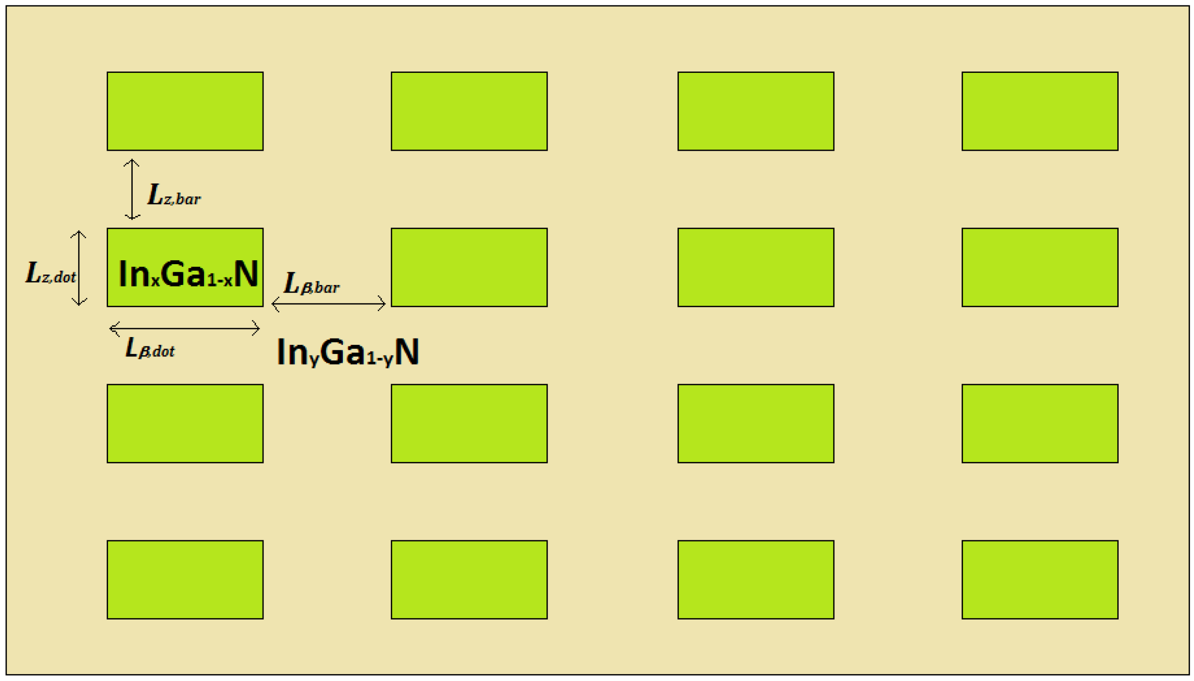
Figure 1.
InxGa1-xN/InyGa1-yN quantum dot superlattice (QDSL) 2D schematic view. Each cuboid InxGa1-xN QD (green) with sizes = = (cuboid QD with square base) and is embedded in an InyGa1-yN matrix (x > y) with inter-dot distances = =and .
Figure 1.
InxGa1-xN/InyGa1-yN quantum dot superlattice (QDSL) 2D schematic view. Each cuboid InxGa1-xN QD (green) with sizes = = (cuboid QD with square base) and is embedded in an InyGa1-yN matrix (x > y) with inter-dot distances = =and .
Another approximation used here is on QDs’ geometrical structure. Indeed, actual and most investigated self-assembled QDs’ shape is sometimes like a hexagonal pyramid [
47,
48], a truncated hexagonal pyramid [
1,
49,
50] or a lens [
51], but since minibands’ properties derive from a very large QD number, in the first approximation, it is possible to assume that QDSL miniband formation and properties are less influenced by the exact QDs shape when compared to their mean sizes and inter-distances. Indeed, our numerical investigations performed in isolated In
0.4Ga
0.6N/GaN cuboid QD with sizes 6×6×3 nm
3 reveals that the overlap value of the envelope functions is 0.77, while in [
47], for the In
0.4Ga
0.6N/GaN QD with a truncated hexagonal pyramid shape, a value of about 0.72 has been obtained. As a result, it is possible to assume that the error on the absorption coefficient values is less than almost 7% if the truncated hexagonal pyramid QDSL is approximated with cuboid QDSL. In this context, an orthorhombic symmetry and square base is assumed for the QDs’ shape (square cuboid QDs), which can simplify the superlattice modeling with the QDs’ distribution regularity in the three directions [
1,
2,
3,
4,
5,
6,
7,
18,
52]. Indeed, with these assumptions, QDSL can be considered as a semiconductor crystal with a tetragonal lattice. Furthermore, the wetting layer influence in this work has been neglected.
It is worth outlining that the procedure adopted in this work is based on a multiphysics approach,
i.e., the 3D-FEM mechanical module has been used together with the 3D-FEM piezoelectric module in order to carry out the stress distribution, and the electric field is generated by the spontaneous polarization and piezoelectric effect. Once the stress distribution and the electric field have been calculated, the energy levels in CB and in all valence sub-bands with their relative effective masses have been evaluated by applying the
k∙p theory (see
Appendix B). At this step, the QDSL miniband formation has been carried out by applying the Kronig–Penney model to 1D periodic structures obtained by decoupling the 3D problem (see
Appendix A). Moreover, the influence of built-in electric field dominant component
has been evaluated as detailed in
Appendix A. Finally, the absorption coefficient in thermal equilibrium (see
Appendix C) has been calculated by considering the non-parabolicity of minibands, the light polarization influence and the strain dependence, as well asintroducing the absorption coefficient component related to free excitons of the superlattice (see
Appendix D). The procedure sequence is shown in the following flow chart (
Scheme 1).
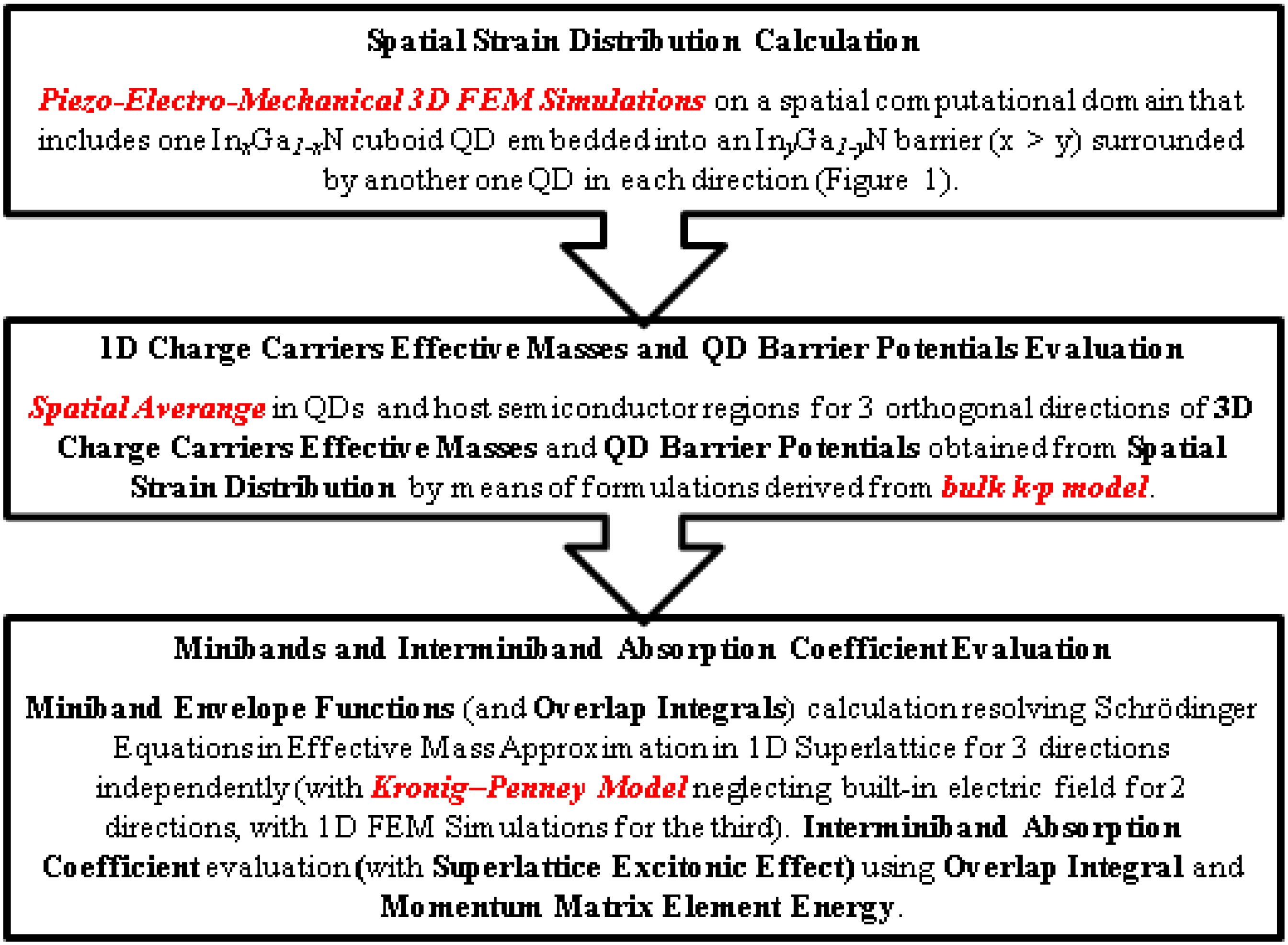
Scheme 1.
Developed procedure sequencefor InGaN cuboid QDSL interminiband absorption coefficient evaluation.
Scheme 1.
Developed procedure sequencefor InGaN cuboid QDSL interminiband absorption coefficient evaluation.
4. Simulations, Results and Discussion
First of all, in this section, our developed model has been applied to investigate an In0.4Ga0.6N/GaN cuboid QDSL. In such a structure, dots and barrier regions band gaps are equal to 2.08 eV and 3.51 eV, respectively, while neglecting strain, spontaneous and piezoelectric polarizations. This structure will be characterized by CB (VB) miniband formation with energy levels between those of semiconductor CB (VB) edges in QDs and barrier regions.
Then, it is possible to predict spectrum values for the interminiband transition absorption coefficient included into 2.08–3.51 eV (a light wavelength of 353–596 nm). We assume dot base width
= 4–6 nm, dot height
= 3 nm and inter-dot distances
= 5 nm and
= 2.5 nm. In
Figure 2, we show the strain distribution of the dominant x component as evaluated by FEM simulations (see
Appendix B).
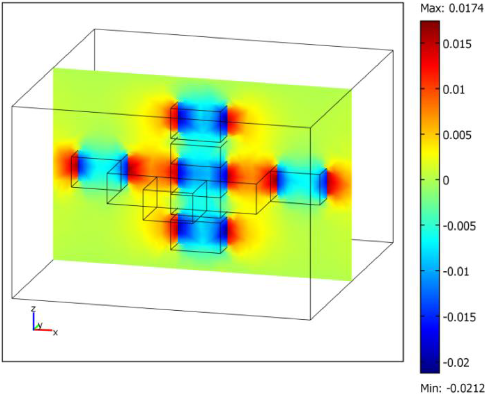
Figure 2.
In0.4Ga0.6N/GaN QDs’ dominant x strain component distribution for dot sizes = 5 nm and = 3 nm and inter-dot distances of = 5 nm and = 2.5 nm.
Figure 2.
In0.4Ga0.6N/GaN QDs’ dominant x strain component distribution for dot sizes = 5 nm and = 3 nm and inter-dot distances of = 5 nm and = 2.5 nm.
After FEM 3D piezo-electro-mechanical simulations and application of the 1D Kronig–Penney model for each direction, barrier potentials for charge carriers in QDs and allowed energy minibands are found as indicated in
Table 2.
Table 2.
In0.4Ga0.6N/GaN QDSL electronic features for = 3 nm, = 5 nm, = 2.5 nm and = 4–6 nm without miniband splitting due to the built-in electric field.
Table 2.
In0.4Ga0.6N/GaN QDSL electronic features for = 3 nm, = 5 nm, = 2.5 nm and = 4–6 nm without miniband splitting due to the built-in electric field.
| (nm) | Electronic Features | Electrons | A Holes | B Holes | C Holes |
|---|
| 4 | 1D QD barrier potential (eV) | | 0.985 | 0.169 | 0.15 | 0.14 |
| 1.07 | 0.124 | 0.13 | 0.211 |
| 3D allowed minibands | 111, 112, 211 (121), 221 | 111 | 111, 112 | 111, 211 (121) |
| 5 | 1D QD barrier potential (eV) | | 0.986 | 0.167 | 0.146 | 0.148 |
| 1.081 | 0.117 | 0.126 | 0.224 |
| 3D allowed minibands | 111, 112, 211 (121), 221, 212 (122), 311 (131) | 111 | 111, 112, 211 (121) | 111, 211 (121) |
| 6 | 1D QD barrier potential (eV) | | 0.983 | 0.166 | 0.142 | 0.152 |
| 1.082 | 0.113 | 0.124 | 0.23 |
| 3D allowed minibands | 111, 211 (121), 212 (122), 311 (131), 112, 221, 321 (231), 411 (141), 222 | 111, 112 | 111, 211 (121), 112, 221 | 111, 211 (121), 311 (131), 221 |
As shown in
Table 2, an increase of dots’ width generally reduces the QD barrier potential for charge carriers in CB and A and B valence sub-bands, while for those in C valence sub-bands, there is an opposite effect due to the strain, as can be seen from Equation (B5). This particular effect, as verified from FEM 3D piezo-electro-mechanical simulations, is the result of two contrary strain contributions in QDs and barrier regions. Indeed, while into larger dots, compressive strain and consequently an increase of the potential edge arereduced, tensile strain in barriers is applied to a more extended region, so increasing its total effect and lowering the barrier edge energy level. Between these two effects, those in barrier regions are dominant and reduce the QD barrier potential. On the other hand, this effect does not lead to a reduction of the numbers of minibands, because it is above all related to barrier regions’ relative dimensions with respect to those of dots for each direction. Then, for smaller inter-dot distances with respect to dot sizes, there is a tendency to have more minibands, e.g., an increase of the number of 3D minibands can be obtained with increasing the dot size, without changing that of barriers.
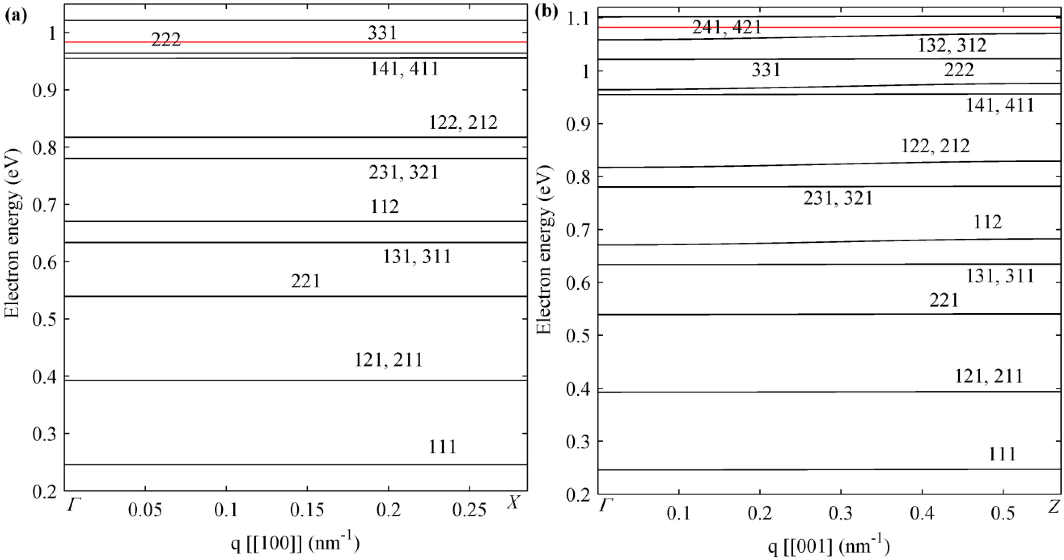
In
Figure 3, electron miniband dispersion in
-space for the third structure of
Table 2 is shown along the two representative [[100]] (
Figure 3a) and [[001]] (
Figure 3b) directions (here, a double square bracket for differently labeling superlattice reciprocal space directions is used with respect to the single-square bracket for the directions of the crystal reciprocal space). Fourteen very thin minibands—energy widths with values around that of 1–12 meV—stay under the barrier continuum energy edge (red line) of both directions. Five couples of these minibands are degenerated in the
point and are symmetric over the plane in the
-
direction in the 3D reciprocal space. This is due to the tetragonal crystal structure of the square cuboid QDSLs analyzed. One of each couple of these minibands is indicated with round brackets in
Table 2.
In the results shown in
Figure 3, in order to evidence the features of the miniband formation, we have considered the influences of the built-in electric field in the stress distribution and then in the average values for the barrier potential and effective masses evaluated (direct influence in Equations (B1)–(B5) and indirect in Equations (B7)–(B8) of
Appendix B), neglecting the direct and strong change of the Schrödinger equation (Equation (A1) of
Appendix A) and charge carriers’ steady states that correspond to neglecting the energy band bending typically present in WZ materials. For the nanostructures under investigation in this work, the value of the z-component
obtained from 3D FEM simulations is dominant with respect to
and
. For this reason and for a more accurate analysis of this effect, we consider the electric field only along the polar axis. Furthermore, the values of electric field
along the central axis of cuboid QD in the z direction obtained are different for dot and barrier regions, but almost constant. For example, from FEM simulation in the second sample of
Table 2, two different values of the built-in electric field,
= 0.99 MV/cm and
= −1.02 MV/cm, are achieved. Since QDs’ semiconductor lattice constant is larger than that in the barrier regions, a compressive stress in QDs and a tensile one inbarriers is induced in QDSL (
Figure 2) with a consequently opposite sign for
and
along the z direction. Moreover, in the numerical evaluations of
and
, the spontaneous polarization provides a very low contribution with respect to the piezoelectricity.
Figure 3.
In0.4Ga0.6N/GaN QDSL electron minibands for dot sizes = 6 nm and = 3 nm and inter-dot distances of = 5 nm and = 2.5 nm along the (a) [[100]] and (b) [[001]] directions in reciprocal -space. The red line represents the electron energy potential in the barriers‘ region.
Figure 3.
In0.4Ga0.6N/GaN QDSL electron minibands for dot sizes = 6 nm and = 3 nm and inter-dot distances of = 5 nm and = 2.5 nm along the (a) [[100]] and (b) [[001]] directions in reciprocal -space. The red line represents the electron energy potential in the barriers‘ region.
However, these values are too large to be considered negligible in the 1D Schrödinger equation along the z direction. Indeed, 1D minibands along the InGaN polar axis [0001] (
Figure 3b) are split in a series of Wannier–Stark levels with envelope functions localized in a few dots, if the terms for
and
are included in the 1D Schrödinger equation.
It is worth outlining that in the FEM simulations of Wannier–Stark levels, we have assumed fifteen periods in the z direction. This number of periods has been proven to be a good trade-off between the smaller computational domain and the solution accuracy. Indeed, our preventive investigations reveal that envelope functions
tend to be localized in a number of 1D superlattice periods increasing with
. In addition, numerical analysis obtained forcing the built-in electric field to zero reveals that in the samples analyzed, a few (
= 4) 1D minibands in the z direction are generally allowed. As a result, we can conclude that fifteen periods are enough to describe the spatial distribution of the wavefunction
accurately. It is interesting to note that, sometimes, the number of QDs in which the envelope function
is localized is the same as the order number
, depending on the energy distance between consecutive Wannier–Stark levels
given as:
In particular, the abovementioned condition takes place for structures in which
is larger than the QDs energy barrier
as occurs for charge carriers in valence sub-bands in our samples. In
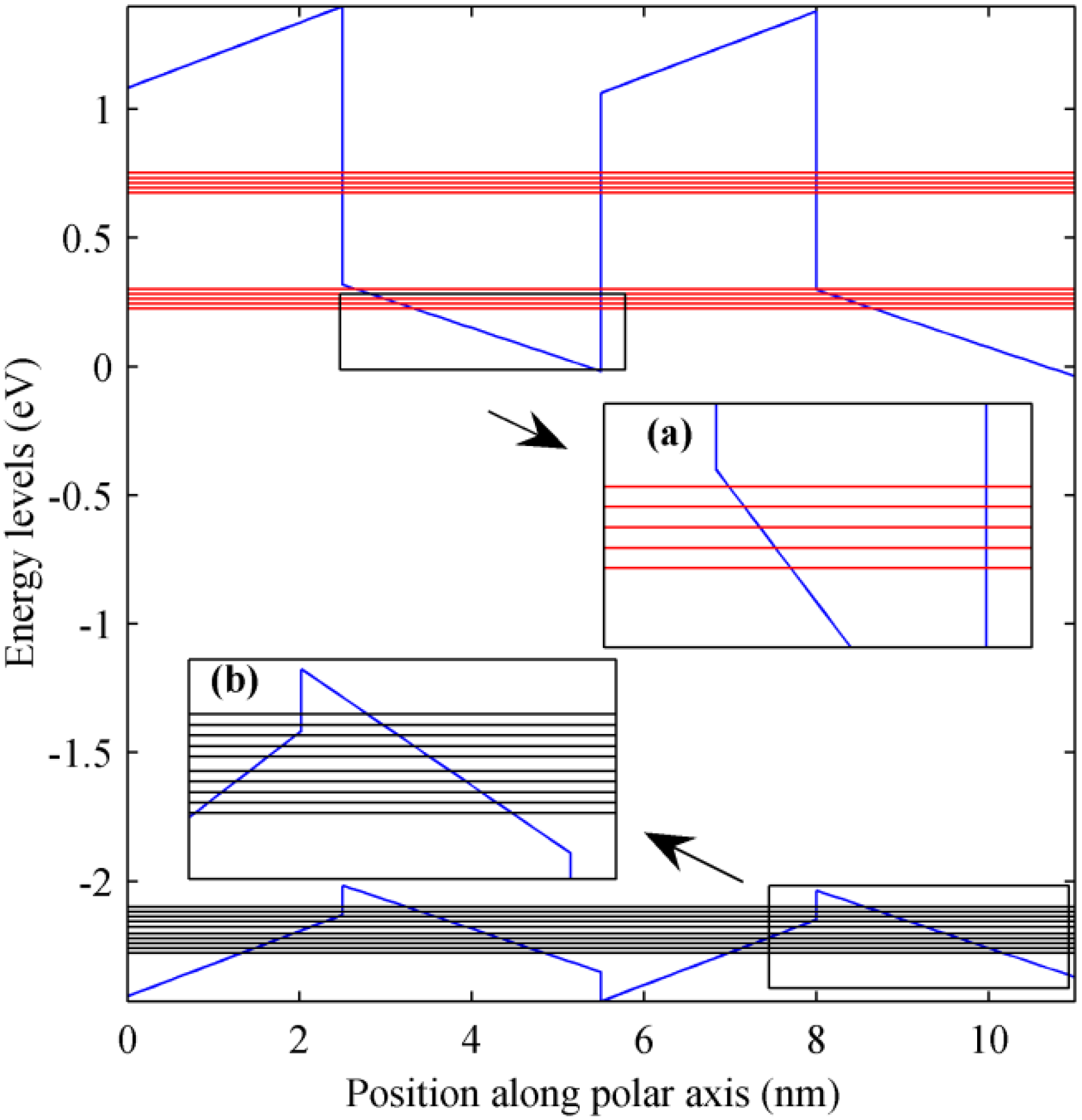
Figure 4 energy levels for charge carriers in CB and in the A valence sub-band are shown. For both charge carriers, two types of envelope functions and then two groups of Wannier–Stark levels occur with an energy distance between consecutive allowed levels
= 19.2 meV. Although bands’ edge bending in an ideal infinite superlattice leads to an infinite number of Wannier–Stark levels for each
throughout the whole structure, in our 1D FEM simulation, we focus the investigation on Wannier–Stark levels related to localized envelope functions that are not negligible in one dot in the middle of the 1D FEM simulation domain. Then, five levels for each group are considered, and from the corresponding evaluation of the absorption coefficient, the information for the infinite structure can be extrapolated. In the sample of
Figure 4, the groups of five energy levels for CB are separated, while for the A valence sub-band, they overlap. Often, nanostructures can be characterized by anisotropy, whichmodifies their responses to an external input as a function of its application direction. For the optical absorption, it is possible to estimate its dependence on light polarization. Our developed absorption coefficient model based on a Fermi’s golden rule implementation done by using a numerical integration over the first Brillouin zone allows analysis of the light-matter interaction for different directions of
in order to have a more accurate investigation of light polarization influence.
Figure 4.
Wannier–Stark ladder energy levels (red lines for charge carriers in CB and black lines in the A valence sub-band) along the polar axis direction in an In0.4Ga0.6N/GaN QDSL with dot sizes = 6 nm, = 3 nm and inter-dot distances = 5 nm and = 2.5 nm. The subplot insets are the enlargement for (a) CB and (b) the A valence sub-band. Arbitrarily, an energy value of 0 eV has been assigned to the minimum of the CB edge into the dot in the first period shown.
Due to the different nature of A, B and C valence sub-band Bloch lattice functions, we have divided this analysis into two parts. At the first step, we have analyzed the influence on carriers’ transition valence sub-band from A to CB minibands (
Figure 5). Indeed, the A valence sub-band Bloch lattice functions, like heavy holes of ZB semiconductors, are characterized by only two directional
and
components, as is possible to see from Equation (4). On the contrary, B and C valence sub-bands’ Bloch lattice functions present a directionality given by all three
,
and
components. Furthermore, they are in a reciprocal relationship through the
and
parameters defined in Equation (5), depending on the In content of InGaN.
In
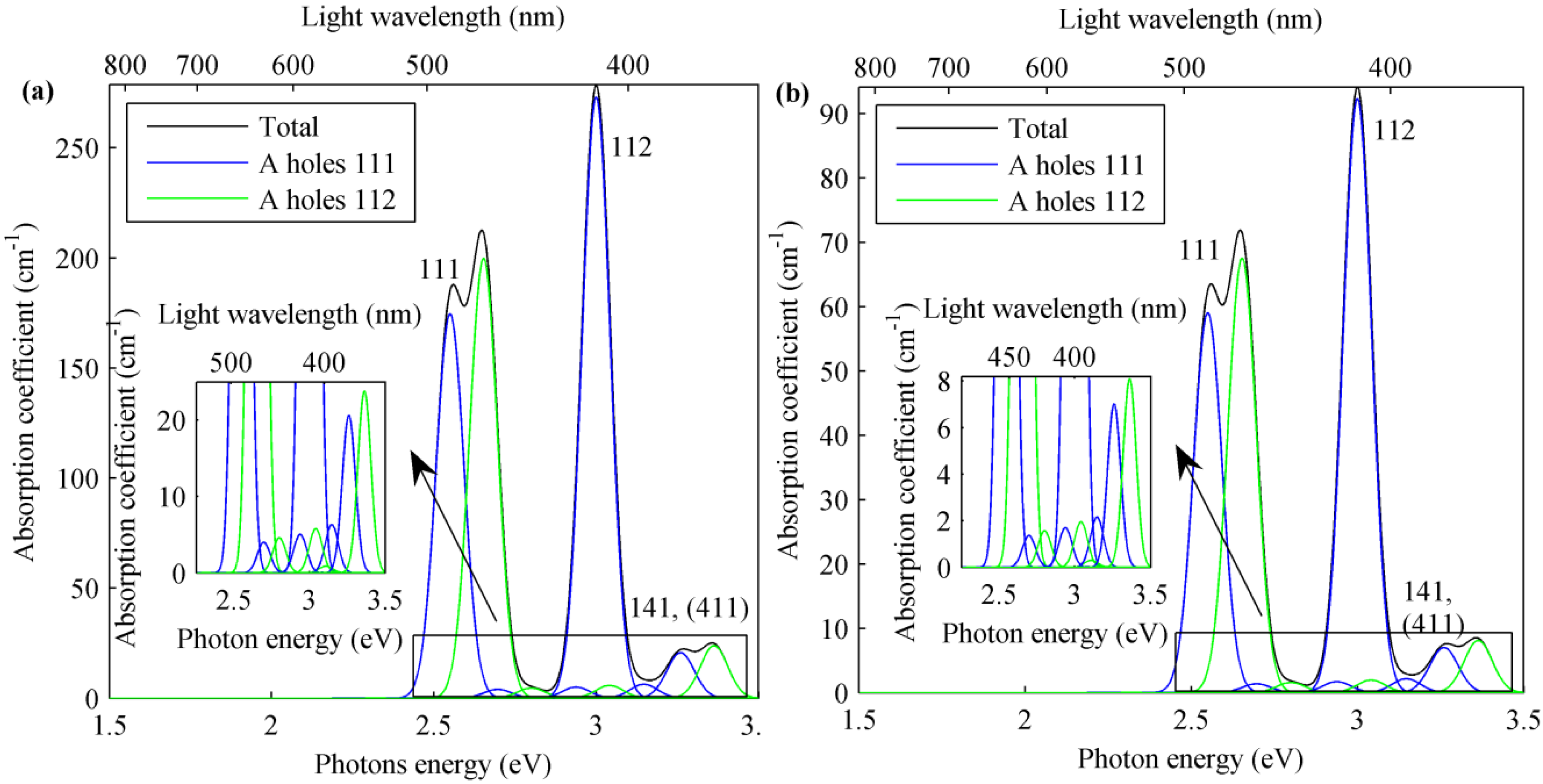
Figure 5, the absorption coefficients are shown as evaluated for the third sample in
Table 2 for interminiband transitions from the A valence sub-band to CB minibands for (a) TE- and (b) TM-polarized incident light. The absorption coefficient profile in the two cases is similar, but values for TE-polarized light are almost three-times larger than for TM-polarized light. Generally, this is due to the InGaN anisotropy properties as a WZ semiconductor, but it is also influenced by strain, QD shape and In content in the structure. The highest peaks are obtained for transitions between the first minibands in the VB and CB. The maximum value of 273 cm
−1 occurs for interminiband transition from the 111 A valence sub-band to 112 CB for a photon energy of 3 eV (wavelength of 413 nm). The other higher peaks are related to interminiband transitions from 111 and 112 A valence sub-bands to 111 and 141 (with 411) CB minibands.
Table 3 shows all interminiband absorption coefficient maximum peaks for the three QDSL structures described above and presented in
Table 2.
Figure 5.
Absorption coefficient for interminiband transition from A valence sub-band to CB minibands for (a) TE- and (b) TM-polarized light in In0.4Ga0.6N/GaN QDSL with dot sizes = 6 nm, = 3 nm and inter-dot distances = 5 nm and = 2.5 nm. Integer numbers near the highest peaks specify the CB miniband involved in the absorption process.
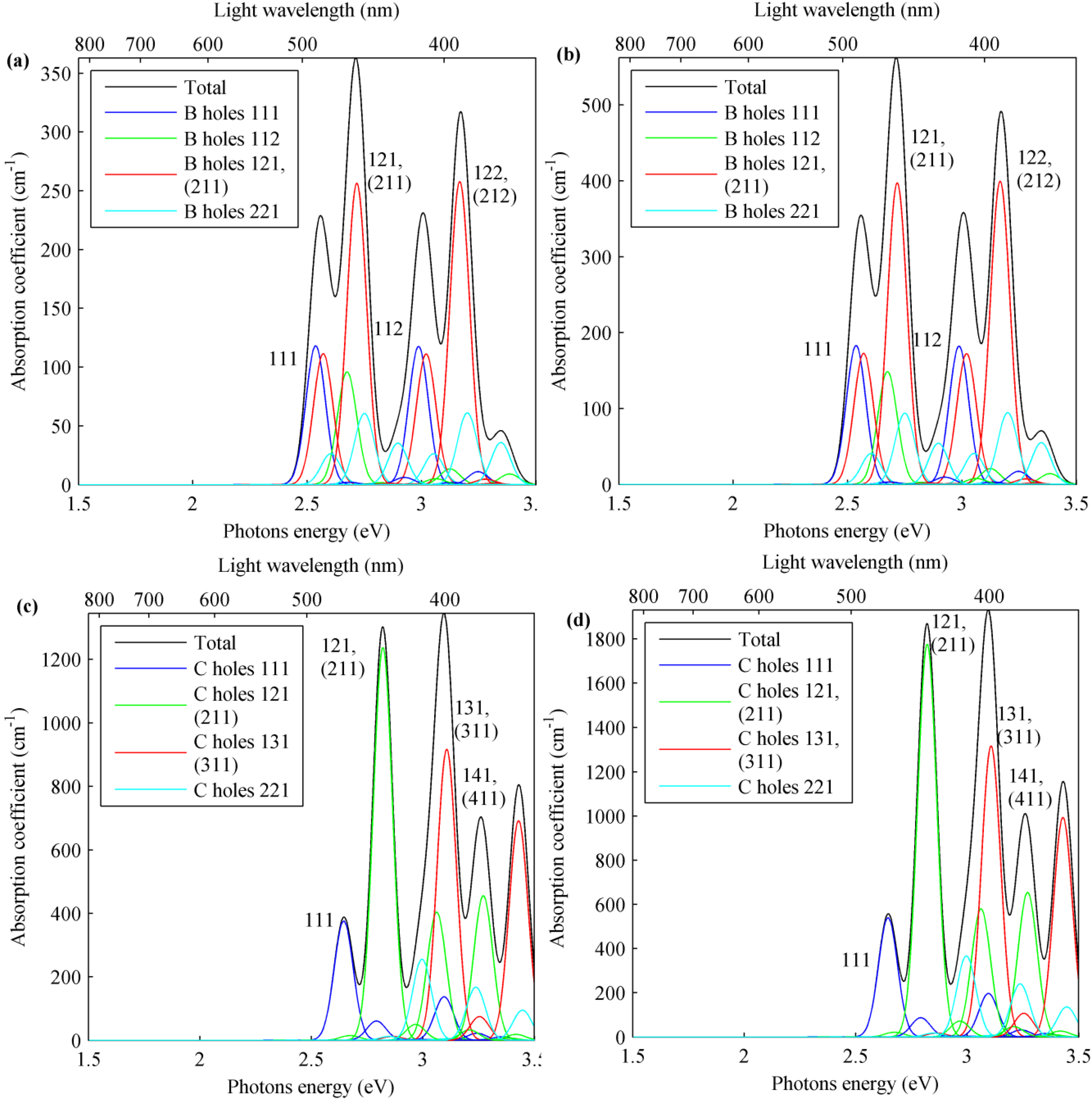
In
Figure 6, the absorption coefficient spectra for interminiband transitions from the B and C valence sub-bands’ to CB for TE- and TM-polarized light are shown. Furthermore, in these cases, absorption profiles are similar for different light polarizations, but absorption values for TM-polarized light are just over one and a half times greater than values for TE-polarized light for transitions involving minibands in the B valence sub-band, while for C, absorption values for TM-polarized light are a little less than one and a half times greater with respect to those for TE-polarized light.
The highest peaks are related to interminiband transitions from the B and C valence sub-band 121 (211) to 121 (211) CB minibands. For transitions from the B valence sub-band, an additional high peak is obtained for interminiband transitions from 121 (211) to 122 (212) in CB (
Table 3).
Table 3.
Interminiband absorption coefficient maximum peaks for In0.4Ga0.6N/GaN QDSL with dot sizes = 4–6 nm, = 3 nm and inter-dot distances = 5 nm and = 2.5 nm evaluated with a Gaussian inhomogeneous linewidth broadening with a full width at half maximum (FWHM) broadening = 100 meV.
Table 3.
Interminiband absorption coefficient maximum peaks for In0.4Ga0.6N/GaN QDSL with dot sizes = 4–6 nm, = 3 nm and inter-dot distances = 5 nm and = 2.5 nm evaluated with a Gaussian inhomogeneous linewidth broadening with a full width at half maximum (FWHM) broadening = 100 meV.
| Interminiband Absorption Coefficient Maximum Peaks | A Holes | B Holes | C Holes |
|---|
| QD Base Lateral Size(nm) |
|---|
| 4 | 5 | 6 | 4 | 5 | 6 | 4 | 5 | 6 |
|---|
| Minibands involved | VB | 111 | 111 | 111 | 111 | 121 | 121 (211) | 121 (211) | 121 (211) | 121 (211) |
| CB | 112 | 112 | 112 | 111 | 111 | 121 (211) | 121 (211) | 121 (211) | 121 (211) |
| Photon energy (eV) (light wavelength (nm)) | 3.16 (392) | 3.06 (405) | 3 (413) | 2.69 (461) | 2.65 (468) | 2.72 (456) | 3.12 (397) | 2.94 (422) | 2.82 (440) |
| Values (cm−1) | TE | 283.5 | 290.6 | 273 | 128.2 | 213.2 | 256.4 | 1164.8 | 1310 | 1236.5 |
| TM | 112.8 | 106.4 | 92.3 | 164.1 | 302.3 | 397.2 | 1778.8 | 1938.5 | 1775.2 |
The behavior of the interminiband absorption coefficient is presented in
Figure 7 for all samples of
Table 2 when QDs’ base sizes are reduced, while keeping the other geometrical and compositional conditions the same.
Figure 6.
Absorption coefficient for interminiband transitions from the B valence sub-band to CB for (a) TE- and (b) TM-polarized light and interminiband transitions from C valence sub-band to CB minibands for (c) TE- and (d) TM-polarized light in In0.4Ga0.6N/GaN QDSL with dot sizes = 6 nm, = 3 nm and inter-dot distances = 5 nm and = 2.5 nm. Integer numbers near the highest peaks specify the CB minibandinvolvedin the absorption process.
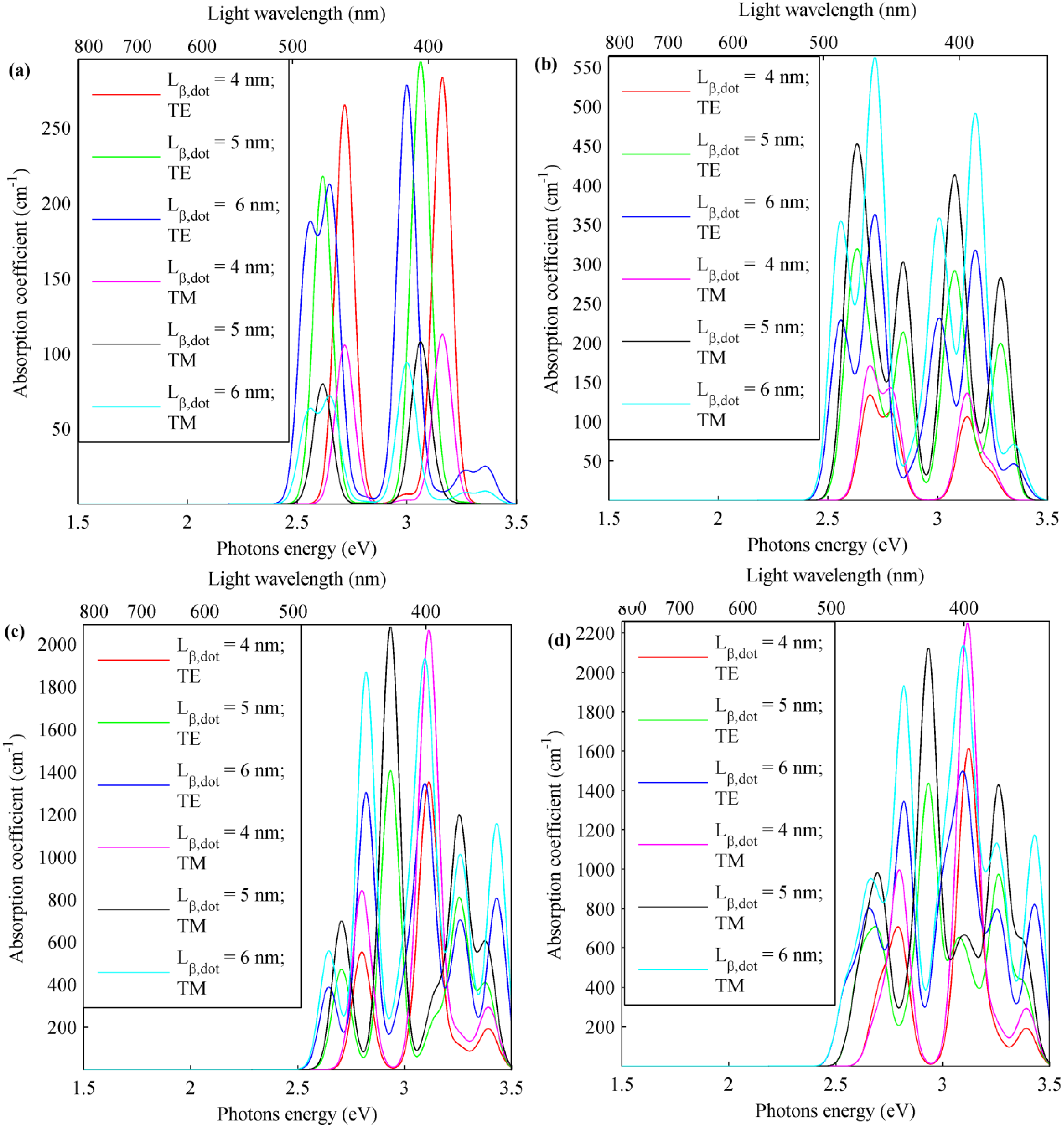
The greater interaction of A valence sub-band minibands with TE-polarized light and of B and C with the TM light polarization described in previous paragraph is confirmed for all samples. Furthermore, for smaller QDs in asuperlattice, a minor number of minibands, corresponding to a thinner bandwidth of the absorption spectrum, is revealed. This is verified for all transitions involving minibands of different valence sub-bands, as is clearly visible in
Figure 7a–c (red and magenta contributions), and consequently, for the total absorption shown in
Figure 7d. On the other hand, the situation is less regular for peaks values of the absorption coefficient. For transitions from the A valence sub-band minibands (a), smaller QDs lead to having higher peaks, while for transitions involving the B valence sub-band minibands (b), the trend is the opposite. In
Figure 7c, a clear tendency is not visible, but this contribution to the total interminiband absorption coefficient (d) is the most significant. However, in total, the interminiband absorption coefficient highest peaks of 2249 and 1613 cm
−1 for TM- and TE-polarized light, respectively, for a photon energy of 3.12 eV (wavelength of 397 nm) are obtained for the smallest QDs. These peaks are derived, above all, by the interminiband transition contributions from A, B and C valence sub-band to 111–112 CB minibands.
Figure 7.
Absorption coefficient for the (a) A, (b) B, (c) C and (d) total valence sub-band CB interminiband transitions for TE- and TM-polarized light in In0.4Ga0.6N/GaN QDSL with variable dot sizes = 4–6 nm, = 3 nm and inter-dot distances = 5 nm and = 2.5 nm.
Figure 7.
Absorption coefficient for the (a) A, (b) B, (c) C and (d) total valence sub-band CB interminiband transitions for TE- and TM-polarized light in In0.4Ga0.6N/GaN QDSL with variable dot sizes = 4–6 nm, = 3 nm and inter-dot distances = 5 nm and = 2.5 nm.
The relatively small values of the absorption coefficient in
Figure 3,
Figure 4 and
Figure 5 is not surprising, since the exciton contribution has been forced to zero. Indeed, in these simulations, our intent is to investigate the influence of the light polarization and the different valence sub-bands on the absorption process.
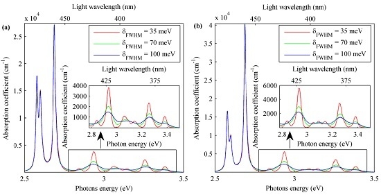
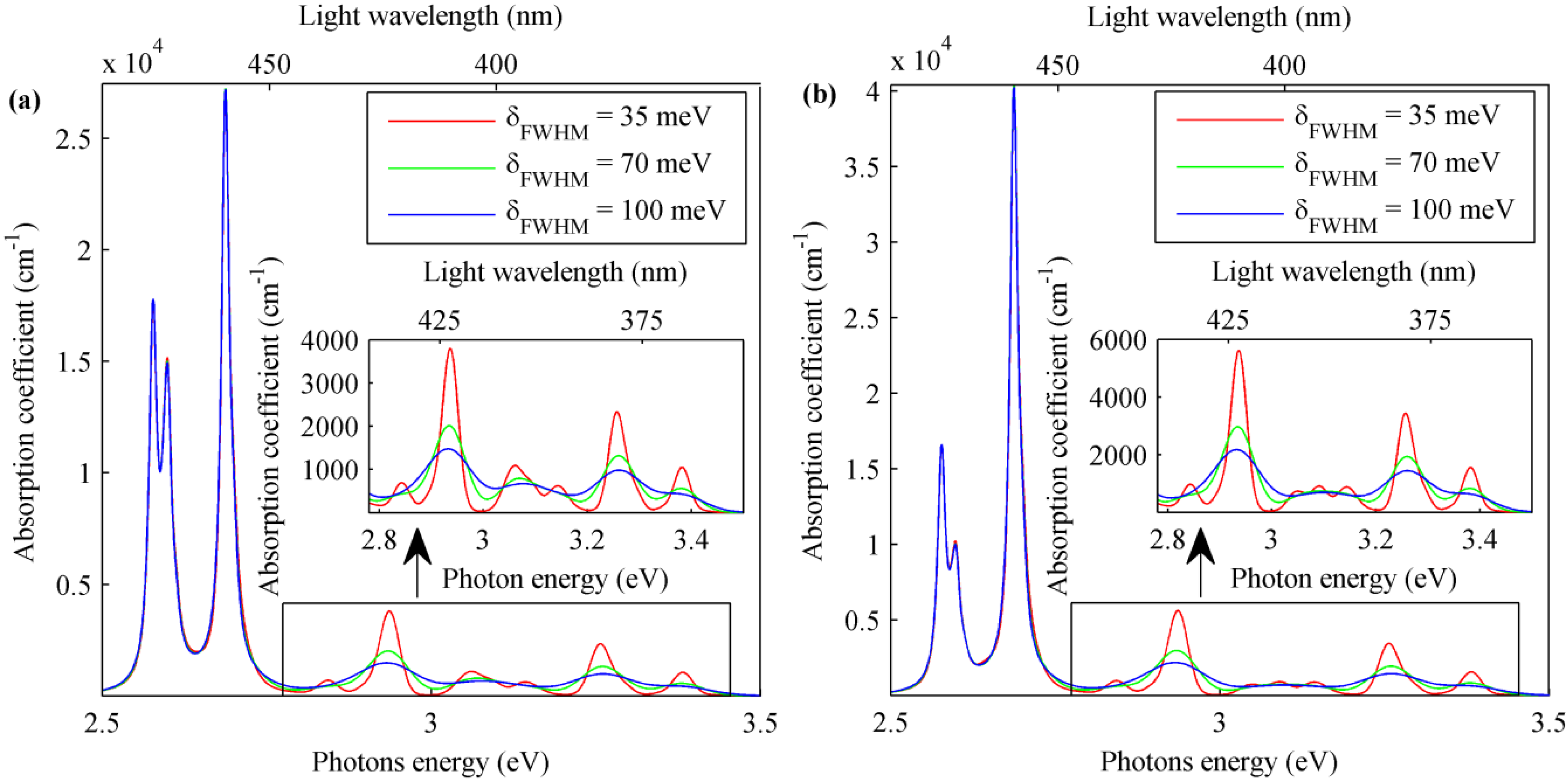
All peak values and spectral widths of the absorption coefficient obtained through our developed model change by varying the spectral broadening for each transition introduced through a Gaussian inhomogeneous linewidth broadening (
) (Equation (C2) in
Appendix C). For the samples shown, a
= 100 meV constant for each photon energy has been used. This model fitting parameter could be chosen with appropriate values variable with the photon energy in order to allow a better matching between the absorption coefficient predicted by the model and empirical measures. Indeed, linewidth broadening depends on geometrical (size of dots and regularity of their distribution) and compositional fluctuation (spatial variation of In content in the structure) that can influence in a different manner the absorption coefficient for various photon energies. The
influence on the absorption coefficients is given in
Figure 8, in which the exciton effect is also introduced for the second structure shown in
Table 2. A broadening of
= 7 meV for the exciton absorption is assumed as a good trade-off between very high exciton absorption coefficient peaks and its spectral width withrespect to that of the interminiband absorption obtained by the model. Furthermore, in this case, the value of broadening
is a fitting parameter of the model for a more accurate matching with the actual empirical measures of the exciton absorption coefficient for the structure.
In
Figure 8, the first highest three peaks visible on the blue curve for both TE- (a) and TM-polarized light (b) from left to right are related to the exciton effect for the B, A and C valence sub-band CB interminiband transitions, respectively. Even for exciton peaks, transitions involving minibands in the A valence sub-band are characterized by a greater interaction with TE light polarization, while for minibands in the C valence sub-band, the opposite situation occurs. As is visible in
Figure 8, the exciton absorption coefficient peaks for transitions from the A and B valence sub-bands minibands are obtained for very near photon energy values (2.6 and 2.58 eV, corresponding to wavelengths of 477 and 480 nm, respectively, for the transition involving the first miniband in the A and B valence sub-bands). Then, both peak values are influenced by the other and, in this case, are higher for TE light polarization. When QDs’ In concentration x changes in an In
xGa
1-xN/GaN QDSL, all of their electronic and optical properties are modified. For example, the barrier potentials for charge carriers in QDs can be increased or decreased according to the QD In
xGa
1-xN band gap variation with respect to the GaN of barrier regions. In
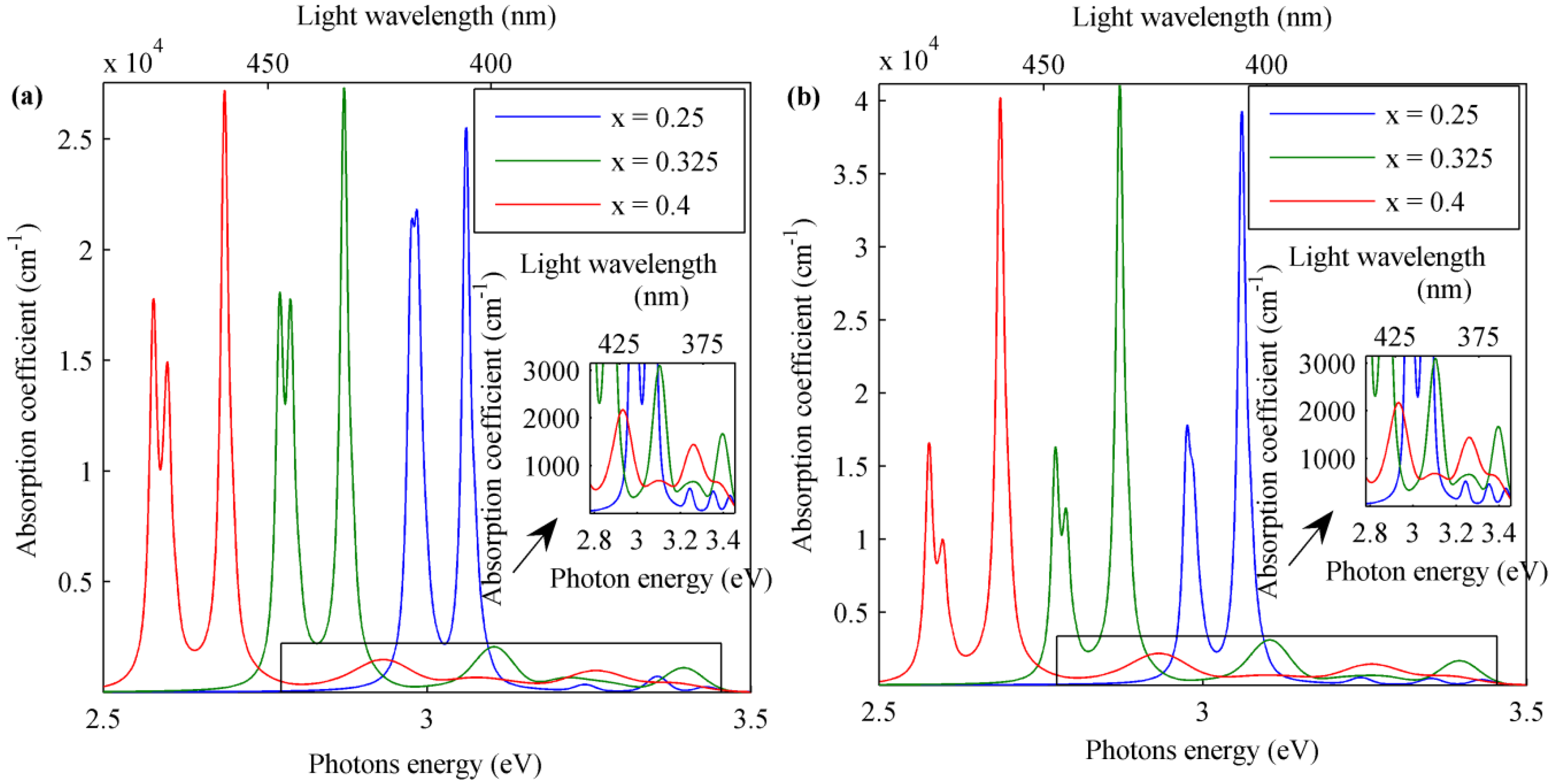
Figure 9, interminiband absorption coefficients are shown for different QDSL samples with the same geometrical structure, but different QDs’ In content
x = 0.25, 0.325 and 0.4. Excitonic parameters are reported in
Table 4.
Figure 8.
Total interminiband transition absorption coefficient with theexcitonic effect for (a) TE- and (b) TM-polarized light in In0.4Ga0.6N/GaN QDSL with dot sizes = 5 nm, = 3 nm and inter-dot distances = 5 nm and = 2.5 nm evaluated with a spectral broadening of = 7 meV and = 35–100 meV for the excitonic and interminibands’ absorption contributions, respectively.
In the structure with a greater
x value, the band gap in QDs is lower, and the absorption spectrum is characterized by a red shift with respect to the samples with smaller
x. For this reason, in
Figure 9, the absorption spectrum of In
0.4Ga
0.6N/GaN QDSL (red line) extends starting from a photon energy of about 2.5 eV (a wavelength of about 500 nm) with respect to the structure with a lower
x value (green and blue line) with a spectrum from about 2.7 and 2.8 eV. Further, the QDSL miniband number for
x = 0.4 is greater than in other samples, so increasing its spectrum extension. In order to have absorption for greater wavelengths (lower photon energy), it is possible to increase the In concentration in the structure. Absorption coefficients for an In
xGa
1-xN/In
0.45Ga
0.55N QDSL for different
x values are shown in
Figure 10. Then, with
x = 1 (InN/In
0.45Ga
0.55N QDSL),the absorption for a wavelength until about 1000 nm (around 1.2 eV) can be achieved with a spectrum until about 1.8 eV for interminiband transitions. This additional absorption contribution due to the miniband formation in superlattices increases the total absorption of an InN/In
0.45Ga
0.55N QDSL given by the other contribution related to interband transition into the barrier for high photon energy over 1.9 eV (about In
0.45Ga
0.55N band gap). Thus, this total absorption spectrum of an InN/In
0.45Ga
0.55N QDSL corresponds to that of an ideal intermediate band solar cell (IBSC) with one intermediate band and optimal band gaps values of 0.71, 1.24 and 1.95 eV for a maximum theoretical efficiency of this structure as presented in different works [
53,
54].
Table 4.
Exciton parameters for InxGa1-xN/GaN QDSL with dot sizes = 5 nm, = 3 nm, inter-dot distances = 5 nm, = 2.5 nm, In content x = 0.25–0.4 and a spectral broadening = 7 meV.
Table 4.
Exciton parameters for InxGa1-xN/GaN QDSL with dot sizes = 5 nm, = 3 nm, inter-dot distances = 5 nm, = 2.5 nm, In content x = 0.25–0.4 and a spectral broadening = 7 meV.
| Excitonic Parameters | A Holes | B Holes | C Holes |
|---|
| In Content (x) |
|---|
| 0.25 | 0.325 | 0.4 | 0.25 | 0.325 | 0.4 | 0.25 | 0.325 | 0.4 |
|---|
| (meV) | 18.23 | 17.65 | 17.09 | 20.07 | 20.43 | 20.03 | 17.64 | 17.4 | 17.09 |
| (nm) | 3.98 | 4.09 | 4.21 | 3.5 | 3.53 | 3.59 | 4.11 | 4.15 | 4.21 |
| Peak values (cm−1) | TE | 14,588 | 12,958 | 11,753 | 15,596 | 15,690 | 16,225 | 24,681 | 26,368 | 26,323 |
| TM | 8422 | 7493 | 6806 | 14,324 | 14,713 | 15,456 | 38,191 | 39,852 | 39,119 |
Figure 9.
Total interminiband transition absorption coefficient with superlattice excitonic effect for (a) TE- and (b) TM-polarized light in InxGa1-xN/GaN QDSL with dot sizes = 5 nm, = 3 nm inter-dot distances = 5 nm, = 2.5 nm and QD In content x = 0.25–0.4.
Figure 9.
Total interminiband transition absorption coefficient with superlattice excitonic effect for (a) TE- and (b) TM-polarized light in InxGa1-xN/GaN QDSL with dot sizes = 5 nm, = 3 nm inter-dot distances = 5 nm, = 2.5 nm and QD In content x = 0.25–0.4.
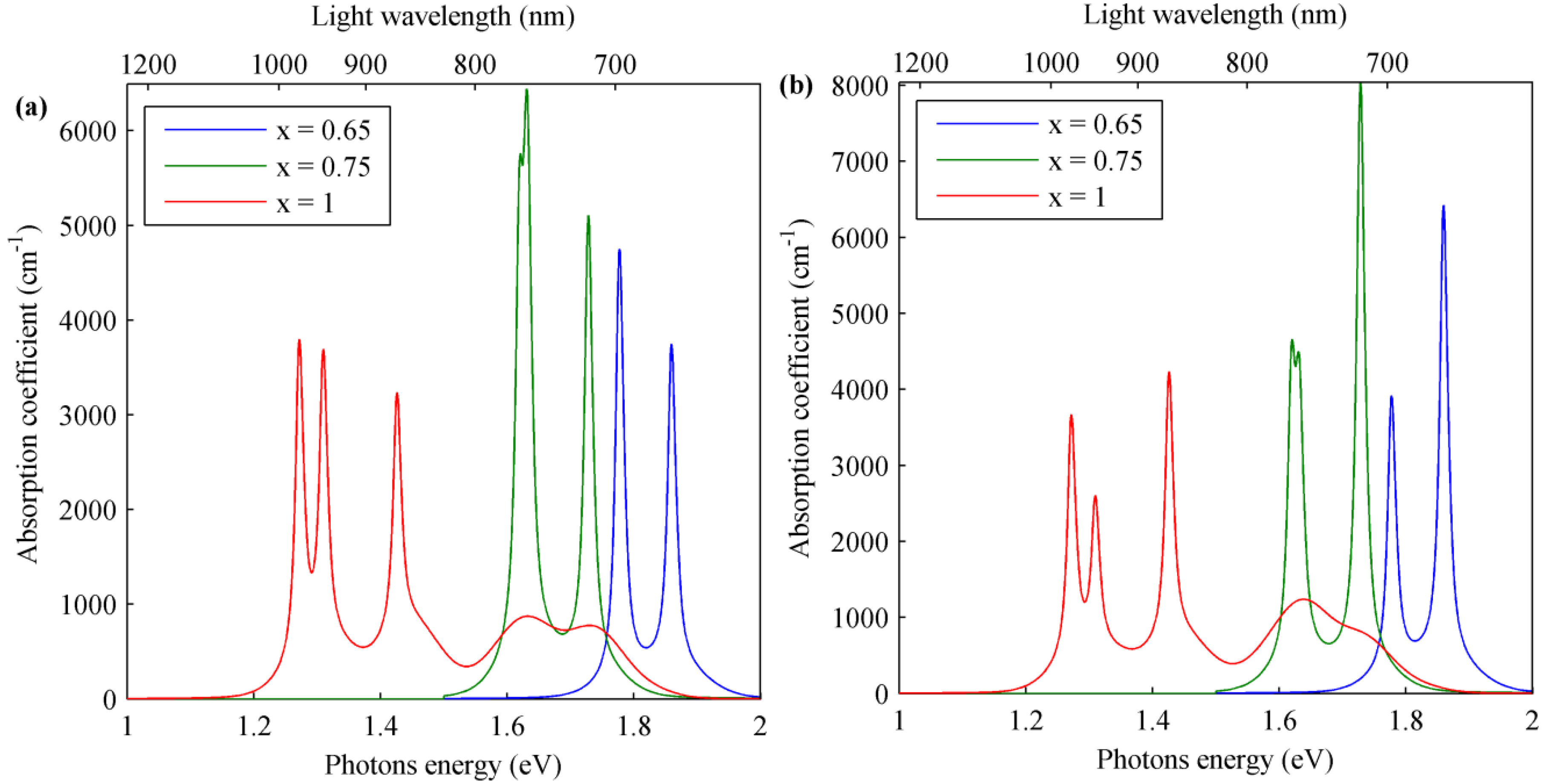
For lower
x values (green and blue lines in
Figure 10), charge carriers’ barrier potential is lower and allows the formation of a smaller number of minibands with a spectrum around that of the exciton effect. Finally,
Figure 6,
Figure 7 and
Figure 8 reveal that the exciton effect increases the absorption coefficient of the order of 10
4 cm
−1 depending on the light polarization and QD In content. Moreover, higher absorption values occur for TM light polarization.
Thus, generally speaking, an increasing of the QD In content induces two main effects. The former is the energy bandgap reduction, resulting in the red shift absorption. The latter is the change of the piezoelectric effect as induced by an increased lattice mismatch between dot and barrier materials.
Figure 10.
Total interminiband transition absorption coefficient with the superlattice excitonic effect for (a) TE- and (b) TM-polarized light in InxGa1-xN/In0.45Ga0.55N QDSL with dot sizes = 5 nm, = 3 nm, inter-dot distances = 5 nm, = 2.5 nm and QDs In content x = 0.65–1.
Figure 10.
Total interminiband transition absorption coefficient with the superlattice excitonic effect for (a) TE- and (b) TM-polarized light in InxGa1-xN/In0.45Ga0.55N QDSL with dot sizes = 5 nm, = 3 nm, inter-dot distances = 5 nm, = 2.5 nm and QDs In content x = 0.65–1.


