Abstract
This paper reports a hybrid integrated light source fabricated on a silicon platform using a 1.3 μm wavelength quantum dot array laser. Temperature insensitive characteristics up to 120 °C were achieved by the optimum quantum dot structure and laser structure. Light output power was obtained that was high enough to achieve an optical error-free link of a silicon optical interposer. Furthermore, we investigated a novel spot size convertor in a silicon waveguide suitable for a quantum dot laser for lower energy cost operation of the optical interposer.
1. Introduction
Optical interconnect technology taking advantage of the high speed of light is expected to solve electrical band width bottleneck as demand increases for Tb/s-class high speed interconnects [1]. We previously proposed a photonics-electronics convergence system to solve the bandwidth bottleneck problem among large scale integrations (LSIs) and demonstrated silicon optical interposers fully integrated with optical components on a silicon substrate, achieving a high bandwidth density of 30 Tbps/cm2 at room temperature [2]. Here, the light source was a hybrid integrated by a flip-chip mounting technique using passive alignment. We think that the hybrid integrated light source is suitable for a high density silicon optical interposer from the viewpoint of large output power and low energy cost operation.
On the other hand, a light source on a silicon optical interposer mounted on LSI chips consumes more power as the temperature is increased by the heat generated in the LSIs (up to about 85 °C or higher) [3]. Because a laser diode (LD) serving as a light source is particularly sensitive to the effects of a temperature increase, we examined a temperature-insensitive hybrid integrated light source on a Si platform to apply a quantum dot (QD) LD with high-temperature characteristics [4]. Furthermore, to increase bandwidth density, we applied a small array LD as an optical interposer light source [5]. Also, small QD array LDs should be mounted on light sources for an optical interposer.
In this paper, we discuss the 1.3 μm QD array LD, particularly parts that have not been described in detail so far, and report characteristics of an integrated light source on a silicon substrate. We also discuss lower energy cost operation of a silicon optical interposer by using an improved spot size convertor suitable for a QD LD spot size.
2. 1.3-μm Wavelength Quantum Dot Lasers
Self-assembled InAs quantum dots that emit at 1.3-μm wavelength are structures of several tens of nanometers grown on a GaAs substrate in the Stranski-Krastanow mode. QDs are expected to improve lasing characteristics, such as low threshold current operation, high speed direct modulation and low noise due to small linewidth enhancement factor, more than bulk or quantum-well (QW) devices, resulting from three-dimensional carrier confinement [6]. Moreover, it was reported that p-type doping in QDs enabled highly temperature-stable LD performance in a wide temperature range [7,8].
For a QD LD as a light source, highly efficient coupling into silicon waveguide is as important as high power operation at high temperature. We aimed at over 2 mW operation into a silicon waveguide from 25 °C to 85 °C in order to achieve high bandwidth density in the temperature range [9]. The stack number of QD layers should be large and optical mode field should be strongly confined in the active region from the viewpoint of increasing optical gain for high power operation at high temperature. However, strong confinement leads to large coupling loss between a QD LD and a silicon waveguide, so the optical field needs to expand out the QD active layer to some extent for highly efficient coupling. We set the stack number of the QD layers to eight in order to both increase optical gain and achieve high efficiency coupling. Dot density in plane, which is a quite important factor to enlarge optical gain as well as stacking number, was set to 6×1010 cm–2.
Figure 1 shows a schematic structure of a QD array LD fabricated at QD Laser, Inc. The LD structure was grown on a GaAs substrate by molecular beam epitaxy (MBE). The QD uniformity was improved by suppressing indium out-diffusion during QD coverage growth, resulting in enhanced optical gain [10]. The QD active layers were sandwiched between the AlGaAs lower cladding layer and the InGaP upper-cladding layer. The active layers were eight stacked QD layers partially p-type doped. An array LD structure with multiple QD active region stripes was fabricated. Each waveguide was a ridge waveguide structure with the mesa-width of 1.7 μm and the cavity length of 600 μm. Current was injected into each active region through a single electrode on the top surface, and all the stripes emitted laser light output simultaneously. Highly reflective coatings of 30% and 90% were placed on the front and the rear facets, respectively. Figure 1b shows light-current characteristics of a QD array LD where 13 curves from each active stripe were overwritten. Measurements were demonstrated at 25 °C, and the light outputs were measured by using a lensed fiber for each channel. The threshold currents were about 5.4 mA in all stripes, and the uniform 13 light outputs were obtained within 0.1 dB power fluctuation.
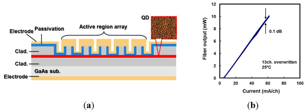
Figure 1.
Structure and characteristics of a QD array LD: (a) Schematic structure. (b) Light-current characteristics. Thirteen curves were overwritten.
Figure 2 shows the array number dependence of threshold currents and slope efficiencies of the QD array LDs and the top-view photographs of one-, seven-, and 13-channel arrays. The slope efficiency was calculated by using all injection current and all the light output detected by a large diameter detector. The threshold currents were proportional to the array number, and the efficiency did not depend on the array number. This means that the variations in the production of each channel were small and that the current was injected into each stripe equally. No LD characteristic degradations caused by the array structure were observed.
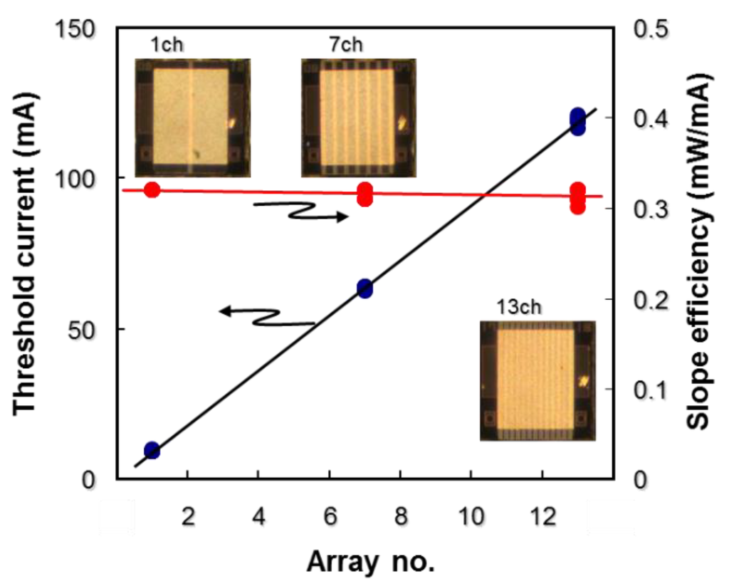
Figure 2.
Threshold current and slope efficiency of QD array LDs.
P-type doping into the QD active region improves temperature characteristics of the QD LD. However, the excess doping causes internal loss to increase, quantum efficiency to degrade, and LD characteristics to deteriorate: threshold current increases and slope efficiency decreases [11]. Appropriate p-type doping concentration needs to be investigated. We evaluated temperature dependence of light output characteristics of a 13-channel array LD mounted on an AlN heatsink. The p-type doping concentration in the QD active region was 5 × 1017 cm–3. This doping level is converted to six acceptors per QD by taking into account of the QD sheet density and the QD height of 7 nm [10]. All output power from each channel was detected simultaneously by a large diameter detector. Figure 3a shows light output characteristics from 25 °C to 120 °C. Over 10 mW output power was obtained at 100 °C. Figure 3b shows the doping concentration dependence of the LD light power degradation from the light power at 25 °C and 20 mW. The degradation of the 5 × 1017 cm–3 doped LD exhibited smaller dependence than that of the 2 × 1017 cm–3 doped LD. We think that the p-type doping concentration of 5 × 1017 cm–3 is desirable in the application for our optical interposer light source, taking into account the possibility of LD characteristics degrading due to a higher doping concentration.
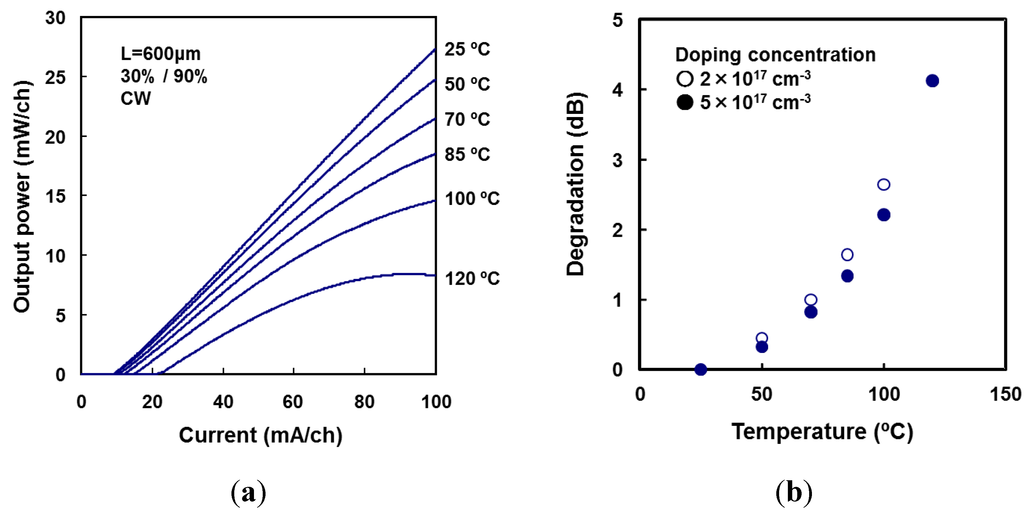
Figure 3.
Light output characteristics. (a) Temperature dependence. (b) p-type doping concentration dependence.
3. A Quantum Dot Light Source Mounted on a Silicon Platform
3.1. Fabrication and Evaluation
We fabricated a hybrid integrated light source with Si waveguides—including trident spot size convertors (SSCs) [9], a LD mounting stage with pedestals, and germanium (Ge) photo detectors on a silicon on insulator (SOI) substrate of 200-nm-thick Si core—and mounted the QD LD by passive alignment flip-chip bonding. The QD LD had 13-channel arrayed stripes with a 30 μm pitch. Current was injected into each active region through a single electrode. Figure 4a schematically shows the light source structure.
Figure 4b shows the characteristics of the light power coupled into the Si waveguide as a function of injection current, with the measurement temperature ranging from 25 °C to 120 °C. The threshold current was 11 mA at 25 °C and 30 mA at 120 °C. The light output power was measured by a Ge photo detector integrated on the same Si wafer. The light output temperature dependence was likewise insensitive in the same way as the light output characteristic of the QD LD mounted on an AlN heat sink shown in Figure 3a. Power degradation was minimal from 25 °C on up, staying within about 0.6 dB up to 85 °C and within about 2.5 dB up to 100 °C. From these measurements, we found that coupled light output into a Si waveguide of more than 2 mW was obtained up to 120 °C. This means that an optical link can be demonstrated at temperatures up to 120 °C taking into account the loss budget [2]. We also experimentally demonstrated error free operation up to 125 °C [4].
We also evaluated the light output uniformity of nine channels, because the Ge photo detectors were not installed in the other four. The light output characteristics in Figure 4b were obtained from the channel 7. The characteristics were typical results of the array light source. As shown in Figure 4c, the output power variation of the nine channels was less than 1.3 dB, although this uniformity included the variation in coupling loss, waveguide loss, and LD output power. Misalignment loss due to channel position was also included. In order to achieve all channel error free operation in a silicon optical interposer, there is possibility that the injection current into the LD should be increased to compensate the power variation.
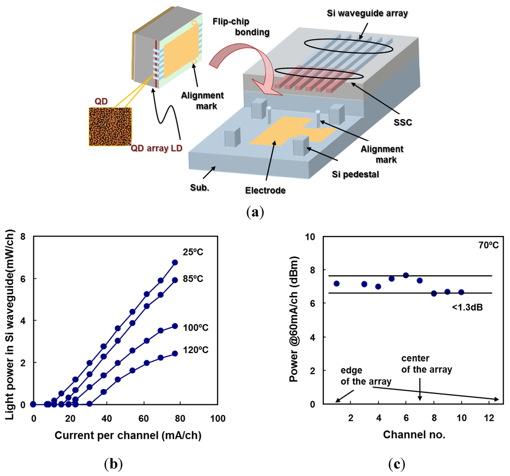
Figure 4.
A hybrid integrated light source. (a) Schematic structure. (b) Light output characteristics. (c) Output power uniformity from each channel.
3.2. A Novel Spot Size Convertor for Highly Efficient Coupling between a QD LD and a Silicon Waveguide
Improving coupling efficiency between a silicon waveguide and an external light source is an important issue [12,13]. We applied a trident SSC for coupling between a QD LD and a silicon waveguide. Because a QD LD is characterized as having strong optical confinement in the vertical direction, the spot size is a quite flat elliptical shape. Therefore, the coupling tolerance is smaller in the vertical direction than in the horizontal direction. Coupling loss can be improved by forming a SSC spot size the same size as the QD LD, but the alignment accuracy requirement becomes strict because of low misalignment tolerance. Thus, we have investigated a novel triple-core SSC (as shown in Figure 5) to achieve both low coupling loss and high misalignment tolerance simultaneously. We designed the side waveguides to spread more widely than a trident SSC in order to expand the horizontal optical mode. Moreover, a center waveguide is extended to the facet to suppress multi-mode excitation. From simulations, the minimum coupling loss without misalignment was estimated to be 2.5 dB between the triple-core SSC (200 nm Si core thickness, 2 μm separated side waveguides, and 130 nm tip width) and a QD LD (4 μm and 1 μm spot-size for horizontal and vertical directions). Improvement of more than 1 dB above the coupling loss of a trident SSC can be expected.
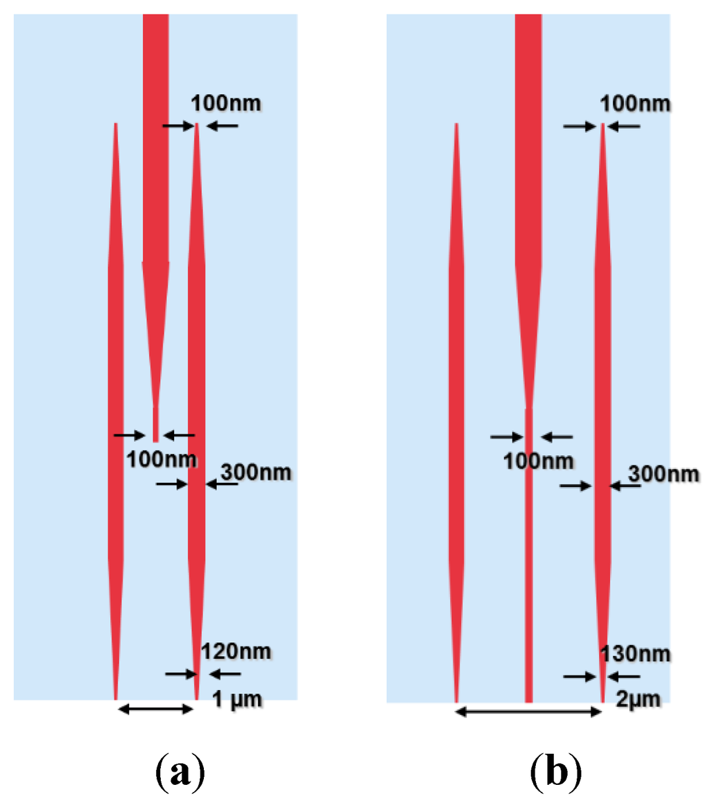
Figure 5.
Spot size convertor structures for a 1.3 μm wavelength QD LD. (a) Trident spot size convertors (SSC). (b) Triple-core SSC.
We fabricated a triple-core SSC on an SOI substrate of 200-nm-thick Si core and evaluated coupling loss between the SSC and a 1.3 μm QD LD by active alignment. The triple-core SSC facet was formed by polishing. The QD LD had a single active region stripe. Optical power was measured at the other end facet during moving the LD in the horizontal or vertical direction and injecting current into the LD. The minimum loss at zero deviation of 3.0 dB was obtained from two SSC-sample active alignment measurements, and 1 dB improvement above that using a conventional trident SSC was demonstrated. Figure 6 shows the optical coupling tolerance measured by moving the QD LD horizontally or vertically. The tolerance up to a 1 dB loss increase was ± 0.61 μm in the horizontal direction and ± 0.45 μm in the vertical direction. Because the accuracy obtained in flip-chip mounting an LD can be controlled to less than ± 0.5 μm in the horizontal direction by using a precise alignment technique and less than ± 0.1 μm in the vertical direction by etch-depth control in forming the Si pedestals, the maximum coupling loss can be suppressed to less than the minimum coupling loss about 1 dB.
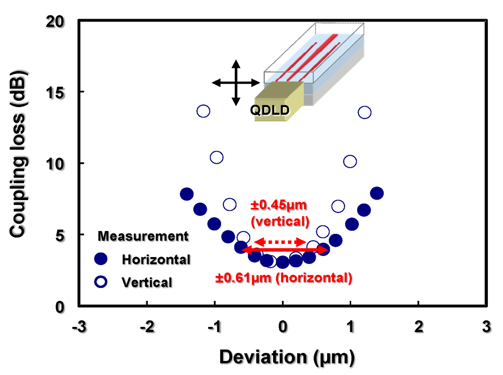
Figure 6.
Coupling characteristics of a triple-core SSC for 1.3 μm wavelength and a QD LD. Minimum coupling loss was about 3.0 dB at zero deviation.
We discussed how coupling loss reduction affects low energy cost operation of an optical interposer. We reported low power consumption and low energy cost operation of light sources of optical interposers that employed optical splitters [14,15]. Here, we discuss energy cost of a QD LD when an optical splitter divides the light output into two waveguides. Figure 7 shows the calculation results of energy cost of the light source against SSC loss using parameters of the fabricated optical interposer, which included wall-plug efficiency of a QD LD, SSC coupling loss, waveguide loss, modulator loss, splitter loss, photo detector sensitivity, and other excess loss. Figure 7 also shows the result obtained by Urino et al.: 2.9 pJ/bit [4]. We demonstrated 12.5 Gbps data transmission in each two-branched channel with a minimum received power of -7 dBm. Here, the 13-channel QD array LD consumed 957 mW, which corresponds to 36.8 mW/channel, because the capacity of the array LD was 26 output channels. Taking into account the 12.5 Gbps signal transmission, an energy cost of 2.9 pJ/bit was obtained. The deviations of the experimental results from simulations are attributed to additional excess losses. Low energy cost operation below 1 pJ/bit [16] is expected by 3 dB coupling loss using the triple-core SSC along with decreasing waveguide loss or modulator loss and operation speed increasing as high as 25 Gbit/s. This triple-core SSC is promising for application to a hybrid integrated light source using a QD LD for optical interconnects.
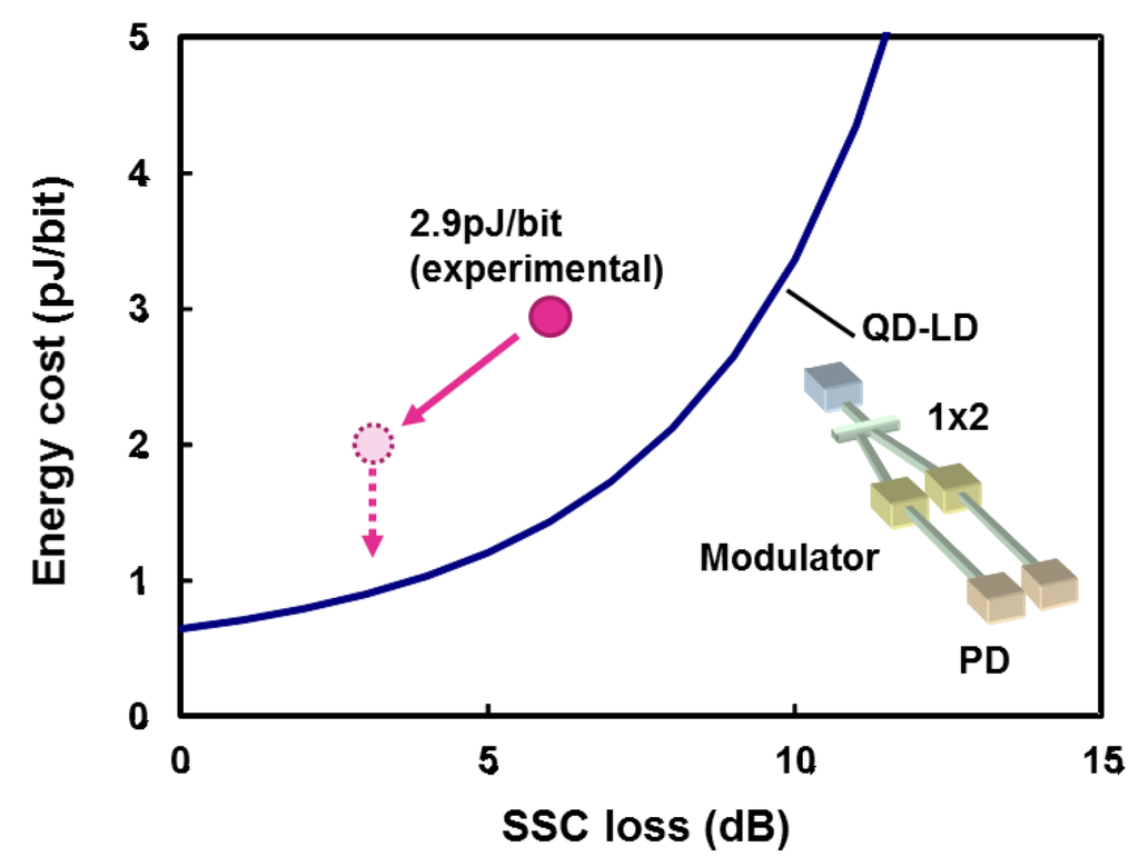
Figure 7.
Energy cost estimation of a QD LD as a light source of a silicon optical interposer and experimental results. Low energy cost operation below 1 pJ/bit is expected using the triple-core SSC along with decreasing excess losses and high speed operation.
4. Conclusions
We demonstrated a QD LD as a light source for a silicon optical interposer from the viewpoint of insensitive temperature dependence and high optical coupling into a silicon waveguide. We optimized the QD stack number, doping concentration, and LD cavity structure for our purpose and realized a QD array LD with high light output operation up to 120 °C. We also fabricated a hybrid integrated light source on a Si platform using the QD array LD operating at 1.3 μm wavelength, and this light source is suitable for applications with an operating temperature around 120 °C. We investigated the low energy cost operation of light sources for large-scale inter-chip optical interconnects. The QD LD is promising for application to the integrated light source of optical interconnects when temperature-insensitive characteristics are required.
Acknowledgments
The authors thank Masashige Ishizaka for his fruitful discussions. This research is supported by the Japan Society for the Promotion of Science (JSPS) through its “Funding Program for World-Leading Innovative R&D on Science and Technology (FIRST Program)” and by the New Energy and Industrial Technology Development Organization (NEDO). The authors also thank the TIA-SCR Management Office, AIST, for their technical support and device fabrication.
Author Contributions
Nobuaki Hatori, Takanori Shimizu and Makoto Okano performed the theoretical calculations, device design, device fabrication and experiments. Nobuaki Hatori, Yutaka Urino, Takanori Shimizu, Makoto Okano, Yutaka Urino, Tsuyoshi Yamamoto, Masahiko Mori, Takahiro Nakamura and Yasuhiko Arakawa discussed the results and co-wrote the manuscript. Yasuhiko Arakawa supervised the research.
Conflict of Interest
The authors declare no conflicts of interest.
References
- Young, I.A.; Mohammed, E.M.; Liao, J.T.S.; Palermo, A.M.; Block, B.A.; Reshotko, M.R.; Chang, P.L.D. Optical technology for energy efficient I/O in high performance computing. IEEE Commun. Mag. 2010, 10, 184–191. [Google Scholar] [CrossRef]
- Urino, U.; Usuki, T.; Fujikata, J.; Ishizaka, M.; Yamada, K.; Horikawa, T.; Nakamura, T.; Arakawa, Y. High-density and wide-bandwidth optical interconnects with silicon optical interposers. Photon. Res. 2014, 3, A1–A7. [Google Scholar] [CrossRef]
- Assembly and Packaging, Table AP2, International Technology Roadmap for Semiconductors, 2012. Available online: http://www.itrs.net/ITRS 1999-2014 Mtgs, Presentations & Links/2012ITRS/Home2012.htm, Assembly & Packaging 2012 tables (accessed on 30 March 2015).
- Urino, U.; Hatori, N.; Akagawa, T.; Shimizu, T.; Okano, M.; Ishizaka, M.; Yamamoto, T.; Okayama, H.; Onawa, Y.; Takahashi, H.; et al. First Demonstration of Athermal Silicon Optical Interposers with Quantum Dot Lasers Operating up to 125 °C. In Proceedings of European Conference on Optical Communications, Cannes, France, 21–25 September 2014.
- Shimizu, T.; Hatori, N.; Okano, M.; Ishizaka, M.; Yamamoto, T.; Urino, Y.; Mori, M.; Nakamura, T.; Arakawa, Y. High density hybrid integrated light source with a laser diode array on a silicon optical waveguide platform for inter-chip optical interconnection. In Proceedings of IEEE International Conference on Group IV Photonics, London, UK, 14–16 September 2011.
- Arakawa, Y.; Sakaki, H. Multidimensional quantum well laser and temperature dependence of its threshold current. Appl. Phys. Lett. 1982, 40, 939–941. [Google Scholar] [CrossRef]
- Otsubo, K.; Hatori, N.; Ishida, M.; Okumura, S.; Akiyama, T.; Nakata, Y.; Ebe, H.; Sugawara, M.; Arakawa, Y. Temperature-Insensitive Eye-Opening under 10-Gb/s Modulation of 1.3-μm P-Doped Quantum-Dot Lasers without Current Adjustments. Japan. J. Appl. Phys. 2004, 8B, L1124–L1126. [Google Scholar]
- Tanaka, Y.; Ishida, M.; Takada, K.; Yamamoto, T.; Song, H.; Nakata, Y.; Yamaguchi, M.; Nishi, K.; Sugawara, M.; Arakawa, Y. 25 Gbps direct modulation in 1.3-μm InAs/GaAs high-density quantum dot lasers. In Proceedings of Conference on Lasers and Electro-Optics, San Jose, CA, USA, 16–21 May 2010.
- Hatori, N.; Shimizu, T.; Okano, M.; Ishizaka, M.; Yamamoto, T.; Urino, Y.; Mori, M.; Nakamura, T.; Arakawa, Y. A Hybrid Integrated Light Source on a Silicon Platform Using a Trident Spot-Size Converter. J. Lightw. Technol. 2014, 7, 1329–1336. [Google Scholar] [CrossRef]
- Nishi, K.; Kageyama, T.; Yamaguchi, M.; Maeda, Y.; Takemasa, K.; Yamamoto, T.; Sugawara, M.; Arakawa, Y. Molecular beam epitaxial growths of high-optical-gain InAs quantum dots on GaAs for long-wavelength emission. J. Cryst. Growth 2013, 378, 459–462. [Google Scholar] [CrossRef]
- Shchekin, O.B.; Deppe, D.G. 1.3 μm InAs quantum dot laser with T0 = 161 K from 0 to 80 °C. Appl. Phys. Lett. 2002, 18, 3277–3279. [Google Scholar] [CrossRef]
- Tao, S.H.; Song, J.; Fang, Q.; Yu, M.B.; Lo, G.Q.; Kwong, D.L. Improving coupling efficiency of fiber-waveguide coupling with a double-tip coupler. Opt. Express 2008, 16, 20803–20808. [Google Scholar] [CrossRef] [PubMed]
- Romero-García, S.; Marzban, B.; Florian, M.; Shen, B.; Witzens, J. Edge Couplers with Relaxed Alignment Tolerance for Pick-and-Place Hybrid Integration of III–V Lasers with SOI Waveguides. J. Select. Top. Quant. Electron. 2014, 20, 369–379. [Google Scholar] [CrossRef]
- Hatori, N.; Shimizu, T.; Okano, M.; Ishizaka, M.; Yamamoto, T.; Urino, Y.; Mori, M.; Nakamura, T.; Arakawa, Y. 2.2 pJ/bit Operation of Hybrid Integrated Light Source on A Silicon Optical Interposer for Optical Interconnection. In Proceedings of IEEE Photonics Conference, Seattle, WA, USA, 8–12 September 2013.
- Hatori, N.; Shimizu, T.; Okano, M.; Ishizaka, M.; Yamamoto, T.; Urino, Y.; Mori, M.; Nakamura, T.; Arakawa, Y. Low Power Consumption Operation of Light Sources for Inter-chip Optical Interconnects. In Proceedings of International Conference on Indium Phosphide and Related Materials, Kobe, Japan, 19–23 May 2013.
- Zheng, X.; Lin, S.; Luo, Y.; Yao, J.; Li, G.; Djordjevic, S.S.; Lee, J.H.; Thacker, H.D.; Shubin, I.; Raj, K.; et al. Efficient WDM Laser Sources towards Terabyte/s Silicon Photonic Interconnects. J. Lightw. Technol. 2013, 24, 4142–4154. [Google Scholar]
© 2015 by the authors; licensee MDPI, Basel, Switzerland. This article is an open access article distributed under the terms and conditions of the Creative Commons Attribution license (http://creativecommons.org/licenses/by/4.0/).